1. Introduction
The distributed generator using renewable energy is currently regarded as the premium supplement form for conventional fossil energy [
1]. Unlike the conventional grid, the distributed generation system is vulnerable to disturbances. Whether the distributed generation system is in grid-connected mode or islanded mode, an undamped disturbance may greatly affect the connected apparatuses. Considering the demand of the local load, multifunctional inverters are applied in these systems [
2]. Inverters are currently expected to participate in grid-forming, harmonic compensation, microgrid voltage supported, all of which improve the system’s stability and promote its performance [
3,
4,
5].
For this paper, the inverter operating in islanded mode was investigated. The harmonic current and the harmonic voltage issues can be serious when they appear in islanded mode, unlike in the grid-connected mode. The harmonic current will lead to voltage sag in the system. The harmonic voltage will increase the system’s power loss, reduce the power factor, and even disconnect the voltage sensitive apparatuses from the microgrid [
6]. Moreover, considering that the system power transfer relies on the paralleled converters connecting to the AC bus, harmonic voltage may lead to a circulating current issue. To cope with this issue, the isolated transformers, which will form the impedance to the circulating current, are applied in inverters [
7]. However, isolated transformers make the apparatus bulky and costly. Furthermore, the line impedance cannot mitigate the low-order harmonic elements. Therefore, in order to improve system performance, several strategies aiming to decrease the harmonic voltage are proposed by scholars [
8,
9,
10].
The virtual capacitor is utilized to compensate the harmonic components existing in the voltage [
11,
12]. However, virtual capacitors may form resonant circuits with the output inductor, which is hardly damped [
13,
14]. To compensate that resonance, virtual resistors are needed, whose presence introduces voltage sag into the system. Moreover, when several resonant controllers exist in a paralleled system, the impedance and the resonant point of the system will change, which makes it a more complex system. The algorithms utilizing feedback voltage or current signals to mitigate the harmonic voltage have been proposed [
15,
16]. However, some of these algorithms have to measure the load current or the current flowing through the capacitors, which increases the requirement for additional sensors. They cannot be applied in distributed generators without changing the system’s structure. Considering the fact that conventional droop control has been applied successfully in a system, its use can be extended to implement harmonic voltage mitigation.
Most of the existing research about droop control focuses on the power generated by voltage and current in fundamental frequency. Local information is enough to adjust the output voltage magnitude and frequency in this strategy. To cope with the line impedance sensitive issue in this algorithm, a virtual power strategy has been proposed [
17,
18]. Based on these ideas, a virtual harmonic power feedback algorithm is proposed to cope with the harmonic voltage issue. Unlike the case of the conventional droop control, the proposed algorithm separates the signals in fundamental frequency from the signals in harmonic frequency, and the control structures are built respectively.
The rest of this paper is organized as follows. In
Section 2, the conventional droop control and the virtual power are reviewed and analyzed. In
Section 3, the mathematical model of inverter is presented. In
Section 4, typical harmonic elimination strategies are initially introduced. After examining the virtual power introduced earlier, the virtual harmonic power feedback algorithm is proposed. Simulation and the experimental results are presented in
Section 5. Conclusions from the proposed algorithm are given in
Section 6.
3. The Mathematical Model of the Inverter
In
Section 2, real powers or virtual powers are usually referred to as the power generated by voltage and current in fundamental frequency. The power generated by harmonic voltage and harmonic current is neglected, which makes the system unable to cope with the harmonic elements in the system. Furthermore, the controllable voltage source model in the conventional droop control is too simple to allow the analysis of the harmonic voltage. Therefore, in order to uncover the source of harmonic components and propose solutions for the harmonic voltage suppression, an elaborate mathematical model of the inverter is needed.
3.1. The Second-Order Generalized Integrator
First, the output voltage and current of the system can be written as Equation (7):
In Equation (7), variables with subscript n_h are the components in harmonic frequency, and variables with subscript f are the components in fundamental frequency. In the conventional inverter control, the signals are not separated according to their frequency. The approximate values, which are referred to as and , are used for the power calculation. To mitigate harmonic components, a second-order generalized integrator (SOGI) is used to extract the harmonic signals.
The concept of SOGI is presented in many papers [
22,
23,
24,
25]. It acts as the filter to select signals in a special frequency. Following advanced investigations, it has been revealed that the adjustable gain offers the SOGI the ability to regulate the magnitude of signal in a selected frequency. Based on that concept, a quasi-proportional-resonant (quasi-PR) controller designed to eliminate the error in a selected frequency is presented. Specifically, the transfer functions of the SOGI are presented in Equation (8):
In Equation (8), represents the cut-off frequency of the filter, which can be used to control its bandwidth. represents the selected frequency of the signal. As can be seen in Equation (8), this form makes the amplitude of the filter independent from the bandwidth of the filter, and its amplitude can be manipulated by k.
3.2. The Mathematical Model of the Inverter
As discussed previously, the inverter can be regarded as a controllable voltage source. In fact, many papers have indicated that the control strategies of the converter system can be cataloged into two main streams: the current control mode (CCM) and the voltage control mode (VCM) [
3].
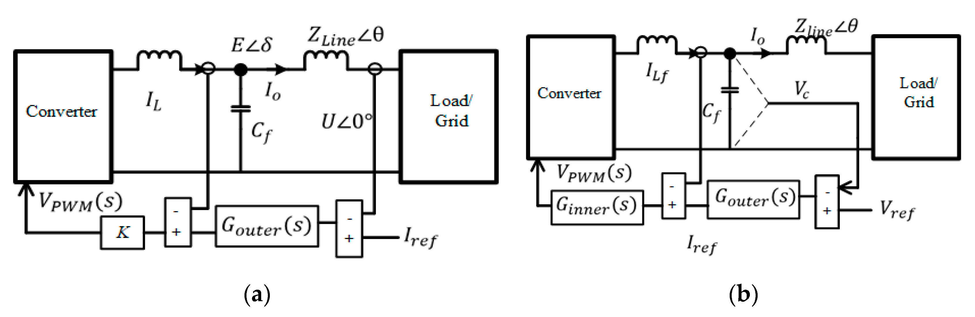
Considering the use of quasi-PR controllers in the three-phase inverter, the control structure in one axis is the same as a single-phase inverter, which simplifies the analysis. The structures of CCM and VCM are quite similar to each other with the exception of the reference signals. A block diagram of the structures is presented in
Figure 2.
As shown in
Figure 2a, the control loop of CCM is quite simple. However, its performance relies largely on the state of the grid. When the inverter is connected to the weak grid, such as the microgrid in CCM, the disturbance from the grid affects the inverter’s performance considerably. Spikes may appear when the grid voltage changes. Because stability has to be taken into consideration, inverters connecting to the microgrid are expected to be able to maintain the voltage of the microgrid [
26]. In addition, as a basic demand of the distributed generation system, the inverter must be able to operate in both islanded and grid-connected mode. Thus, the VCM, which is shown in
Figure 2b, is a more appropriate control strategy to be investigated. To introduce the detailed analysis, the system block is presented in
Figure 3.
The following transfer function of the system can be obtained:
In Equation (9), is the system’s output voltage, is the reference voltage signal, and is the system’s output current. and represent the impedance of the capacitor and the inductor, respectively. and represent the controller of the voltage and the controller of the current, respectively.
From Equation (9) it can be concluded that the output voltage relates to the reference voltage and the output current. The block can be substituted by the two-terminal Thevenin equivalent circuit as:
where
is the gain of the reference voltage,
is the equivalent impedance of the system, and
is the load current. From Equation (10) it can be concluded that the inverter can be regarded as the controllable voltage source, which has been applied in the conventional droop control. Its equivalent circuit is shown in
Figure 4.
As mentioned before, the signals existing in the system are mixtures of different frequency. Equation (10) can be rewritten as follows:
The k represents the harmonic order of the signals. From Equation (11) it can be seen that the reference signal is the ideal sinusoidal signal in fundamental frequency, which does not add harmonic elements to the output voltage . Thus, the harmonic voltage merely relates to the output current. Therefore, to implement the harmonic voltage mitigation, either the decrease in the magnitude of or the addition of feedforward compensational harmonic reference signals can be adopted.
Equation (9) reveals that, in order to decrease the magnitude of the output impedance in a selected harmonic frequency, the amplitude of
existing in the outer loop should be increased. However, as [
12] has indicated, the infinite gain deteriorates the system’s stability. To cope with this issue, virtual resistance and virtual capacitance are needed. However, this strategy increases the system’s complexity and makes the virtual impedance tuning more difficult, in addition to the resonance issue and the voltage sag issue which occur with this algorithm.
Therefore, the second conclusion is a more attractive option. The algorithm proposed in this paper uses the feedforward virtual harmonic power reference to eliminate the harmonic output voltage.
4. The Proposed Droop Control Strategy to Mitigate the Harmonic Voltage
As introduced in the last section, the conventional harmonic mitigation algorithm uses feedforward signals. Considering the demand imposed on inverters applied in a distributed generation system, this algorithm has to combine droop control. Thus, to facilitate further investigation, the conventional droop control is initially analyzed.
According to the system block shown in
Figure 3, the equivalent two-terminal circuit of the converter is shown in
Figure 5.
In
Figure 5a, the variable with the subscript
f indicates that the signals are in fundamental frequency. As mentioned above, load current and load voltage contain harmonic components, which do not exist in the inverter’s output voltage. Thus, the equivalent circuit of harmonic frequent signals is shown in
Figure 5b. According to [
15], when the feedback signals of
are opposite to the load harmonic voltage, the equivalent harmonic output impedance
will be decreased:
The transfer function block of the system can be seen in
Figure 6.
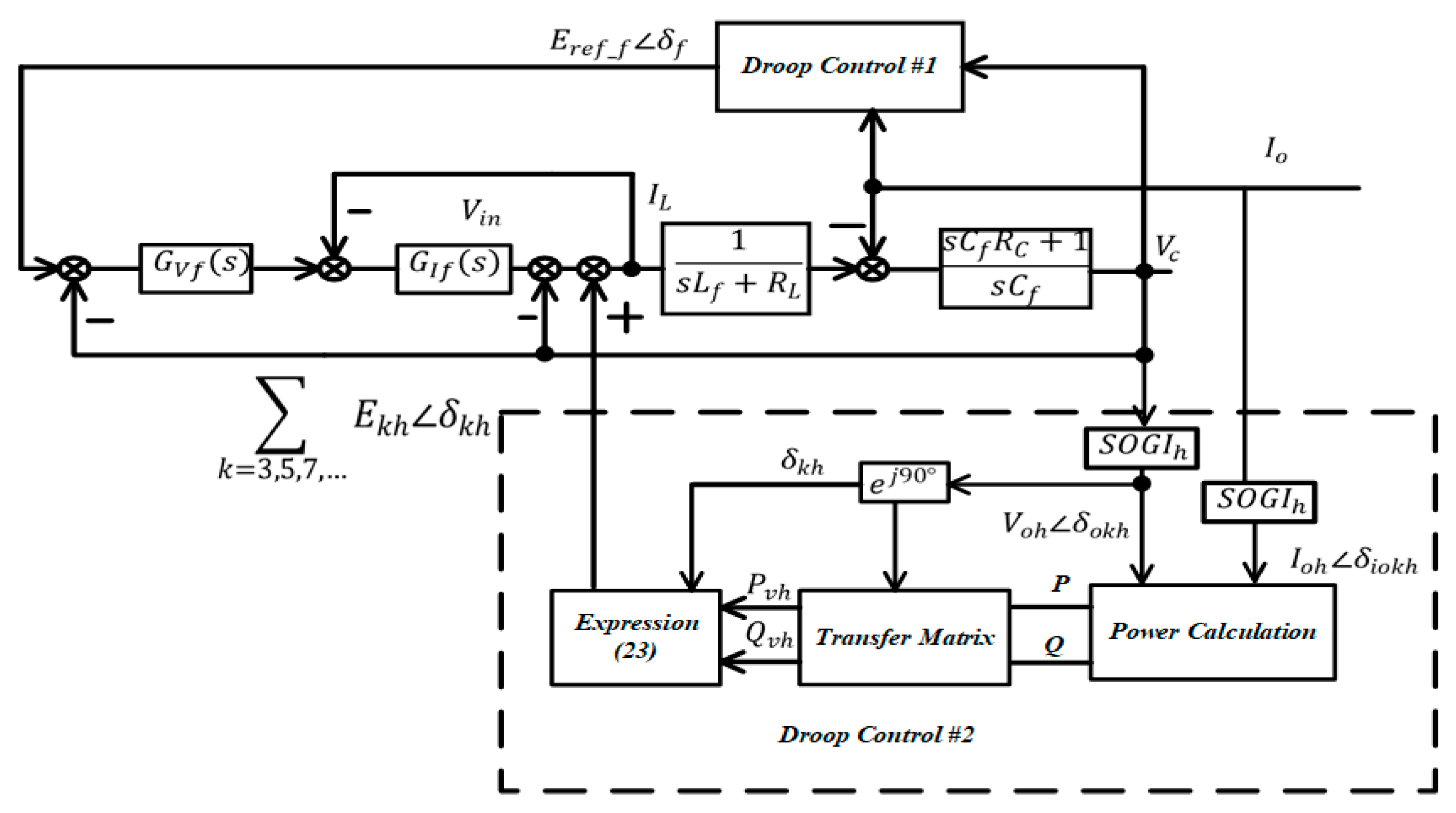
As shown in
Figure 6, the system’s main part deals with the signals in fundamental frequency, and the harmonic output voltage components are added to the system with the help of SOGIs.
In addition to the reduced output impedance, the harmonic components in the output voltage can be absorbed by the inverter. However, this algorithm cannot be applied to droop control directly, as the adjustment of output voltage relates to the system’s power. Furthermore, to make a decoupled system of droop control, the phase difference between the inverter output voltage
and the terminal voltage
is usually regarded as a small value
. However, as [
3] has indicated, the output harmonic voltage may not be in phase with the reference signal. Thus, a novel relationship between powers and the harmonic output voltage
is proposed.
Scholars have revealed that the output harmonic voltage relates to the harmonic power in a usual approach [
14]. However, that algorithm relies on the assumption that the phase difference between the inverter’s output voltage and the terminal current is quite small, which cannot be assured for every second. Thus, with the help of a virtual power concept, a harmonic virtual power algorithm is proposed to solve the output harmonic voltage issue.
First, the generalized expressions of droop control are displayed as (14), with the assumption that the line impedance is inductive:
The symbols with subscript h represent signals in harmonic frequency. As the phase difference between and may not be regarded as a small value, they are preserved as their original values and . Aiming to regulate the harmonic output voltage, the droop relationship between the power and the harmonic output voltage is expected. Thus, Equation (14) has to be modified.
To relieve the influence of the difference between the voltage angles, the orthogonal matrix
T is applied based on the virtual power algorithm:
The virtual instantaneous power
and
can be calculated as follows:
As can be seen, virtual active power
and virtual reactive power
are still coupled. Considering
and
are additional reference signals in this proposed algorithm, the voltage angle
can be manipulated. Assuming
, Equation (16) can be transferred to:
To make this a more decoupled system, one more matrix
is applied:
The new virtual powers
and
are shown. According to Equation (19) and based on the demand introduced before,
can be used for the harmonic mitigation. The relationship between them is as follows:
The droop control uses the form:
where
is used to mitigate the output harmonic voltage. The system’s control block is shown in
Figure 7.
As shown in
Figure 7,
and
are the quasi-PR controllers that merely regulate the signals in fundamental frequency, respectively.
is the fundamental component of the current flowing through the inductor. The SOGI
h represents the SOGI to exact harmonic components of the corresponding signal.
represents the system’s harmonic compensation references.
is the operator to implement the angle change of the output voltage.
is the reference signal for the voltage regulation in fundamental frequency.
In this control strategy, there are two droop control modules. Module #1 only has to control the voltage and current in fundamental frequency. The harmonic frequency signals are regulated in droop control module #2. The harmonic components are exacted and regulated by the quasi-PR controllers in the module. Thus, the signals in fundamental frequency and the harmonic frequency are decoupled and the harmonics existing in the output voltage can be mitigated.
6. Conclusions
This paper proposes an output voltage harmonic mitigation strategy that uses virtual power and harmonic droop control.
This control strategy uses a droop control algorithm, which is suitable for inverters operating in a distributed generation system. The proposed strategy does not require additional sensors nor does it change the system’s structure. The harmonic voltage and fundamental voltage are decoupled with SOGIs, allowing them to be controlled separately.
The control loop for the harmonic element is built with the help of virtual power. Unlike the conventional virtual power, the compensation values are obtained with the secondary transfer matrix .
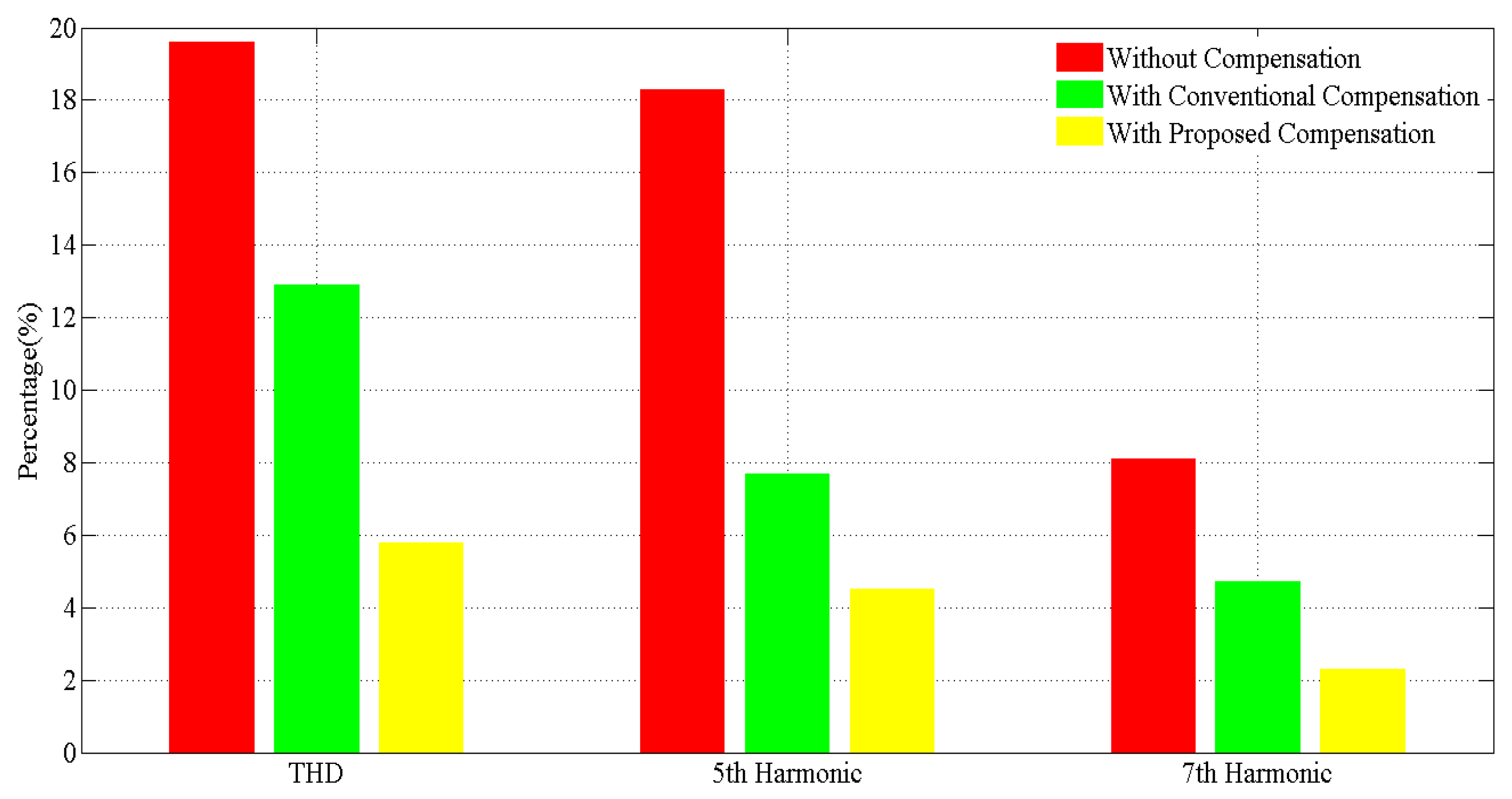
Simulation and experimental results verified the validity of this algorithm. The reduced harmonics improves the system’s stability and can be used to reduce the system’s filters, which makes the apparatus less costly and more compact.


