Design of Current Programmed Switching Converters Using Sliding-Mode Control Theory

 ,
,  , , ,
, , ,  and
and 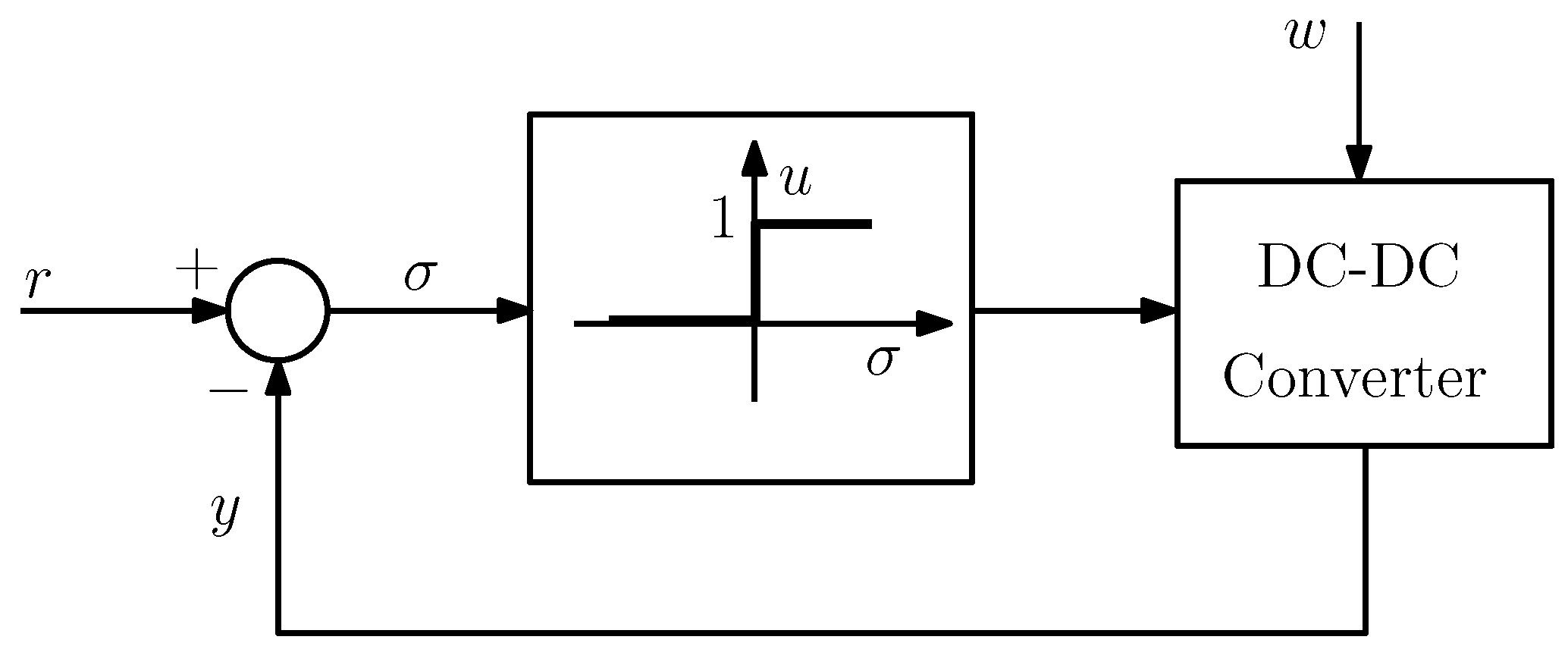
Abstract
1. Introduction
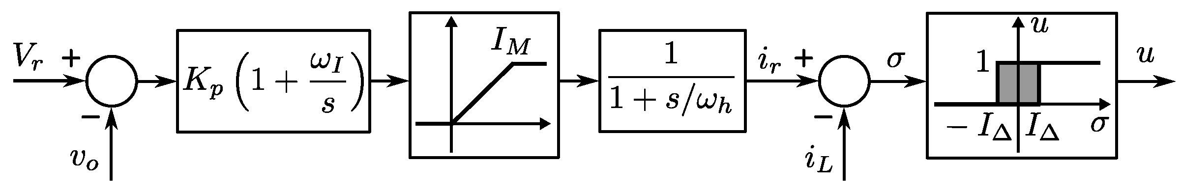
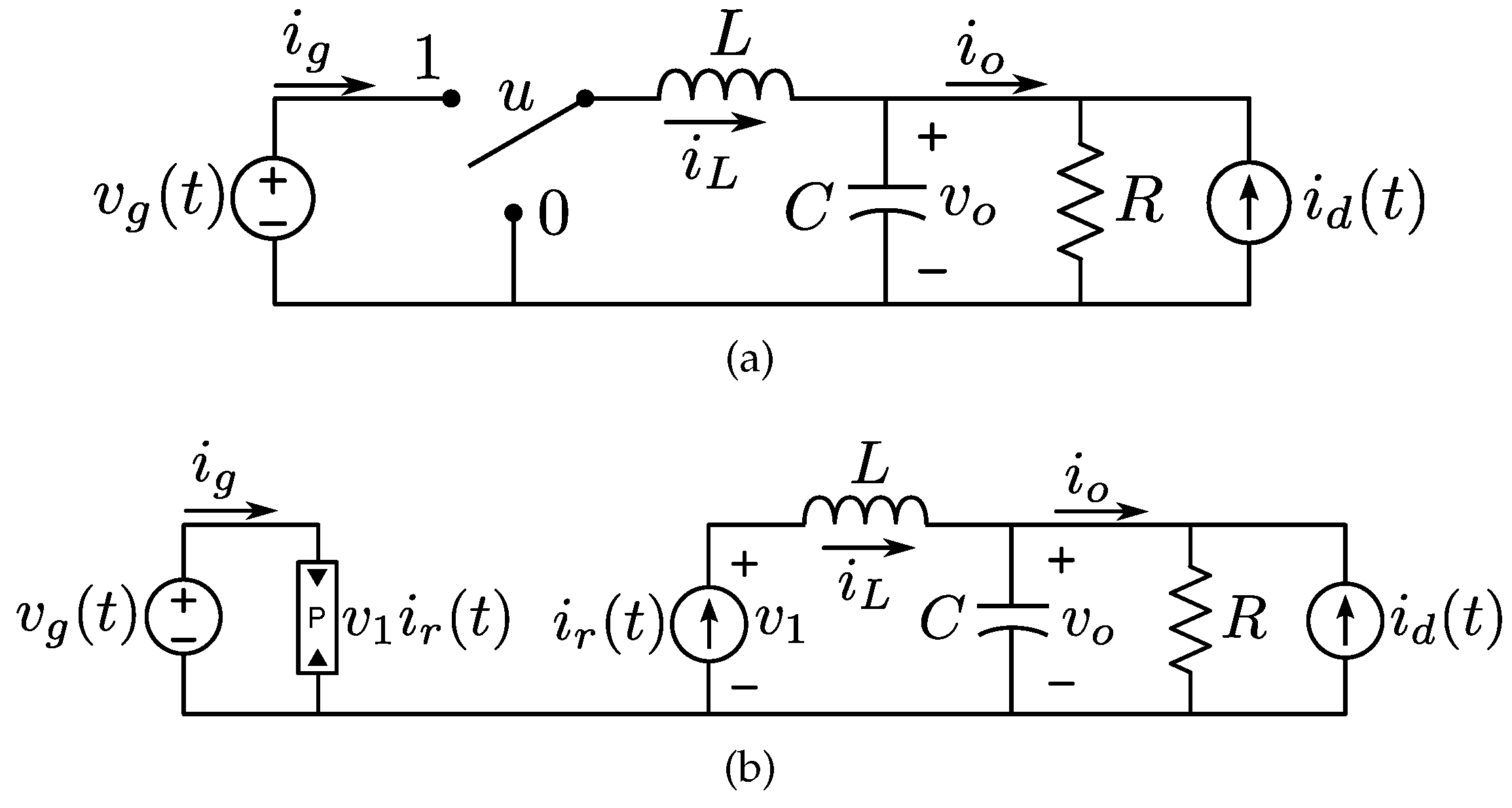
2. Sliding-Mode Control of Switching Converters Based on Two-Loop Current Mode Control
3. Practical Examples
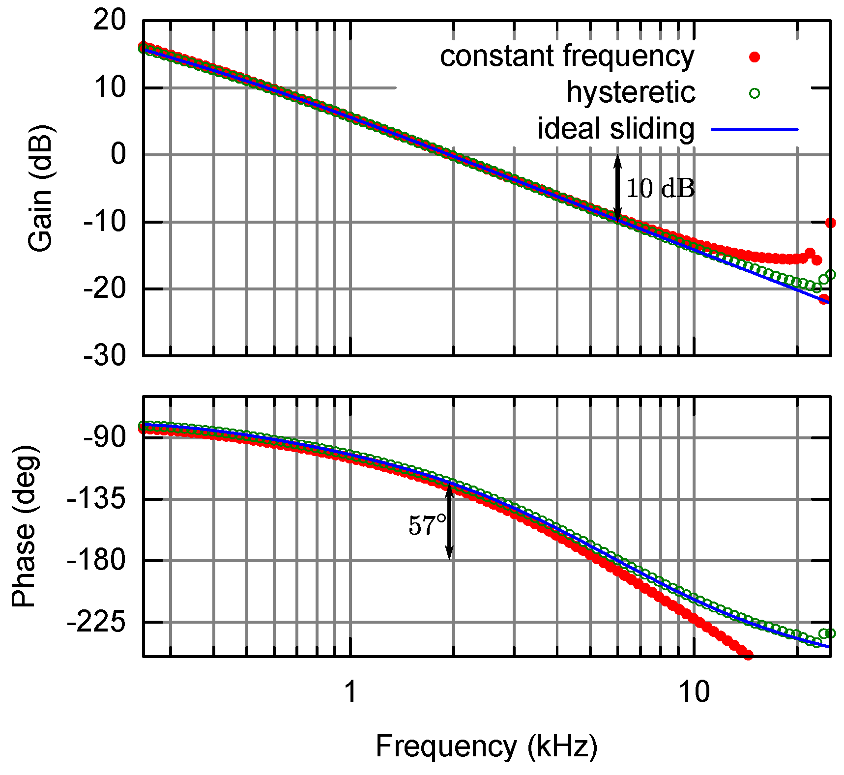
3.1. Example 1: A Boost Converter under Fixed and Variable Frequency CMC
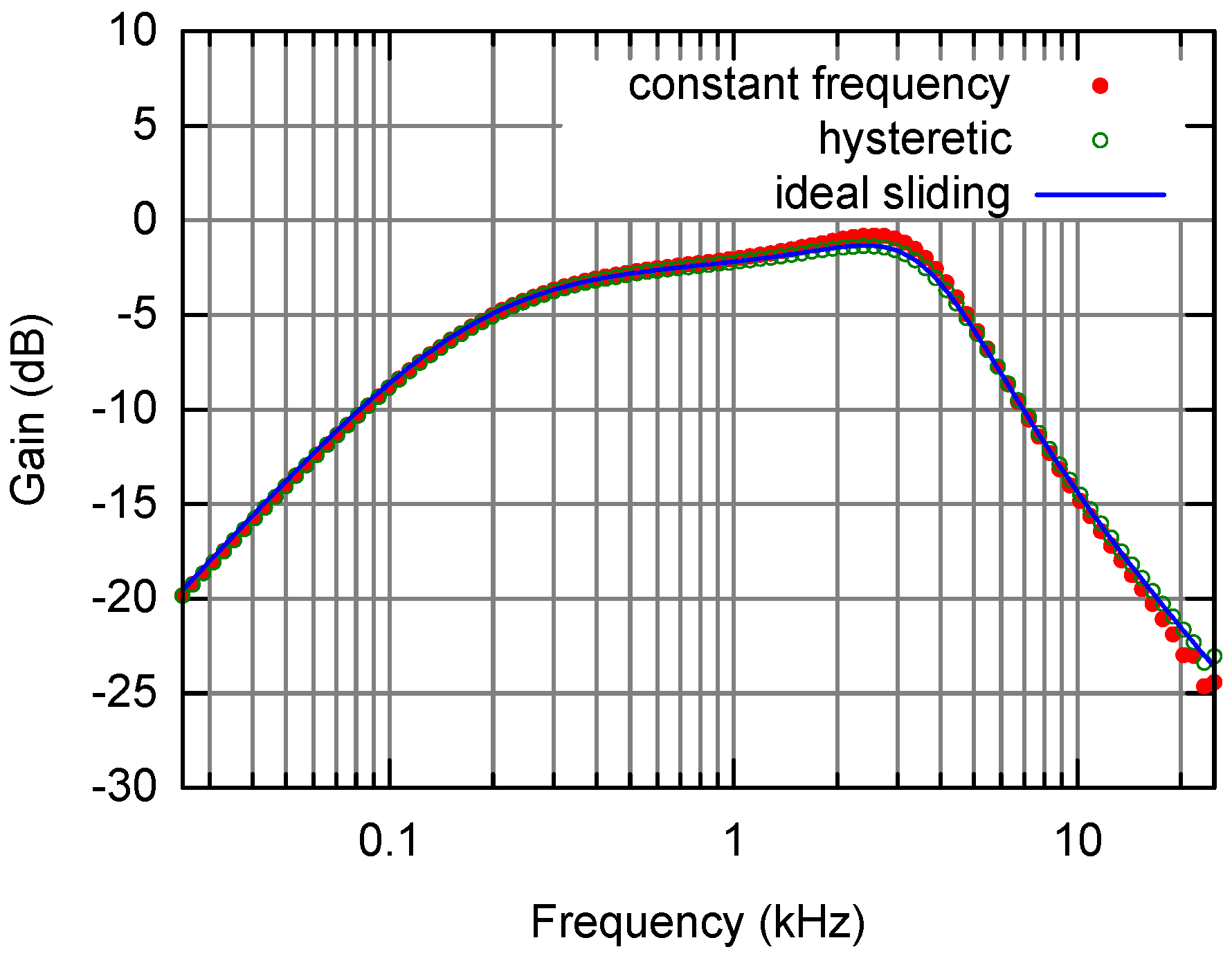
3.2. Example 2: Buck Converter under Fixed and Variable Frequency CMC
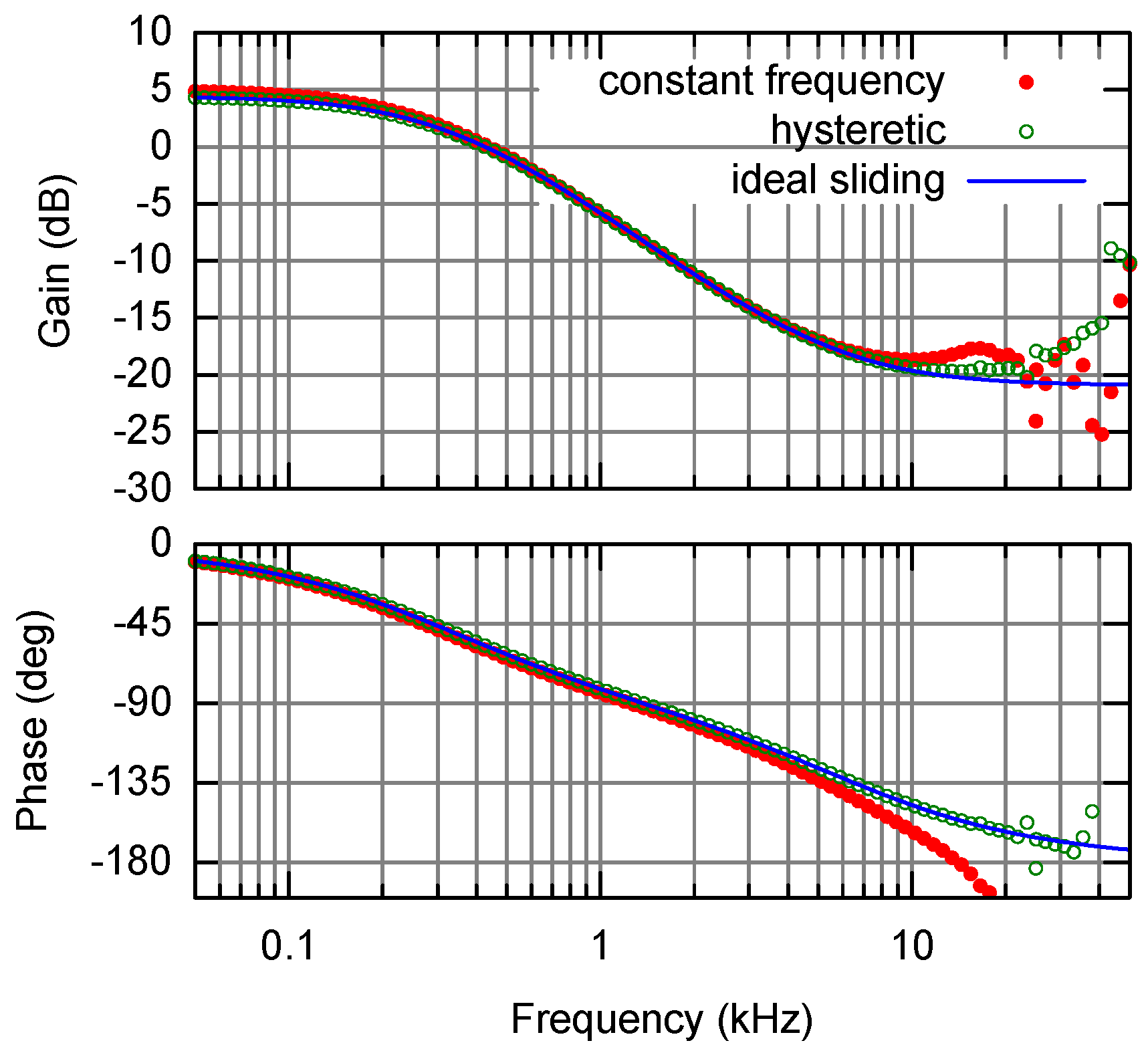
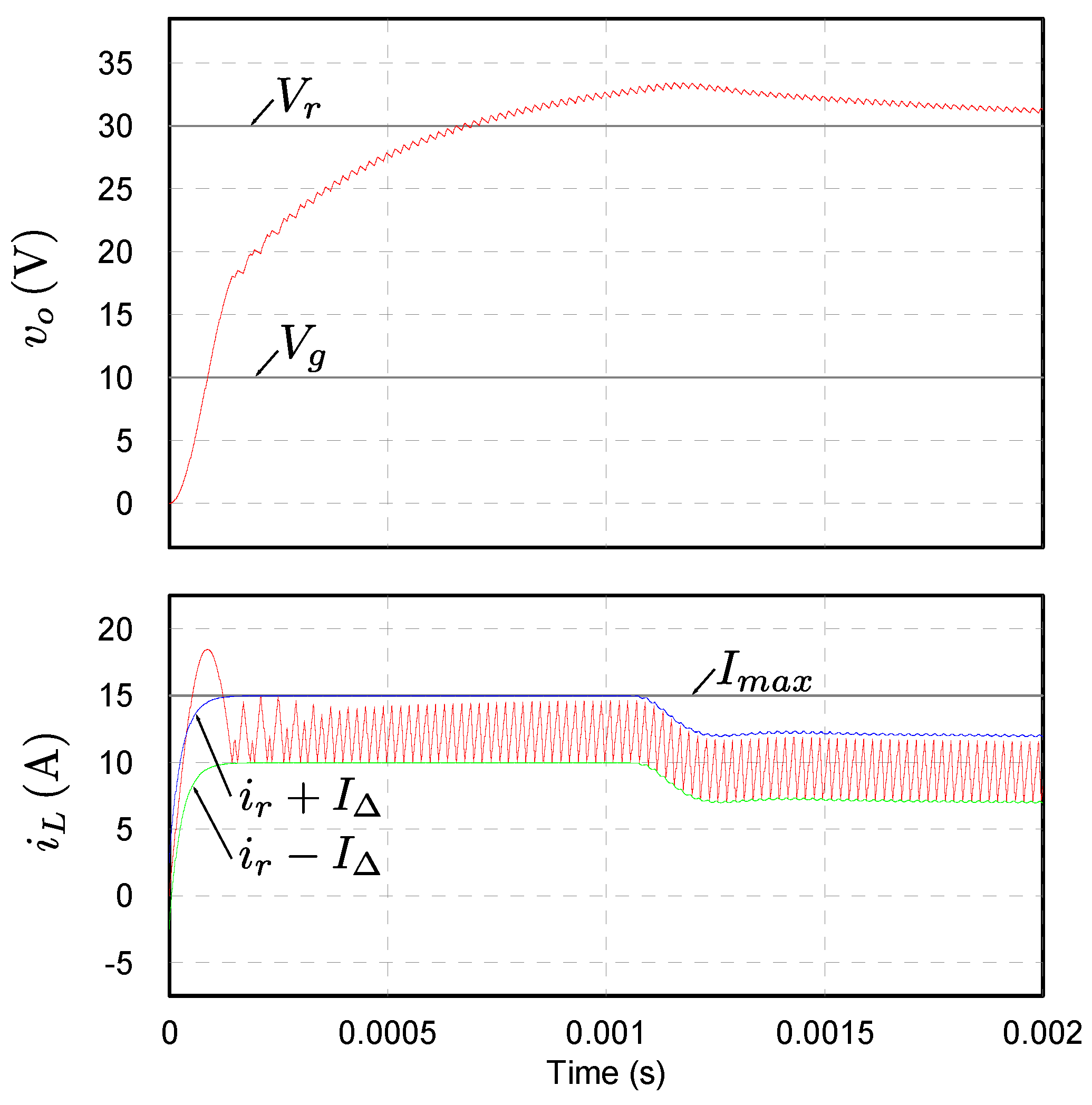
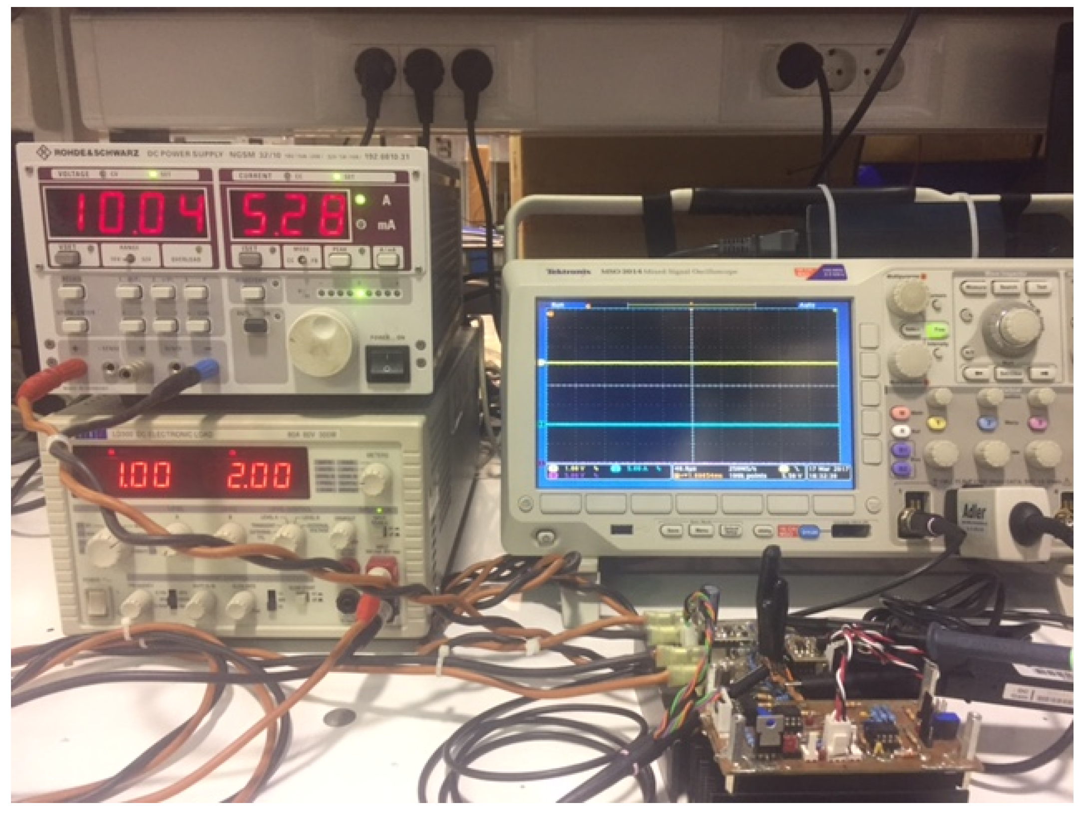
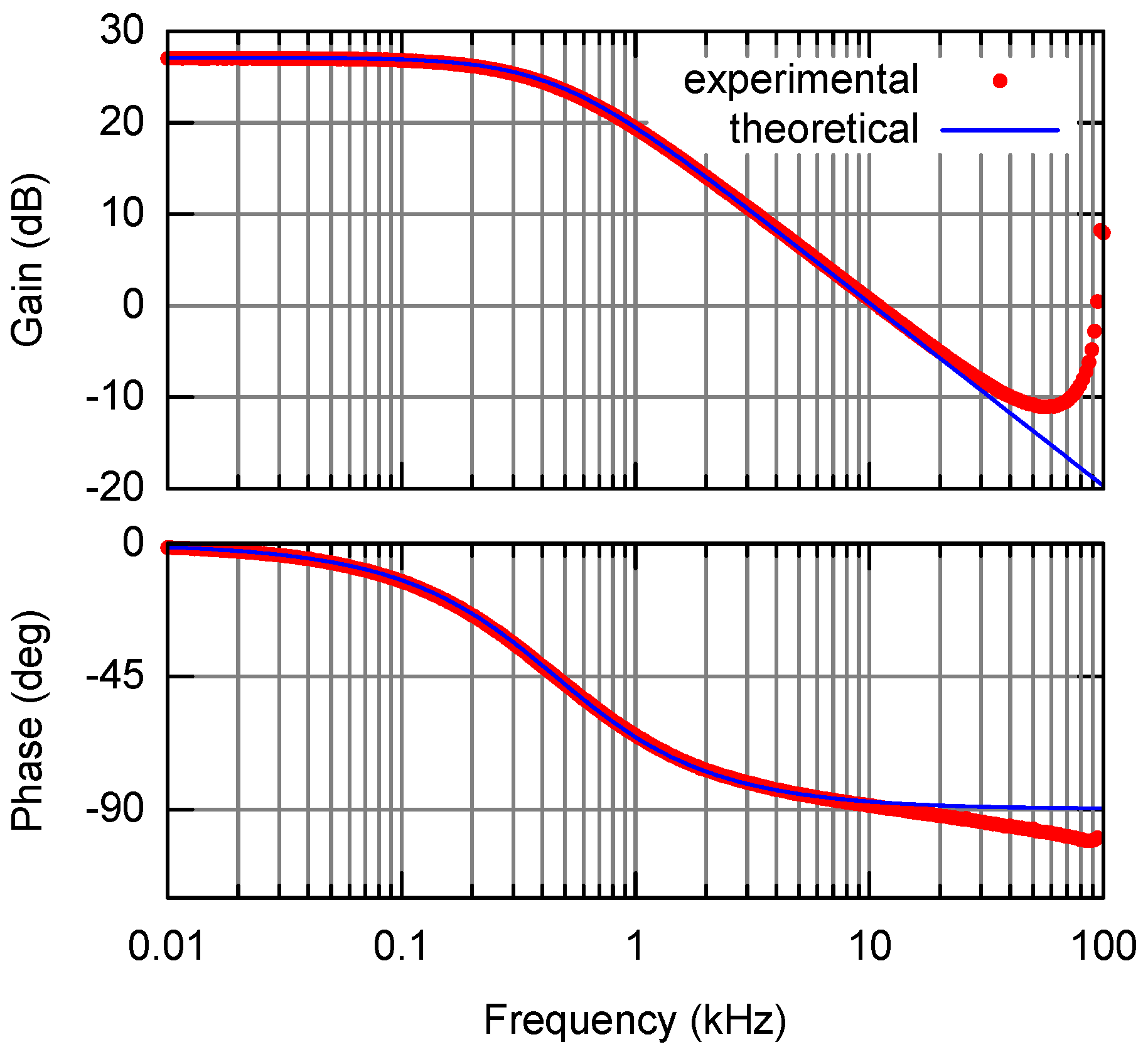
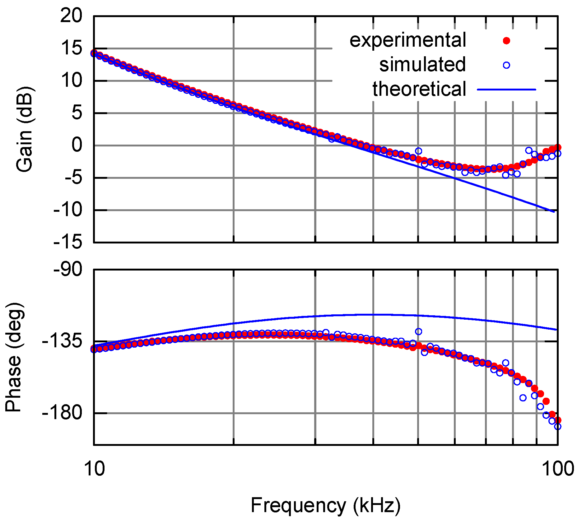
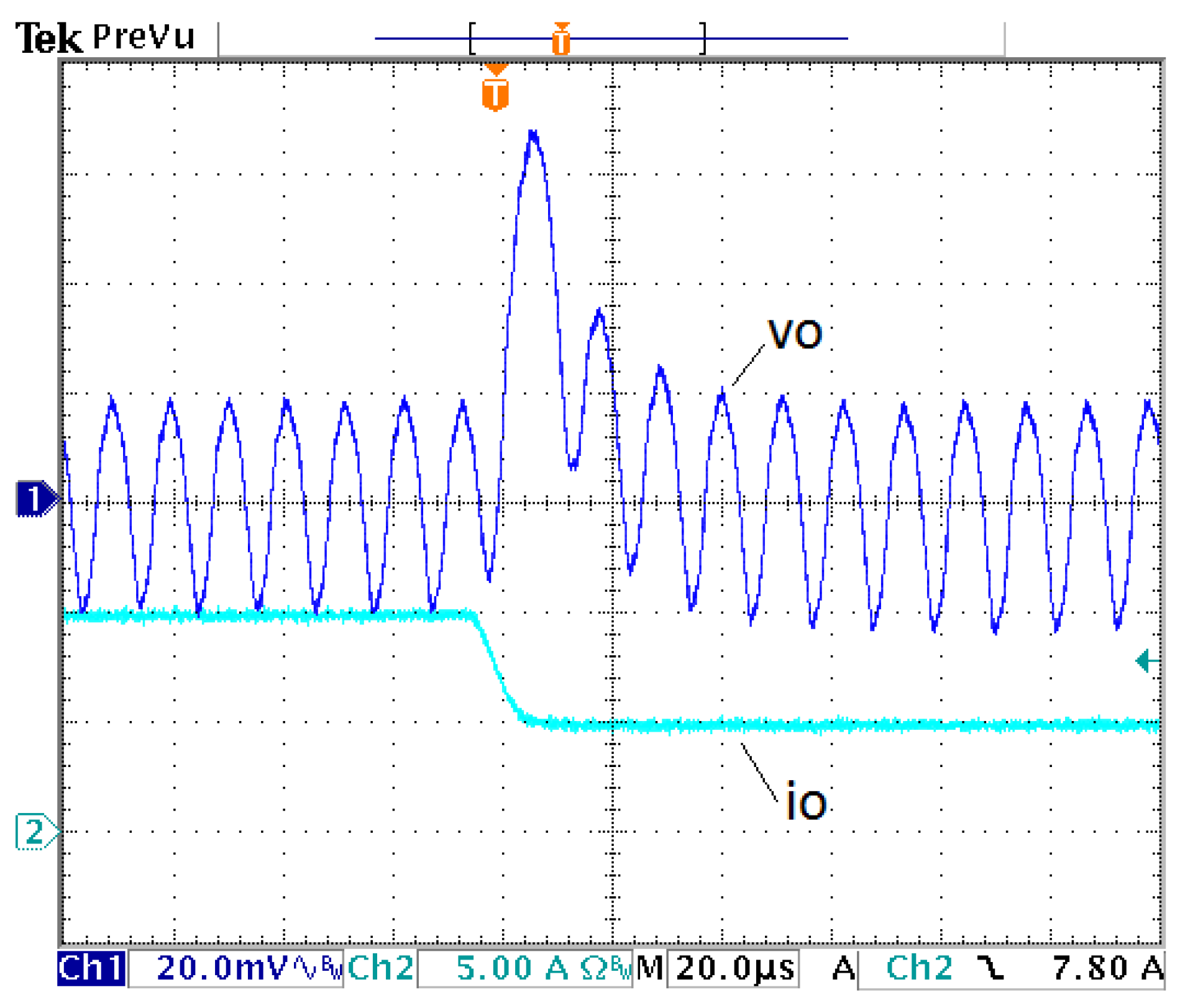
4. Experimental Results
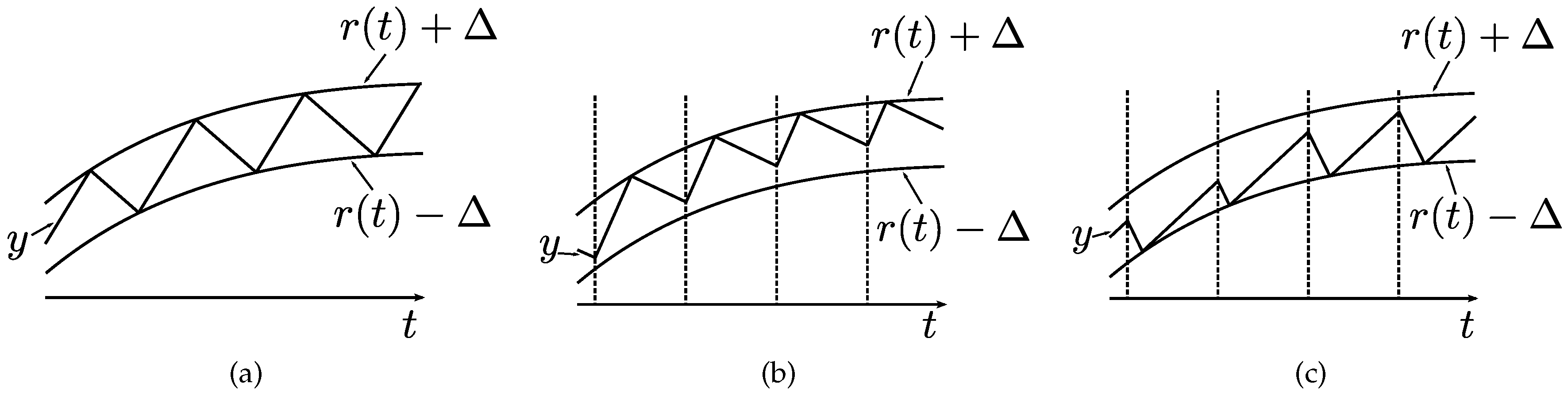
5. Discussion: Extension to Single-Loop Ripple-Based VMC Strategies
6. Conclusions
Author Contributions
Funding
Conflicts of Interest
References
- El Fadil, H.; Giri, F. Robust nonlinear adaptive control of multiphase synchronous buck power converters. Control Eng. Pract. 2009, 17, 1245–1254. [Google Scholar] [CrossRef]
- Erickson, R.W.; Maksimovic, D. Fundamentals of Power Electronics; Kluwer: Alphen aan den Rijn, The Netherlands, 2001. [Google Scholar]
- Yfoulis, C.; Giaouris, D.; Stergiopoulos, F.; Ziogou, C.; Voutetakis, S.; Papadopoulou, S. Robust constrained stabilization of boost DC-DC converters through bifurcation analysis. Control Eng. Pract. 2015, 35, 67–82. [Google Scholar] [CrossRef]
- Middlebrook, R. Topics in multiple-loop regulators and current-mode programming. IEEE Trans. Power Electron. 1987, PE-2, 109–124. [Google Scholar] [CrossRef]
- Ramos, R.; Biel, D.; Fossas, E.; Gri, R. Sliding mode controlled multiphase buck converter with interleaving and current equalization. Control Eng. Pract. 2013, 21, 737–746. [Google Scholar] [CrossRef]
- Liu, Y.-F.; Sen, P.C. Large-signal modeling of hysteretic current-programmed converters. IEEE Trans. Power Electron. 1996, 11, 423–430. [Google Scholar]
- Martinez-Salamero, L.; Garcia, G.; Orellana, M.; Lahore, C.; Estibals, B. Start-up control and voltage regulation in a boost converter under sliding-mode operation. IEEE Trans. Ind. Electron. 2013, 60, 4637–4646. [Google Scholar] [CrossRef]
- Deisch, C.W. Simple switching control method changes power converter into a current source. In Proceedings of the PESC’78, Power Electronics Specialists Conference, Syracuse, NY, USA, 13–15 June 1978; pp. 300–306. [Google Scholar]
- Redl, R.; Sokal, N. Current-mode control, five different types, used with the three basic classes of power converters-small-signal ac and large-signal dc characterization, stability requirements, and implementation of practical circuits. In Proceedings of the PESC’85 Record, 16th Annual IEEE, Toulouse, France, 24–28 June 1985; pp. 771–785. [Google Scholar]
- Perreault, D.; Verghese, G.C. Time-varying effects and averaging issues in models for current-mode control. IEEE Trans. Power Electron. 1997, 12, 453–461. [Google Scholar] [CrossRef]
- Ridley, R. A new, continuous-time model for current-mode contro. IEEE Trans. Power Electron. 1991, 6, 271–280. [Google Scholar] [CrossRef]
- Tan, F.; Middlebrook, R. A unified model for current-programmed converters. IEEE Trans. Power Electron. 1995, 10, 397–408. [Google Scholar] [CrossRef]
- Yan, Y.; Lee, F.; Mattavelli, P. Comparison of small signal characteristics in current mode control schemes for point-of-load buck converter applications. IEEE Trans. Power Electron. 2013, 28, 3405–3414. [Google Scholar] [CrossRef]
- Li, J.; Lee, F. New modeling approach and equivalent circuit representation for current-mode control. IEEE Trans. Power Electron. 2010, 25, 1218–1230. [Google Scholar]
- Babaa, I.; Wilson, T.; Yu, Y. Analytic solutions of limit cycles in a feedback-regulated converter system with hysteresis. IEEE Trans. Autom. Control 1968, 13, 524–531. [Google Scholar] [CrossRef]
- Schweitzer, B.P.; Rosenstein, A.B. Free Running-Switching Mode Power Regulator: Analysis and Design. IEEE Trans. Aerosp. 1964, 2, 1171–1180. [Google Scholar] [CrossRef]
- Huerta, S.; Soto, A.; Alou, P.; Oliver, J.; Garcia, O.; Cobos, J. Advanced control for very fast DC-DC converters based on hysteresis of the Cout current. IEEE Trans. Circuits Syst. I Regular Pap. 2013, 60, 1052–1061. [Google Scholar] [CrossRef]
- Ki, W.-H.; Lai, K.-M.; Zhan, C. Charge balance analysis and state transition analysis of hysteretic voltage mode switching converters. IEEE Trans. Circuits Power Syst. 2011, 58, 1142–1152. [Google Scholar] [CrossRef]
- Wen, Y.; Trescases, O. Analysis and comparison of frequency stabilization loops in self-oscillating current mode dc-dc converters. IEEE Trans. Power Electron. 2013, 28, 4753–4766. [Google Scholar] [CrossRef]
- Castilla, M.; Guerrero, J.; Matas, J.; Miret, J.; Sosa, J. Comparative study of hysteretic controllers for single-phase voltage regulators. IET Power Electron. 2008, 1, 132–143. [Google Scholar] [CrossRef]
- Atre, S.R.; Lele, V.P. Analytic application of Tsypkin’s method relay with hysteresis and dead zone. Proc. Inst. Electr. Eng. 1977, 124, 1241–1242. [Google Scholar] [CrossRef]
- Barrado, J.A.; El Aroudi, A.; Valderrama-Blavi, H.; Calvente, J.; Martinez-Salamero, L. Analysis of a self-oscillating bidirectional DC-DC converter in battery energy storage applications. IEEE Trans. Power Deliv. 2012, 27, 1292–1300. [Google Scholar] [CrossRef]
- Tsypkin, Y.Z. Relay Control Systems; Cambridge Univ. Press: Cambridge, UK, 1984. [Google Scholar]
- Boiko, I. Variable-structure PID controller for level process. Control Eng. Pract. 2013, 21, 700–707. [Google Scholar] [CrossRef]
- Utkin, V.; Guldner, J.; Shi, J. Sliding Mode Control in Electro-Mechanical Systems, (Automation and Control Engineering); CRC Press: Boca Raton, FL, USA, 2009. [Google Scholar]
- Filippov, A.F. Differential equations with discontinuous right-hand side. Am. Math. Soc. Transl. 1964, 42, 199–231. [Google Scholar]
- Utkin, V.I. Sliding Modes in Control and Optimization; Springer-Verlag: Berlin, Germany, 1992. [Google Scholar]
- Sira-Ramirez, H. Sliding motions in bilinear switched networks. IEEE Trans. Circuits Syst. 1987, 34, 919–933. [Google Scholar] [CrossRef]
- Bilalovic, F.; Music, O.; Sabanovic, A. Buck converter regulator operating in the sliding mode. In Proceedings of the 7th Internatinal PCI Conference, Orlando, FL, USA, 19–21 April 1983; pp. 331–340. [Google Scholar]
- Malesani, L.; Rossetto, L.; Spiazzi, G.; Tenti, P. Performance optimization of Cuk converters by sliding-mode control. IEEE Trans. Power Electron. 1995, 10, 302–309. [Google Scholar] [CrossRef]
- Spiazzi, G.; Mattavelli, P. Sliding-mode control of switched-mode power supplies. In The Power Electronics Handbook; Chapter 8; Lappeenranta University of Technology: Lappeenranta, Finland, 2002. [Google Scholar]
- Tan, S.-C.; Lai, Y.; Cheung, M.; Tse, C. On the practical design of a sliding mode voltage controlled buck converter. IEEE Trans. Power Electron. 2005, 20, 425–437. [Google Scholar] [CrossRef]
- Tan, S.-C.; Lai, Y.; Tse, C.; Cheung, M. Adaptive feedforward and feedback control schemes for sliding mode controlled power converters. IEEE Trans. Power Electron. 2006, 21, 182–192. [Google Scholar]
- Chen, Z.; Gao, W.; Hu, J.; Ye, X. Closed-loop analysis and cascade control of a nonminimum phase boost converter. IEEE Trans. Power Electron. 2011, 26, 1237–1252. [Google Scholar] [CrossRef]
- Chen, Z. PI and sliding mode control of a Ćuk converter. IEEE Trans. Power Electron. 2012, 27, 3695–3703. [Google Scholar] [CrossRef]
- Komurcugil, H. Non-singular terminal sliding-mode control of DC-DC buck converters. Control Eng. Pract. 2013, 21, 321–332. [Google Scholar] [CrossRef]
- Singh, P.; Hote, Y.; Garg, M. Comments on PI and sliding mode control of a Cuk converter. IEEE Trans. Power Electron. 2014, 29, 1551–1552. [Google Scholar] [CrossRef]
- Sira-Ramirez, H.; Luviano-Juarez, A.; Romero, J.C. Robust input-output sliding mode control of the buck converter. Control Eng. Pract. 2013, 21, 671–678. [Google Scholar] [CrossRef]
- Ramos, R.; Biel, D.; Fossas, E.; Guinjoan, F. Interleaving quasi-sliding-mode control of parallel-connected buck-based inverters. IEEE Trans. Ind. Electron. 2008, 55, 3865–3873. [Google Scholar] [CrossRef]
- Cid-Pastor, A.; Martinez-Salamero, L.; Alonso, C.; Estibals, B.; Alzieu, J.; Schweitz, G.; Shmilovitz, D. Analysis and design of power gyrators in sliding-mode operation. IEE Proc. Electr. Power Appl. 2005, 152, 821–826. [Google Scholar] [CrossRef]
- Haroun, R.; Cid-Pastor, A.; El Aroudi, A.; Martinez-Salamero, L. Synthesis of canonical elements for power processing in dc distribution systems using cascaded converters and sliding-mode control. IEEE Trans. Power Electron. 2014, 29, 1366–1381. [Google Scholar] [CrossRef]
- Cid-Pastor, A.; Giral, R.; Calvente, J.; Utkin, V.; Martinez-Salamero, L. Interleaved converters based on sliding-mode control in a ring configuration. IEEE Trans. Circuits Syst. I Regular Pap. 2011, 58, 2566–2577. [Google Scholar] [CrossRef]
- Utkin, V. Sliding mode control of dc/dc converters. J. Frank. Inst. 2013, 350, 2146–2165. [Google Scholar] [CrossRef]
- Cid-Pastor, A.; Martinez-Salamero, L.; El Aroudi, A.; Giral, R.; Calvente, J.; Leyva, R. Synthesis of loss-free resistors based on sliding-mode control and its applications in power processing. Control Eng. Pract. 2013, 21, 689–699. [Google Scholar] [CrossRef]
- Vidal-Idiarte, E.; Martinez-Salamero, L.; Guinjoan, F.; Calvente, J.; Gomariz, S. Sliding and fuzzy control of a boost converter using an 8-bit microcontroller. IET Electr. Power Appl. 2004, 151, 5–11. [Google Scholar] [CrossRef]
- Vidal-Idiarte, E.; Martínez-Salamero, L.; Calvente, J.; Romero, A. An H∞ control strategy for switching converters in sliding-mode current control. IEEE Trans. Power Electron. 2006, 21, 553–556. [Google Scholar] [CrossRef]
- Mattavelli, P.; Rossetto, L.; Spiazzi, G. Small-signal analysis of DC-DC converters with sliding mode control. IEEE Trans. Power Electron. 1997, 12, 96–102. [Google Scholar] [CrossRef]
- Chan, M.P.; Mok, P.K.T. A monolithic 2nd-order boundary controller for buck converter with fast transient response. In Proceedings of the 2010 IEEE Asia Pacific Conference on Circuits and Systems, Kuala Lumpur, Malaysia, 6–9 December 2010. [Google Scholar]
- Biel, D.; Fossas, E. SMC applications in power electronics. Var. Struct. Syst. Princ. Implementation 2004, 66, 265–293. [Google Scholar]
- Silva, J.; Paulo, S. Fixed frequency sliding mode modulator for current mode PWM inverters. In Proceedings of the 24th Annual IEEE Power Electronics Specialist Conference—PESC ’93, Seattle, WA, USA, 20–24 June 1993; pp. 623–629. [Google Scholar]
- Singer, S.; Erickson, R. Power-source element and its properties. IEE Proc. Circuits Devices Syst. 1994, 141, 220–226. [Google Scholar] [CrossRef]
- Sira-Ramirez, H.; Silva-Ortigoza, R. Control Design Techniques in Power Electronics Devices, Power Systems Series; Springer: London, UK, 2006. [Google Scholar]
- Doyle, J.; Francis, B.; Tannenbaum, A. Feedback Control Theory; Macmillan Publishing Co.: Basingstoke, UK, 1990. [Google Scholar]
- Goder, D.; Pelletier, W.R. V2 Architecture Provides Ultra-Fast Transient Response in Switch Power Supplies; Intertect International: Las Vegas, NV, USA, 1996; pp. 19–23. [Google Scholar]
- Redl, R.; Sun, J. Ripple-based control of switching regulators: an overview. IEEE Trans. Power Electron. 2009, 24, 2669–2680. [Google Scholar] [CrossRef]
- Sun, J. Characterization and performance comparison of ripple-based control for voltage regulator modules. IEEE Trans. Power Electron. 2006, 21, 346–353. [Google Scholar]
- Del Viejo, M.; Alou, P.; Oliver, J.A.; García, O.; Cobos, J.A. V2IC control: A novel control technique with very fast response under load and voltage steps. In Proceedings of the 2011 Twenty-Sixth Annual IEEE Applied Power Electronics Conference and Exposition (APEC), Fort Worth, TX, USA, 6–11 March 2011. [Google Scholar]
- Cortes, J.; Svikovic, V.; Alou, P.; Oliver, J.; Cobos, J.A. V1 concept: Designing a voltage mode control as current mode with near time-optimal response for Buck-type converters. IEEE Trans. Power Electron. 2015, 30, 5829–5841. [Google Scholar] [CrossRef]
- Chen, M.; Zhao, M.; Wu, X. A fixed-frequency fast transient response DC-DC controller for VRMs. J. Semiconduct. 2013, 34, 125002. [Google Scholar] [CrossRef]
- Yan, Y.; Lee, F.C.; Mattavelli, P.; Liu, P.H. I2 average current mode control for switching converters. IEEE Trans. Power Electron. 2014, 29, 2027–2036. [Google Scholar] [CrossRef]
- Pitel, G.E.; Krein, P.T. Minimum-time transient recovery for DC-DC converters using raster control surfaces. IEEE Trans. Power Electron. 2009, 12, 2692–2703. [Google Scholar] [CrossRef]
- Kapat, S.; Krein, P.T. Improved time optimal control of a buck converter based on capacitor current. IEEE Trans. Power Electron. 2012, 27, 1444–1454. [Google Scholar] [CrossRef]
- Kapat, S.; Krein, P.T. Formulation of PID control for DC-DC converters based on capacitor current: A geometric context. IEEE Trans. Power Electron. 2012, 27, 1424–1432. [Google Scholar] [CrossRef]
- Onwuchekwa, C.N.; Kwasinski, A. Analysis of boundary control for buck converters with instantaneous constant-power loads. IEEE Trans. Power Electron. 2010, 2, 2018–2032. [Google Scholar] [CrossRef]
- Santi, E.; Monti, A.; Li, D.; Proddutur, K.; Dougal, R.A. Synergetic control for DC-DC boost converter: Implementation options. IEEE Trans. Ind. Appl. 2003, 39, 1803–1813. [Google Scholar] [CrossRef]


© 2018 by the authors. Licensee MDPI, Basel, Switzerland. This article is an open access article distributed under the terms and conditions of the Creative Commons Attribution (CC BY) license (http://creativecommons.org/licenses/by/4.0/).
Share and Cite
Calvente, J.; El Aroudi, A.; Giral, R.; Cid-Pastor, A.; Vidal-Idiarte, E.; Martínez-Salamero, L. Design of Current Programmed Switching Converters Using Sliding-Mode Control Theory. Energies 2018, 11, 2034. https://doi.org/10.3390/en11082034
Calvente J, El Aroudi A, Giral R, Cid-Pastor A, Vidal-Idiarte E, Martínez-Salamero L. Design of Current Programmed Switching Converters Using Sliding-Mode Control Theory. Energies. 2018; 11(8):2034. https://doi.org/10.3390/en11082034
Chicago/Turabian StyleCalvente, Javier, Abdelali El Aroudi, Roberto Giral, Angel Cid-Pastor, Enric Vidal-Idiarte, and Luis Martínez-Salamero. 2018. "Design of Current Programmed Switching Converters Using Sliding-Mode Control Theory" Energies 11, no. 8: 2034. https://doi.org/10.3390/en11082034
APA StyleCalvente, J., El Aroudi, A., Giral, R., Cid-Pastor, A., Vidal-Idiarte, E., & Martínez-Salamero, L. (2018). Design of Current Programmed Switching Converters Using Sliding-Mode Control Theory. Energies, 11(8), 2034. https://doi.org/10.3390/en11082034