1. Introduction
The electricity consumption growth and environmental concerns favor the proliferation of renewable sources and distributed generation (DG) integration into the grid [
1]. This paradigm shift in the electrical system power generation introduces the need for the modernization of the grid infrastructure, demanding bidirectional power flow, remote monitoring, control and intelligent management of the entire system [
2]. This scenario encourages the consolidation of distribution level microgrids, which, through the use of energy storage, can smooth the intermittent nature of renewable energy sources and provide the utility operator real-time control over the power exchanged between the microgrid and the distribution grid. On the consumer side, microgrids are able to mitigate disturbances and failures from the distribution system, enhancing power quality and energy availability.
In this scenario, the function and structure of power transformers must be readdressed. Although these elements present high reliability, robustness and efficiency, as the outcome of more than a century of technological development, their passive structure is not enough for the new electrical system demands [
3,
4]. The evolution of power electronics enables the development of an active transformer, that not only performs the conversion of voltage levels, but also promotes ancillary services such as reactive current injection, harmonic compensation and voltage regulation, in addition to compensating for disturbances and managing the power routing between power distribution systems [
3,
5,
6,
7,
8,
9]. Solid State Transformers (SST), as these new elements are being referred to, also provide volume and weight reduction, when compared to their passive counterparts [
10]; hence, they emerge as natural candidates for implementing the interface between microgrids and medium voltage distribution networks [
1,
11].
The literature describes several structures capable of implementing the features of a SST [
12,
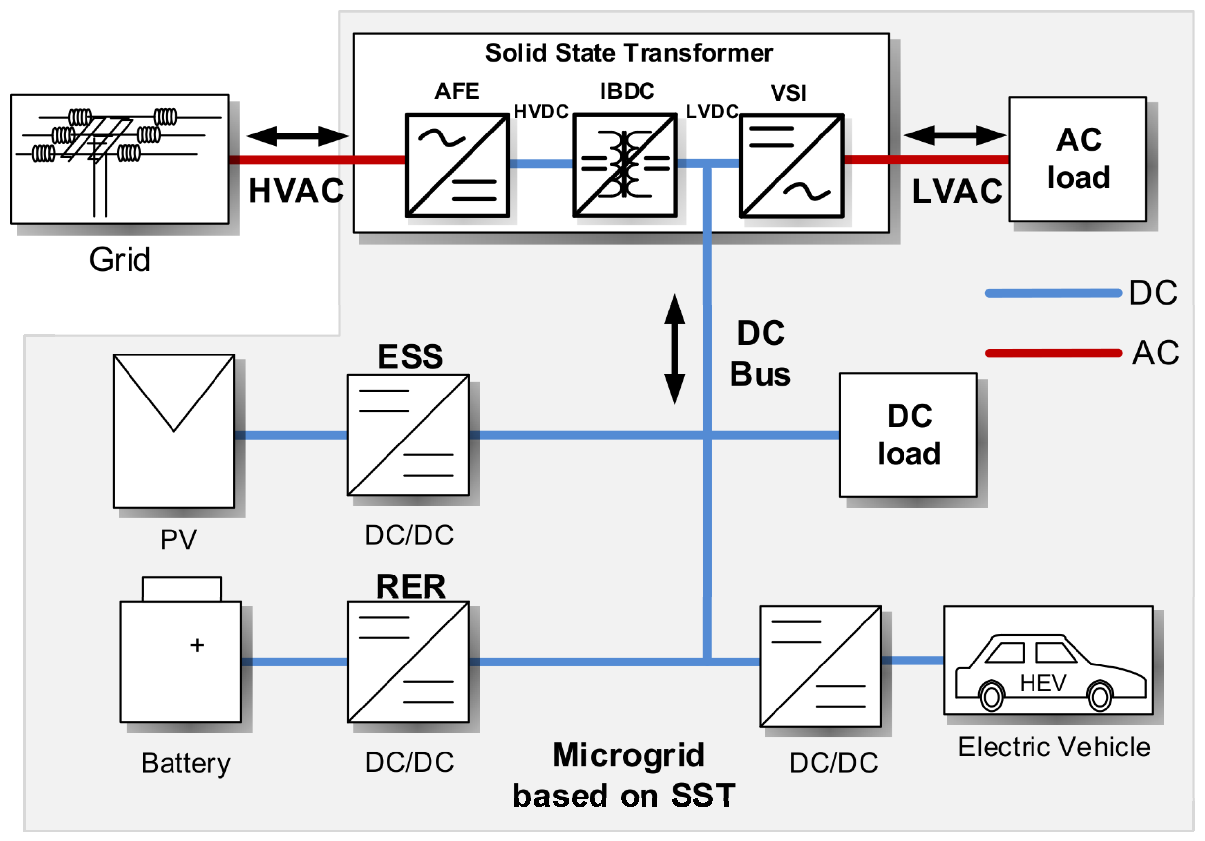
13]. However, for microgrid applications, the three-stage topology, as shown in
Figure 1, is more attractive. In this structure, the interface with the medium voltage bus is performed by an active front-end rectifier (AFE), which regulates the high voltage DC link (HVDC). An isolated bidirectional DC/DC (IBDC) converter then produces a low voltage bus (LVDC) and a DC/AC converter interfaces it with a low voltage AC grid [
14,
15]. It is observed that the SST can behave like a three port converter (HVAC, LVDC and LVAC), allowing power routing between the medium voltage distribution system and the AC and DC sub-grids of a local microgrid.
One of the main limitations regarding the selection of power converter topologies for the implementation of each SST stage is in the rectifier, which usually is coupled to a medium voltage grid with line voltage of about 10 kV. In this case, the voltage level of the HVDC link exceeds the blocking capacity offered by current semiconductor devices and imposes severe challenges in the construction of high frequency transformers. Thus, the association of series/parallel converters becomes a necessity to meet the voltage and power requirements of SST [
13].
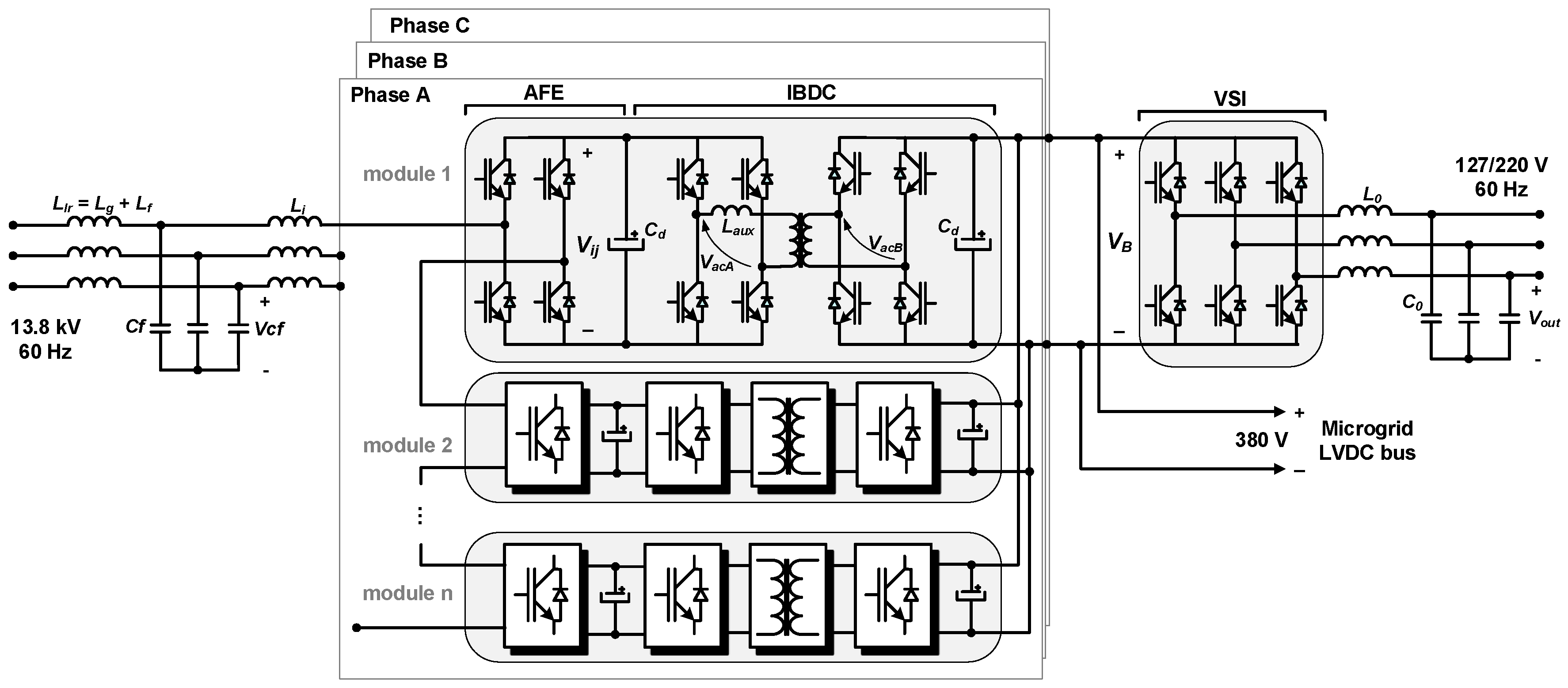
Figure 2 presents a solution to this issue, where AFE and IBDC stages are integrated into an Isolated Front-End (IFE) power module, composed by the association of a Full-bridge (FB) and a Dual Active Bridge (DAB) converter, featuring a series connection at the input and parallel at the output (Input Series-Output Parallel (ISOP)) [
16]. Due to low voltage levels employed in the LVDC bus, a central Voltage Source Inverter (VSI) is used as LVAC grid interface.
The structure shown in
Figure 2 allows the HVDC voltage to be distributed between the modules of one phase, enabling the use of power switches with lower voltage blocking capability. In addition, the multilevel structure of the input rectifier allows the use of low switching frequencies at the rectifier, which reduces switching losses and at the same time reduces the requirements on passive filters at the HVAC bus interface. However, differences between modules, caused by component tolerance, unbalanced load, etc., give rise to HVDC voltage imbalance and uneven power sharing [
17]. This condition can cause overvoltage and overload problems, increasing the stress on the power switches, which can lead to severe damage on the SST. Therefore, it is crucial to embed voltage and power balancing functions in the SST control system.
The literature provides several proposals to deal with the problem of balancing voltage and power between the modules of the converter [
14,
15,
17,
18,
19,
20]. However, most of these studies describe solutions based on a centralized control architecture, i.e., there is a need to measure individual quantities of each module, for example, HVDC bus voltage, DAB output current, etc., which will be informed to a controller that will change the FB or DAB duty cycles to achieve voltage and power balance goals. Considering that the number of SST modules can be high depending on the blocking capability of the switches used, a centralized control strategy may demand the processing of a large volume of information, requiring the use of high-speed communication links and complex signal processing and conditioning systems, compromising cost and reliability. In this sense, the use of a decentralized balancing strategy that demands little or no communication between modules is more appealing.
The design of power electronic systems generally requires the implementation of hardware prototypes to validate experimentally the behavior of static converter topologies. However, in converters designed to operate with high voltage and power levels, physical implementation becomes very costly and complex, mainly due to the volume of devices involved in the power stages, implementation of the signal conditioning circuits and complexity of the control algorithms [
1,
4,
21,
22]. In addition, there is an inherent safety problem in dealing with such systems. In this way, the use of real-time simulation of converter models and control strategies assists in validating the results without the need for physical assembly of the converters, thus reducing the project development time and the inherent problems of the prototypes’ physical assembly [
23,
24,
25]. Therefore, in this work, high level programming with MATLAB/DSP (R2017a, The MathWorks, Inc, Natick, MA, USA) integration and Hardware In the Loop (HIL) simulation is used to implement the Modular Cascaded Solid State Transformer.
This paper proposes a decentralized strategy based on adaptive droop control employed at the IBDC stage to promote HVDC link voltage balance and power sharing among the SST modules. The proposed technique uses only local information for each module, e.g., the HVDC link voltage and DAB output current, to modify its virtual droop resistance in order to promote instantaneous power imbalance between that module and the others and induce the convergence of its DC link voltage to a reference, when power balance is restored. The performance of the proposed control strategy will be evaluated by means of the simulation of an 100 kVA SST switched model built in MATLAB/Simulink and high level programming with MATLAB/DSP integration and Hardware-In-the-Loop (HIL) simulation. The remainder of this paper is organized as follows.
Section 2 describes the SST modular topology detailing its converters and control systems.
Section 3 focuses on the proposed adaptive droop control strategy description and behavior.
Section 4 describing the methodology for real-time simulation using the HIL.
Section 5 presents the software simulation results obtained from the SST switched model and HIL experimental results and
Section 6 will provide the paper conclusions.
2. Modular SST Topology Description
The advantages presented by the solid state transformer are evident and it is an indispensable technology for the modernization of the electrical system and to enable the implementation of the future smart grid [
2,
3]. The most suitable topology for its construction, which allows easy integration with the distributed generation, the connection with energy storage elements and the DC distribution is the three-stage, which is used in this work, as shown in
Figure 2. The first stage contains a cascaded multilevel rectifier (Active Front End (AFE)), which connects the medium voltage network to the high voltage DC bus (denoted by HVDC in
Figure 2), which consists of several DC floating links. On these DC links, multiple dual active bridge (denoted by Isolated Bidirectional DC-DC Converter (IBDC)) are cascaded with their secondary connected in parallel. This connection forms the low voltage DC bus (LVDC). This second stage provides voltage level transformation and galvanic isolation and a point of common coupling for a hybrid microgrid [
14]. For the last stage, a Voltage Source Inverter (VSI) is used to convert the DC voltage of the LVDC bus into AC with low voltage and frequency, e.g., 127/220 V-60 Hz. For this stage, due to the low voltage level, which is compatible with several commercial switches, its structure is formed by a central converter with multilevel topology. Since this paper focuses on voltage and power balancing regarding IFE modules, the VSI will be treated merely as a LVDC bus load and will not be detailed.
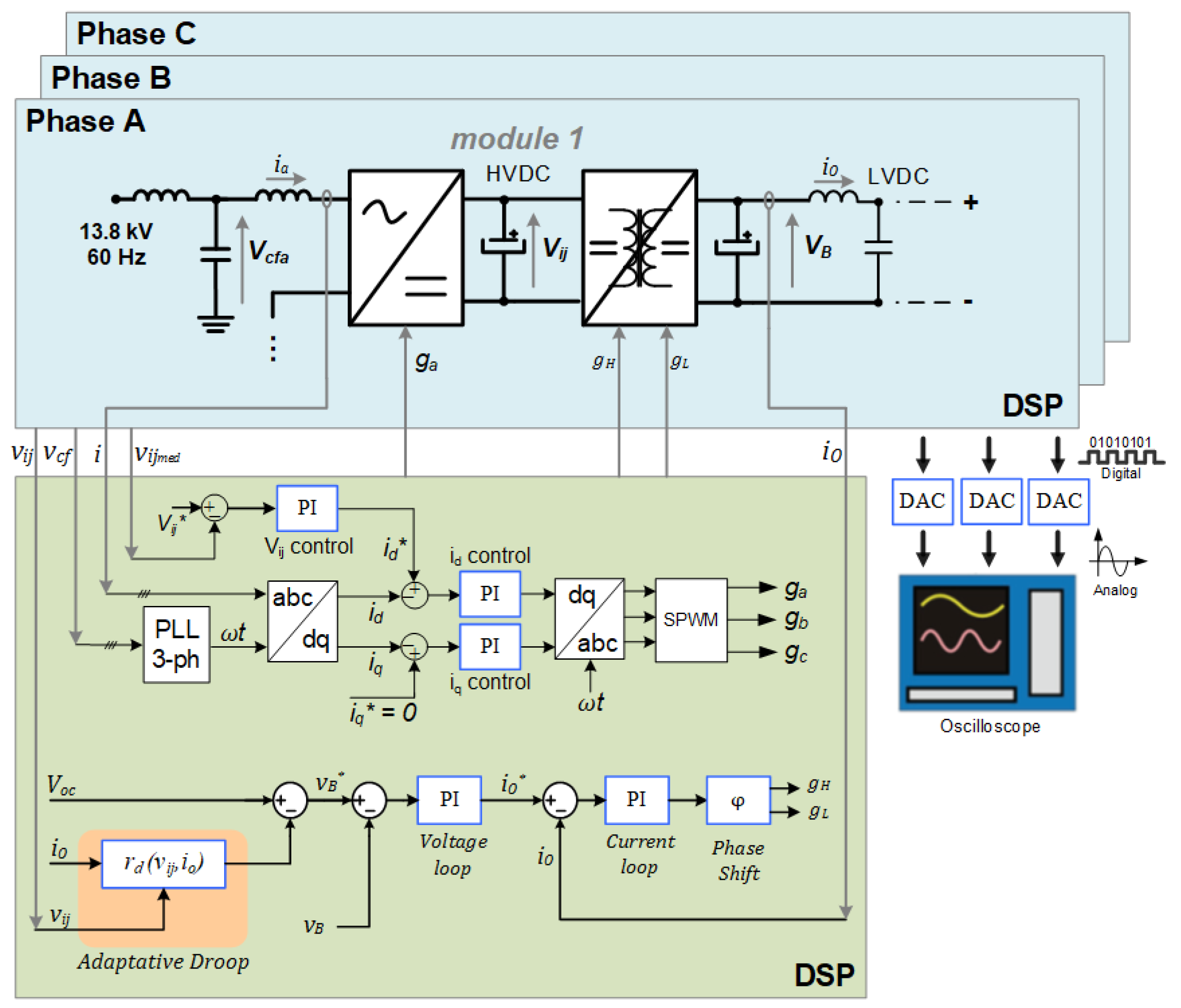
2.1. Three-Phase Modular Cascaded H-Bridge Rectifier
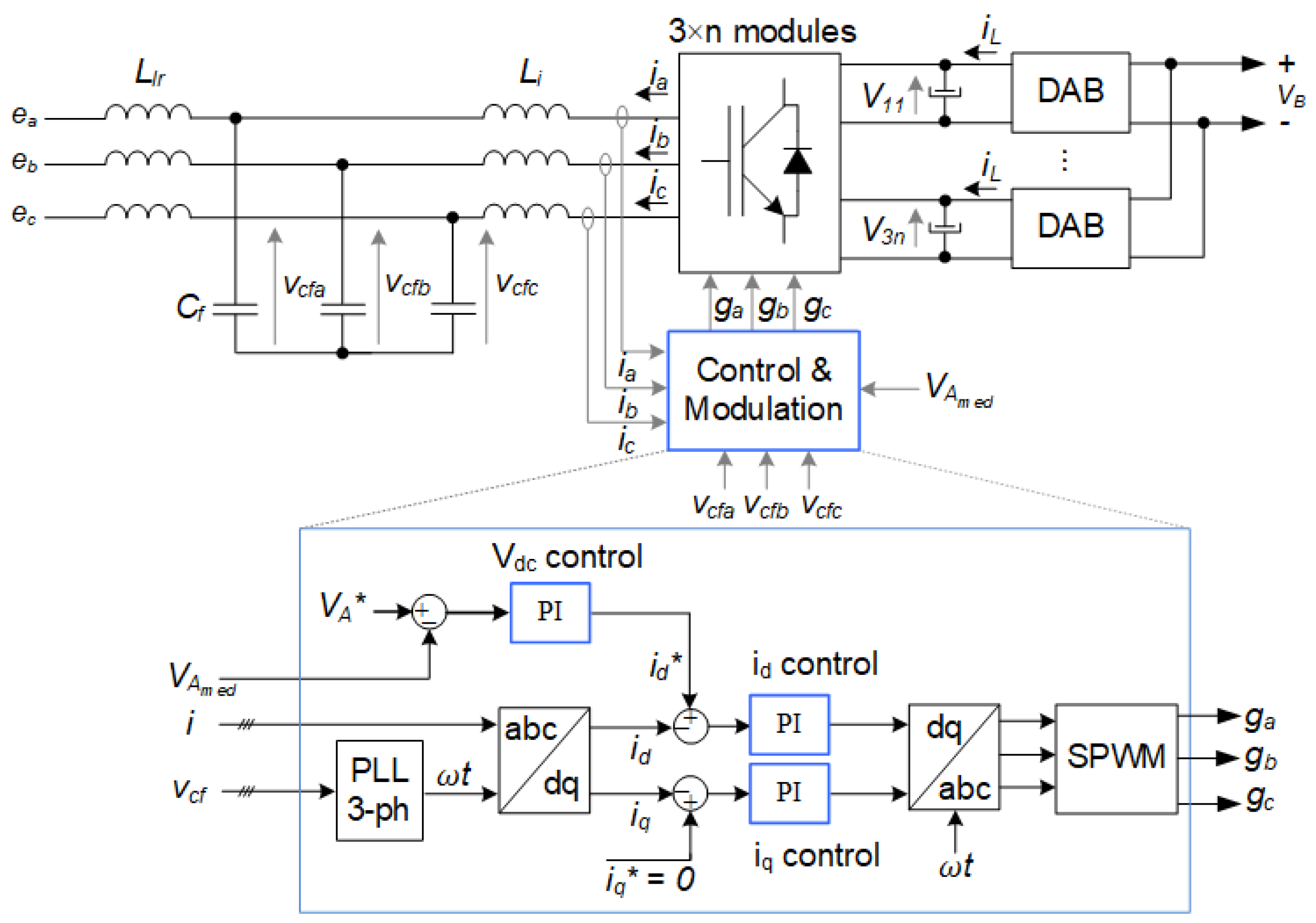
The first stage PWM rectifier is responsible for controlling the voltage of the HVDC link and imposing the HVAC grid currents with low harmonic content and ensuring unit power factor. A three-phase LCL filter interconnects the rectifier stage to the utility medium voltage distribution network and is responsible for attenuating current switching frequency components. The rectifier is implemented by a cascaded H-bridge (CHB) topology, which generates multiple floating HVDC links, and each H-bridge module is operated with a phase-shift carrier PWM modulation. Therefore, the phase voltage at the rectifier output will exhibit a multilevel waveform, for which the number of levels is dependent on the number of modules per phase. This increases the equivalent switching frequency perceived by the LCL filter lowering the requirements on its reactive elements.
The rectifier control is performed in a
-frame, where the active (
) and reactive (
) terms of the three-phase input current are separately controlled. The control diagram of this converter is shown in
Figure 3. The control system receives the HVAC phase currents and voltages and the average of all the multiple HVDC link voltages, which is computed according to Equation (
1), where
n is the number of modules per phase and
is the HVDC link voltage of the
j-th module in the
i-th phase. An external voltage control loop regulates the average HVDC voltage to a reference (
) through a PI compensator. In addition to the voltage regulation, this control loop also allows rejection of load transients. The voltage loop output produces the
d-axis component (
) reference to the LCL filter inductor current control loop. The
q-axis component is forced to zero, in order to ensure zero phase lag between the HVAC grid current and voltage, and, consequently, to guarantee unit power factor. Controller gain adjustments are performed by the pole allocation method [
26]. The selection of those gains must be made to meet response time and disturbance rejection requirements. The strategy adopted to evaluate the performance of control loop responses in terms of those requirements is based on the dynamic stiffness characteristic, which is detailed in [
1,
27].
2.2. Isolated Bidirectional DC-DC Converter
The DC-DC converter is the intermediate stage of the adopted topology, which effectively promotes the reduction of the SST weight and volume. In addition, it provides voltage transformation and galvanic isolation between the medium and low voltage sides. In order to meet the demands of the future smart grid, it must display bidirectional power flow capability enabling the SST to router energy between the utility distribution and the microgrid [
6,
8]. The implemented topology is shown in
Figure 2, and relies on a Dual Active Bridge (DAB) converter that consists of two H-bridges powered by DC buses and connected by a high-frequency transformer. In each module, the high voltage side of the DAB is connected to the CHB HVDC link and the low voltage side of all DAB are parallel together at the LVDC bus. Each H-bridge is controlled in order to impose a two-level square waveform with 50% duty cycle at the transformer terminals. The power that flows through the converter can be controlled by defining the phase displacement (
) between the high (
) and low (
) voltage waveforms [
28]. The relationship between transferred power and H-bridge phase displacement is defined by the transformer leakage inductance; however, depending on the converter power ratings, it would be necessary to add an auxiliary inductance (
) in series with the transformer in order to attain better power transfer control.
Since the rectifier control ignores module mismatches, the input power will be equally distributed to all modules, which as aforementioned can lead to voltage and power imbalance. In order to promote voltage and power equalization, the DAB converters can be controlled individually to extract/inject power from/to their own HVDC links in a way that will compensate eventual module inequalities. Therefore, the control scheme of the DAB plays a significant role in the proposed balancing strategy and it will be described in the following section.
3. Voltage and Power Balancing Strategy
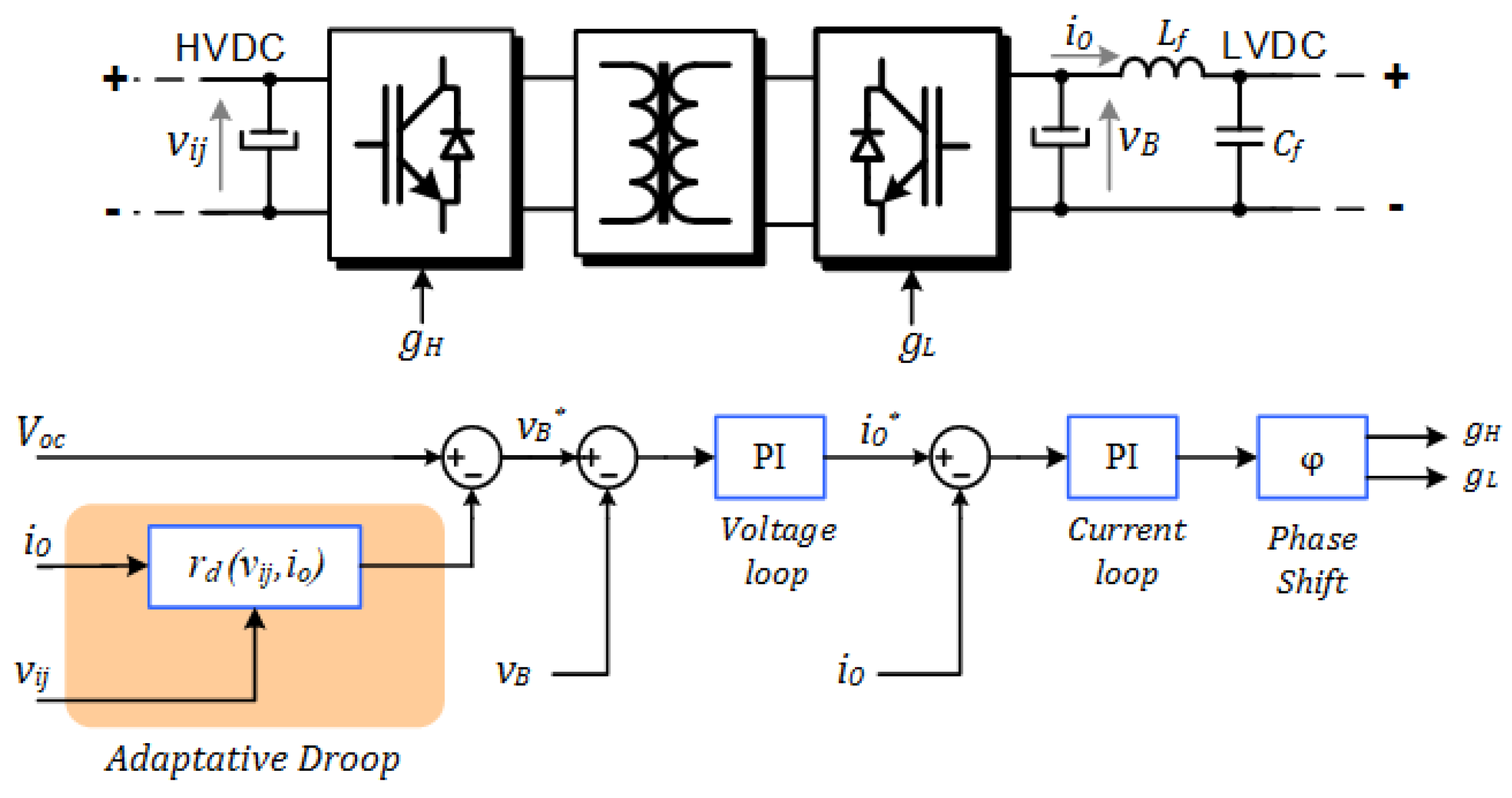
In this section, the proposed control strategy of the isolated DC/DC stage of the power modules will be presented and the mechanisms that enable decentralized HVDC link voltage and power balance among modules will be described. The discussions will be based on the DAB control diagram presented in
Figure 4.
The DAB control strategy presents two cascaded loops, where the outer loop intends to operate the converter, in terms of the LVDC bus perspective, as a droop controlled voltage source, with a voltage reference (
) defined as:
where
is the open-circuit voltage,
is the droop virtual resistance and
is the DAB LVDC output current. A PI compensator establishes the DAB output current reference required for the voltage droop to be attained and an inner control loop with another PI compensator imposes the reference current at the DAB output by altering the phase displacement between the command signals
and
. It is also important to mention that the
filter placed at the converter LVDC output is required to avoid the exchange of switching frequency current ripple among the paralleled DAB.
The droop control enables a proper power sharing among modules at the expense of a load dependent LVDC voltage. As previously discussed, as the front-end rectifier control does not consider eventual differences among modules, employing a control system at the second stage which aims only at power sharing can produce unbalanced HVDC link voltages. In order to solve that issue, it is proposed that the droop virtual resistance should be a function of the instantaneous HVDC voltage and power flow of the module, the latter defined by the LVDC output current direction, i.e., the droop resistance value should be autonomously adapted according to the HVDC link voltage level, hence:
where
is a fixed pre-defined resistance used in all modules and
is a droop virtual resistance function, defined as:
where
is the average HVDC voltage reference and
p is a parameter that affects the intensity with which the resistance will be modified in relation to the voltage deviation. Therefore, whether a module HVDC link voltage differs from the reference, its droop resistance will be modified forcing an instantaneous power imbalance between that module and the rest, in order to promote the gradual reduction of the voltage error. When the module converges to the voltage reference, the adaptive function will converge to 1 and the droop resistance to
, leading to equal power distribution.
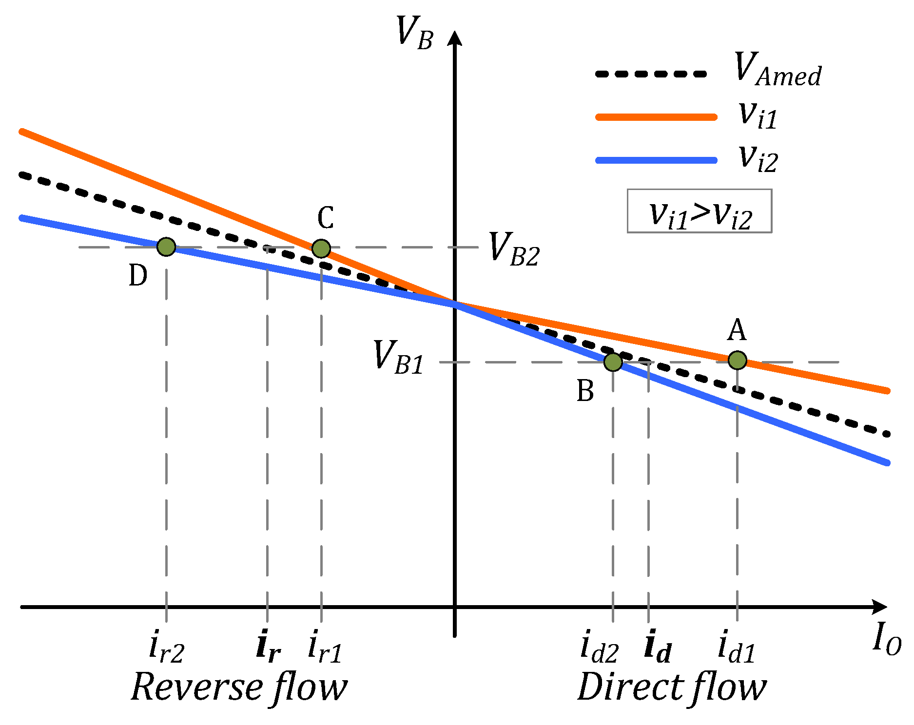
Figure 5 illustrates how the adaptive function affects the static voltage droop curve of two modules with distinct HVDC link voltages.
In this example, the droop adaptive function is applied to two converters, where converter 1 has an instantaneous HVDC voltage () higher than the reference () and converter 2 presents a lower voltage (). In this condition, if the SST is injecting power into the LVDC bus (direct flow), the droop resistance of converter 1 will be lowered in relation to , whereas the resistance of converter 2 will be increased. The LVDC bus voltage will reach an equilibrium point ; however, due to the adaptive function influence, the operating point of the converters are different, point A for converter 1 and point B for converter 2, which indicates that the total current will be unevenly distributed between both converters with converter 1 providing a higher output current than converter 2. Therefore, as converter 1 output power will be higher than the system average power, its HVDC link voltage will be decreased, whereas converter 2 HVDC voltage will be increased. In the case of a power flow reversion, the voltage equalization logic is inverted, and a new equilibrium () will be achieved, with operating point C for converter 1 and D for converter 2. In the new condition, converter 1 will absorb less power from the LVDC bus than converter 2, which also will decrease converter 1 voltage and increase converter 2 voltage. In both cases, the voltage errors will gradually be reduced and the HVDC voltages will converge to the reference.
The intensity with which the droop resistance will be altered in terms of a module instantaneous HVDC voltage is regulated by the parameter p; a higher p will promote a greater power imbalance and, a priori, a faster reduction of the voltage error. It is important to mention that, if the constructive differences between modules induce significant efficiency inequality, a perfect balancing of the HVDC links voltage will require the existence of a power imbalance among the modules, i.e., in this scenario, the proposed strategy will not be able to ensure concomitant voltage and power balance; however, the algorithm will seek an equilibrium point that minimizes both voltage and power errors.
Assessment of the Adaptive Droop Function Behavior
In this section, the behavior of the proposed adaptive droop function in terms of voltage balancing capability and the influence that the SST control parameters have on it will be discussed. In order to perform the studies needed to characterize the voltage balancing performance, a simulation model was elaborated in MATLAB/Simulink based on the average model of the converters employed in the SST architecture. The utilization of an average model allows for capturing information concerning the dynamics of very complex structures with faster simulation times, enabling extensive parametric variation studies to be carried out in a very practical fashion; therefore, such a method was employed in the design and control tuning of the SST.
The analyses presented in this section and afterwards are based on an 100 kVA SST connected to a 13.8 kV/60 Hz three-phase distribution grid at the HVAC side and to a 380 V LVDC bus. The system is designed assuming the use of 6.5 kV IGBT power devices, hence each phase of the SST is composed of six series cascaded modules of 5.6 kVA with an HVDC link of 2.087 kV each. The design of the converter components and controller gains employed techniques already consolidated in the literature; therefore, it will not be detailed in this paper.
Table 1 presents the parameters considered for the SST.
Since parameter mismatches between modules, e.g., components tolerance, unequal loss distribution, etc., can have a significant impact over voltage and power imbalance, this condition was included in the simulation model. It was assumed that reactive elements and the DAB transformer turn ratio are susceptible to a ±20% tolerance, thus a random function with a normal distribution was applied to individualize the values of the reactive elements of each power module. Moreover, another random function with uniform distribution was used to define the efficiency of each module ranging from 90% to 95%, in order to incorporate power loss difference among them. The initial conditions of each module HVDC link voltage were also randomly chosen in a ±20% range around the reference value. Although the proposed strategy will not allow for such high voltage deviation, as will be later shown, those initial values were chosen in order to better evaluate the evolution of the HVDC voltage error over time.
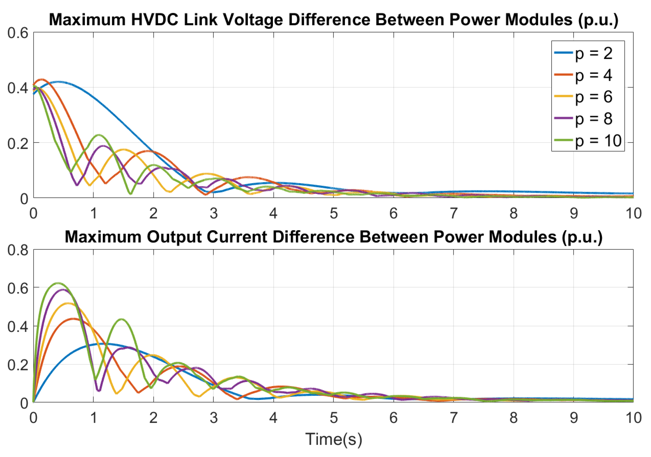
Figure 6 presents the voltage error time response of a SST with a 50 kW (0.5 pu) load for a set of
p-values. The maximum HVDC voltage difference between two modules in the same phase are shown along with the maximum LVDC output current difference for those same modules. The values are normalized by the HVDC link voltage reference and the LVDC nominal output current for each module, respectively.
Figure 6 shows that independently of the value selected for
p, the voltage difference will be reduced to very low levels. It is important to mention that the HVDC voltage trajectory for each one of the modules has an under-damped behavior; therefore, since the data presented in the figures of this section describe the maximum difference between modules, the voltage and output current oscillations will define the bumps observed in them. It can be noticed that an increase in
p will provide an increase in the frequency of voltage error oscillations, which at the first moment will be translated into a faster voltage difference reduction and consequently a higher current imbalance. However, the parameter increase does not seem to have a significant impact on the system time constant, since the setting time is approximately the same and, for
, the response envelopes are very similar. Another important result is that the system presents a steady state voltage error, which is 0.016 pu for
, 0.007 pu for
and 0.0025 for
, which shows that increasing
p will lead to a lower voltage error. The same situation is observed regarding the current error, which is 0.017 pu for
and 0.008 for
. Nevertheless, as the voltage equalization dynamic response does not show great improvements with higher
p-values, and, for
, the voltage and current error are already below 1%, the selection of high values of
p is not mandatory; therefore, for the remainder of this paper,
was considered.
Subsequently, the impact of the SST control loops over the voltage balancing strategy was assessed; however, no substantial influence of the rectifier control and the DAB inner current control loop have been observed. The DAB voltage control loop, on the other hand, have shown to be relevant to the proposed strategy performance.
Figure 7 and
Figure 8 present the voltage and current maximum differences evolution for a set of
and
values, respectively. In both cases, the SST load was kept in 50 kW. It can be observed that the proportional gain has no significant influence on the response; the integral gain, however, has an important impact on it. It is noticeable that the integral gain mainly defines the response damping factor, which can be increased with higher values of
. It indicates that a special attention must be given to the DAB voltage loop design since low integral gain values can lead to poorly damped systems and compromise stability.
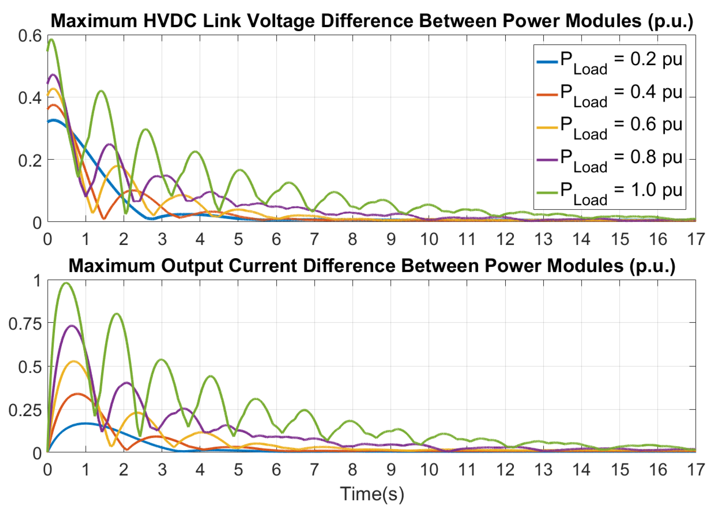
Figure 9 presents the system behavior for different load values. It can be seen that the load influences the response time constant, increasing the oscillation frequency and lowering the damping factor with the load increase. Although the result suggests that the control design should be performed considering the converter near its nominal power,
Figure 9 does not indicate that load variation will drive the designed SST into instability or hampers voltage equalization.
4. Hardware in the Loop Simulation
In this section, the procedures for high level programming with MALAB/DSP integration are presented to validate the control laws implemented in the modular topology used for the SST design. In this way, the microcontroller’s programming has a different approach from the conventional one, since there is no need in developing code lines. Taking into account that many control loops require validation, the methodology used in this work assists in performing the tests, collecting the results and evaluating the operation of the system without the need to build the physical circuit, which minimizes costs and reduces time of project development [
29].
Therefore, the Hardware-In-the-Loop (HIL) method is a simulation technique that encompasses both virtual elements and real elements. Currently, this technique has been widely used to test embedded control systems, where both hardware and system software are validated [
30].
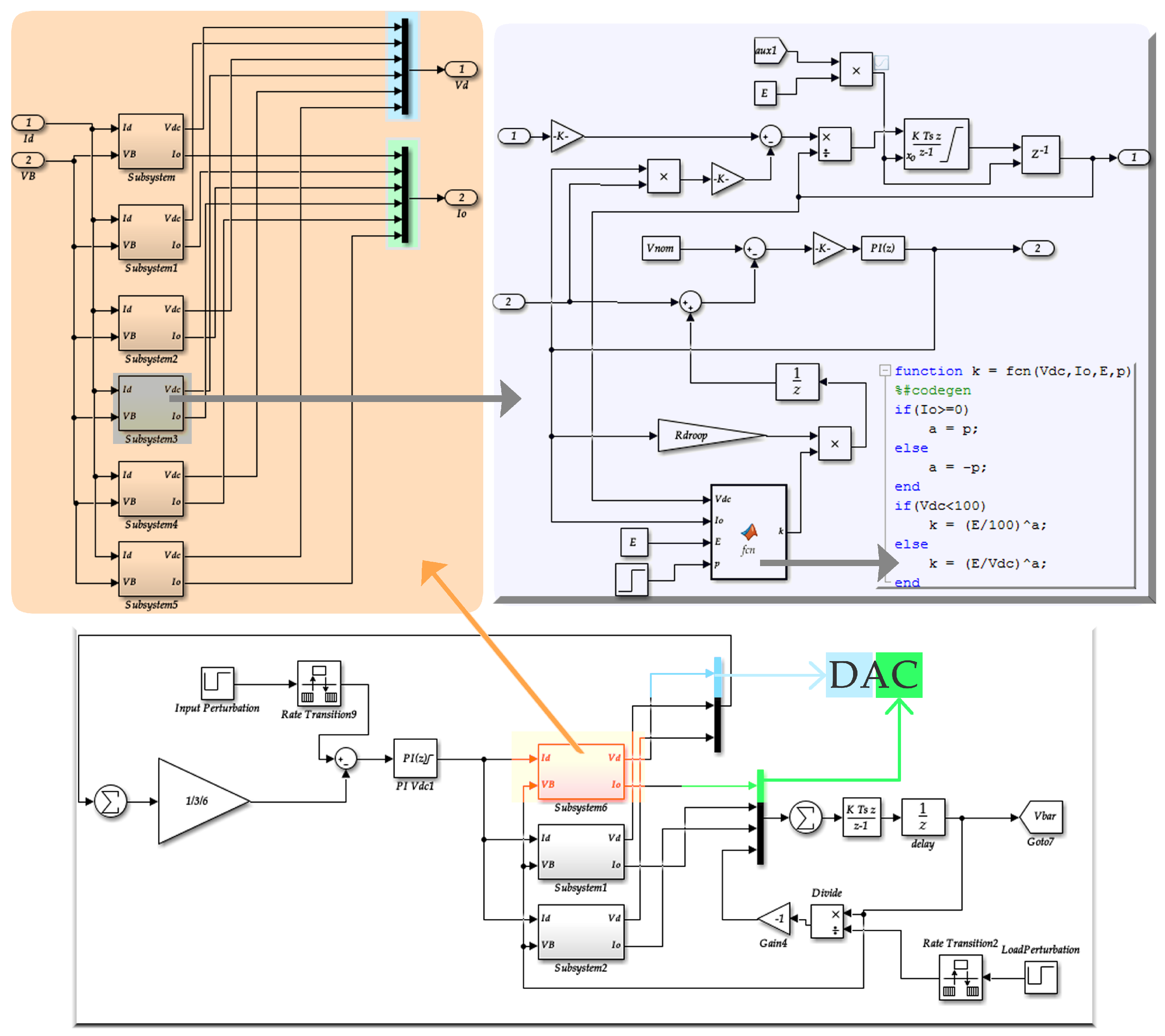
Figure 10 illustrates how the SST modules and control algorithms are implemented and embedded in the DSP. For simulation of SST with HIL, it is necessary to obtain the mathematical model of the converters that represents the SST module, as well as the equations of the control algorithms [
31].
With this in hand, the model can be constructed using the MATLAB/Simulink software blocks, as shown in
Figure 11. This figure includes a flowchart which shows the MATLAB/DSP integration through codes are embedded, which presents the details of the mathematical model of the converters and the control algorithm. After this implementation and the validation of the model, the system is embedded in the DSP. When using Simulink’s external mode and a proper compiler for the DSP, the model will be automatically converted into code lines and then embedded into the target. Thus, the target will execute the code emulating the converters and the control techniques. The DAC blocks available in the C2000 Texas Instruments package (Texas Instruments, Inc, Dallas, TX, USA) [
32] of Simulink permits the visualization of the signals in the correspondent pins of the DSP. In this way, the external signals can be displayed on an oscilloscope, as shown in
Figure 10.
Thereby, it is possible to verify the performance of the control strategy in equalizing the voltages of the SST HVDC buses and promoting power sharing. Besides the independence of the physical prototype, the methodology in question has other advantages [
23,
33]:
There is no need for costly Real-Time Simulators (RTS) systems, such as those offered by OPAL RT, Typhon HIL, dSPACE and RTDS. In the same sense, it is possible to use the method remotely, in residences, in the laboratory, on PCs and on laptops, without being conditioned to a complex system—which involves both hardware and software previously installed;
It is possible to emulate only the SST model and perform several tests that don’t necessarily involve a control law;
The system control is embedded and its proper functioning can be evaluated in the DSP, thus facilitating the determination of the processing times of each step of the algorithm. It is possible to monitor, make initial parameter updates, controller gains, input and load disturbances, etc., all in a didactic way through the interface offered by MATLAB/Simulink.
In addition, there is the possibility that the code is to emulate the model or the control system independently of a PC/laptop. To do so, simply loaded into a flash memory of the embedded system (tests are limited to DSP input/output capabilities, for example, DAC (Dual Active Bridge) and other digital/analog ports).
In order for the simulator to operate in real-time, and so, to show the appropriate results, the tool will be used in a Real-Time Workshop [
34]. In this way, the generated models in MATLAB/Simulink software will be executed in real-time. Thus, it is verified if the hardware is able to perform all its tasks in a predetermined time loop and synchronized with the rest of the system. This methodology has already been validated in 2nd order [
30,
35] and in 4th order [
23] converters, which have simple implementation topologies. The great challenge of this work is to extend this approach to a more complex case study, which was only possible with the evolution of the current embedded systems.
5. Software Simulation and HIL Experimental Results
In this section, the dynamic behavior of the voltage and power balancing strategy will be evaluated considering operating point perturbations such as load steps and power flow reversions. The analyses presented in the section were also performed by MATLAB/Simulink simulation, considering a complete switched model of the SST. The experimental results obtained from the HIL are also presented in order to prove that the embedded system of the DSP shows similar results to those of the designed and simulated converters. The system parameters are the same considered in
Section 3 and described in
Table 1. The droop adaptive function employs
and the reactive elements of each power module were also individualized using random functions as previously described. For all simulations, the initial conditions for each module HVDC voltage and the SST load power are the same.
5.1. Software Simulation Results
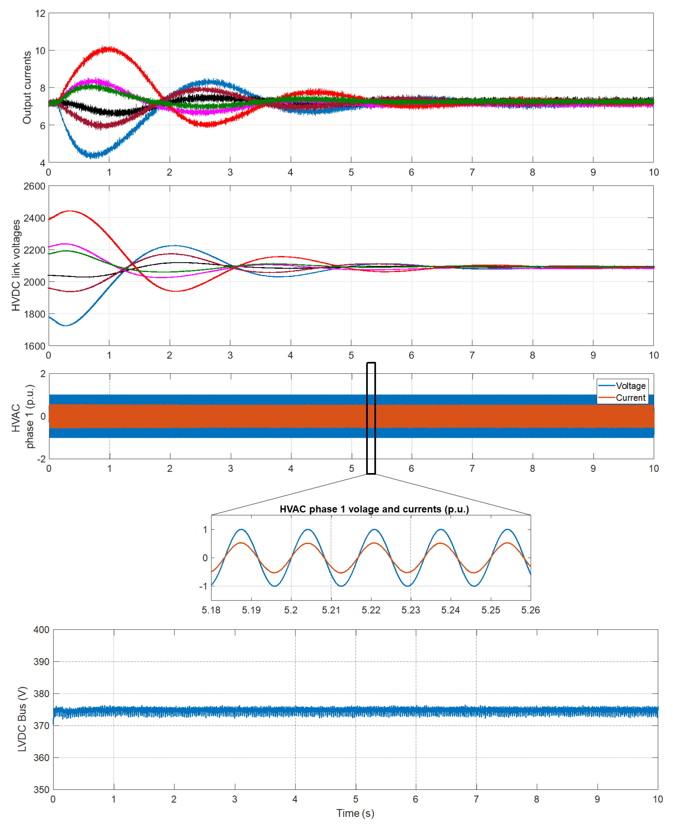
Figure 12 presents the simulation results for the SST with a 50 kW (0.5 pu) load. The DAB droop adaptive function is enabled shortly after the beginning of the simulation. At
s, the maximum voltage difference between two modules in the same phase is 605 V (0.289 pu) and exhibits a divergent tendency due to mismatches in the power modules. After the droop adaptive function is initiated, the DAB output currents are unbalanced leading to a change in the trajectory of HVDC voltages. The voltage difference reaches a maximum of 716 V (0.343 pu) at
s and is gradually reduced afterwards, converging in
s, where the voltage difference between modules is 16 V (0.0077 pu). The maximum output current difference observed is 5.5 A (0.368 pu) in
s.
It is noteworthy that, during the equalization period, the DAB behavior has not produced any significant impact over the active rectifier response, since both HVAC phase voltages and currents presented no alterations during the simulated period (the HVAC voltage is normalized by 11.268 kV and the current, by 5.92 A). The phase currents are balanced and present a 0.5 pu amplitude with unity power factor. This behavior was already expected, since the rectifier actuates on the average of the HVDC link voltages, thus internal voltage inequalities are mostly irrelevant to the front-end stage control. The LVDC bus voltage is also constant during the simulated period, but a small disturbance occurred at the adaptive function initialization. The small disturbance is due to the sudden variation of the DAB droop resistances; however, as the average of all HVDC voltages is regulated by the rectifier, the equivalent droop resistance seen by the LVDC bus will not diverge from the pre-equalization value. The results show that, even though the voltage equalization function does promote DAB output power oscillations, SST input and output power will be constant during the equalization process.
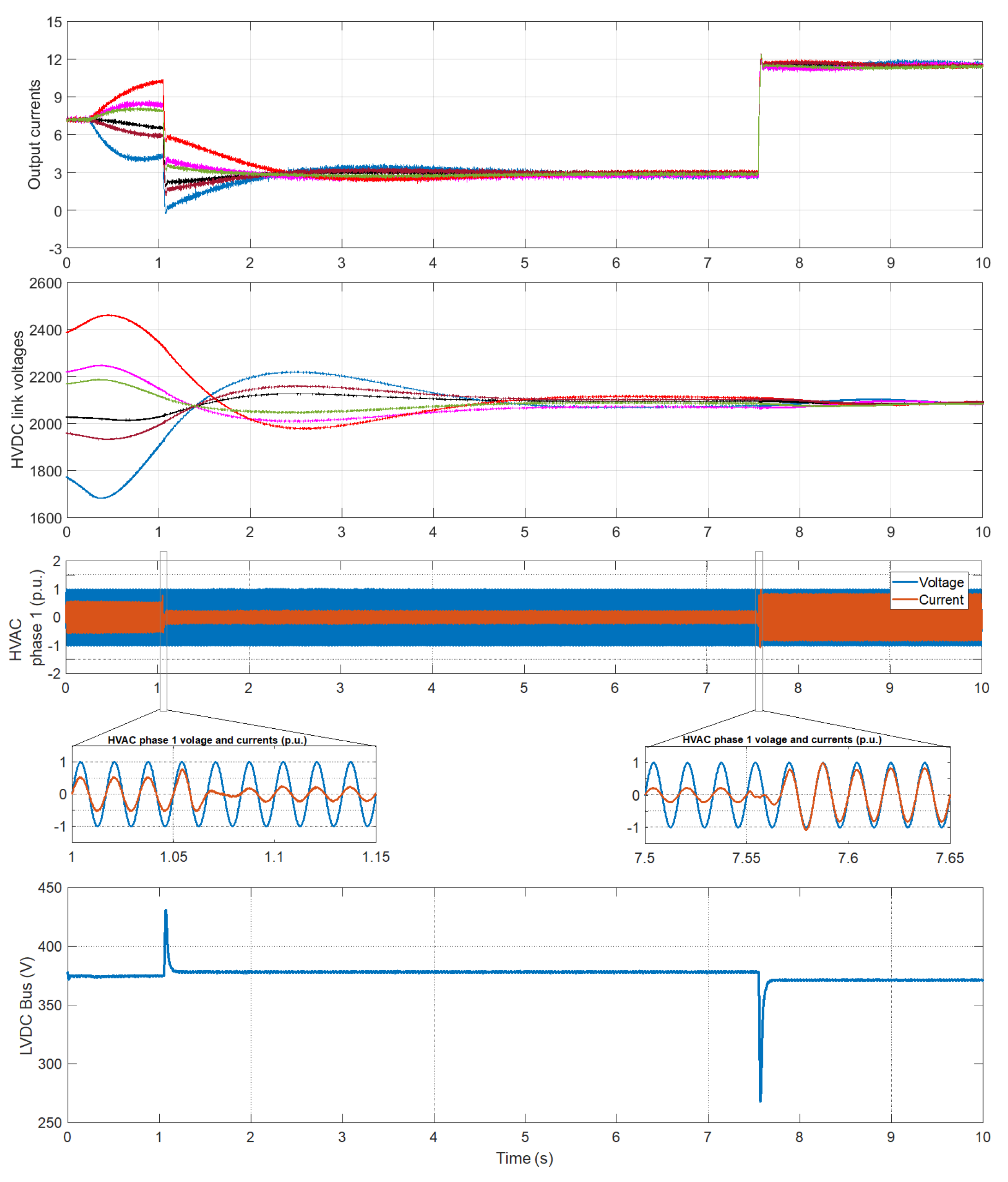
Figure 13 presents the simulation results for the SST submitted to load steps. At
s, the LVDC load is reduced 0.3 pu, from 50 kW to 20 kW and in
s the load is increased 0.6 pu, to 80 kW. It can be seen that the load variation alters the equalization time constant, e.g., the voltage oscillation frequency is reduced with the load reduction to 0.2 pu and also settles earlier than the 0.5 pu situation, in
s. However, the voltage imbalance observed in this condition is higher, 42 V (0.02 pu). When the load is stepped-up, the system seeks to reduce that error, initiating a new equalization process, therefore the DAB output currents are disturbed once again, with lower amplitudes obviously, but with a higher oscillation frequency. Such behavior complies with the predictions provided by the studies present in
Section 3. During the entire equalization process, the HVAC voltages and currents, as well as the LVDC bus voltage, were not affected, they only responded to the load variations and not to the HVDC voltage and DAB current oscillations.
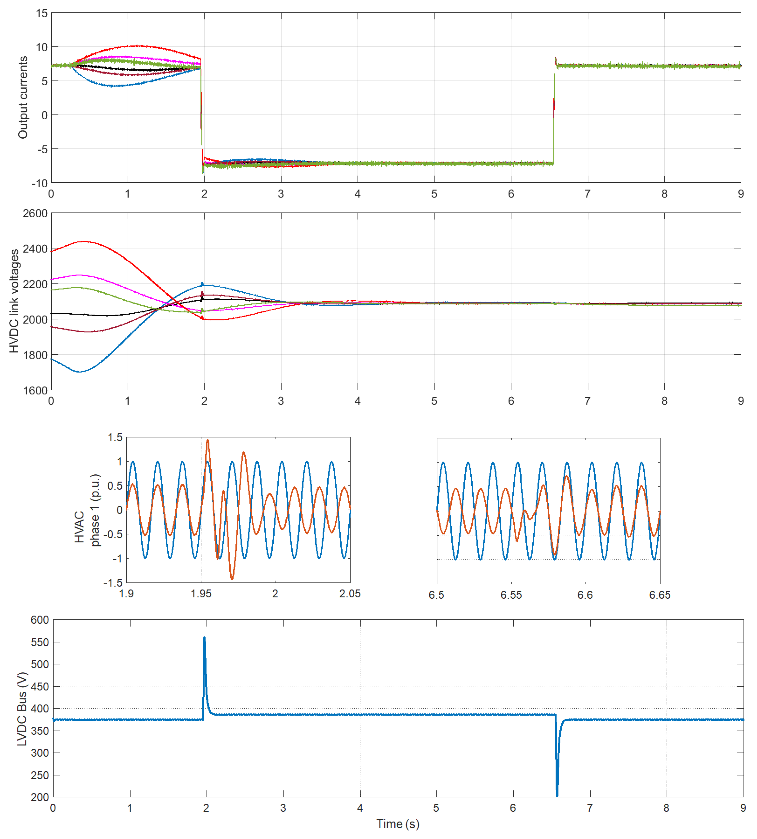
Figure 14 presents the simulation results for a full power flow reversion of the SST, which occurs in
s and
s. It can be noticed that, although the power managed by the SST in both directions is exactly the same, when the flux is reversed, the time constant is decreased, leading to a faster equalization, which occurred in
s with a voltage imbalance of 9 V (0.0043 pu). Moreover, once the voltage is balanced, the second power flow reversion does not induce further voltage deviations, which suggests that, after the droop adaptive function attained voltage balancing, shifts in the operating point of the SST will not cause the HVDC link of the power modules to diverge. The equalization process once again has shown no impact over the variables of the HVAC and LVDC buses.
5.2. HIL Experimental Results
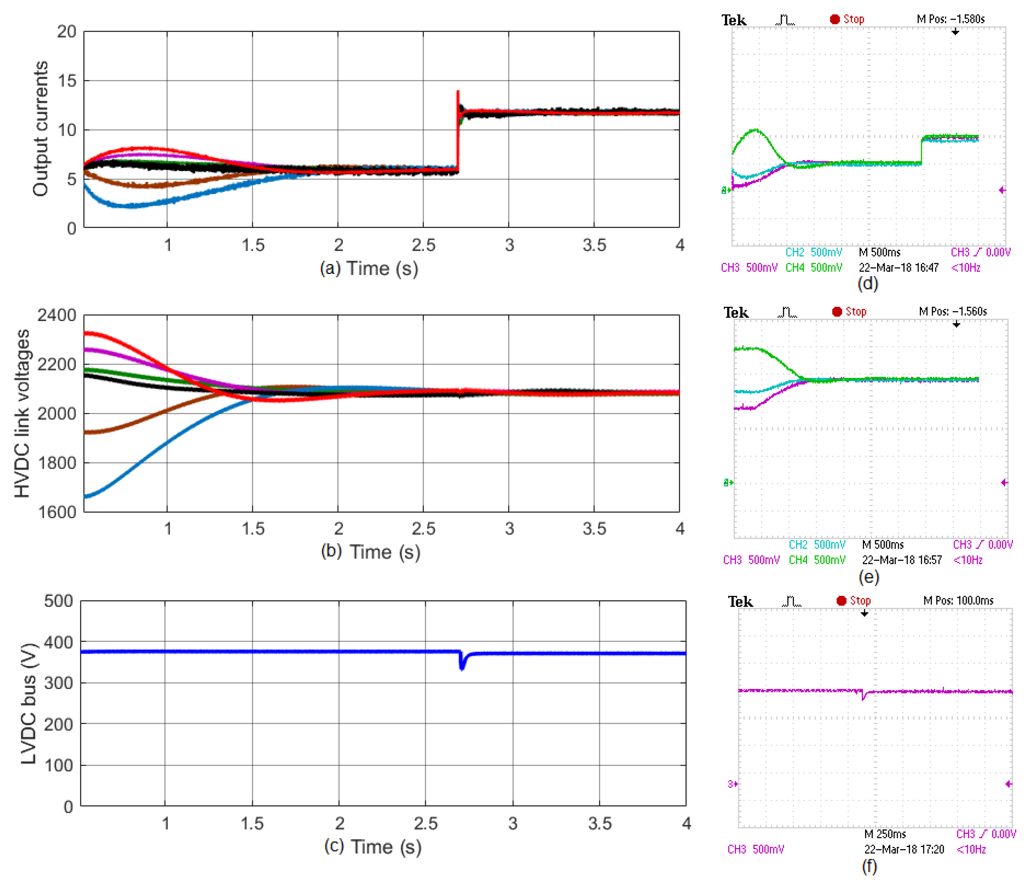
Figure 15 shows the simulation results in MATLAB and real-time simulation for the SST with a charge of 80 kW (0.8 pu). To facilitate comparison, the simulation results are presented on the left side and HIL results on the right side. In addition, the variables presented in the oscilloscope are normalized and included in the range of the DAC converter of the DSP (0–3.3 V, resolution 12 bits). The results show that with the performance of the adaptive droop function, initially the DAB output current are unbalanced causing a change in the trajectory of the HVDC voltages, which gradually converges to the reference value, which occurs at
s. From this point, all modules have almost the same HVDC voltage value and provide the same power.
Figure 15c,d show the signals of the currents and voltages obtained on the oscilloscope. Due to the number of DACs available on the DSP and channels on the oscilloscope used for measurement, only the voltage/current signals of three modules are displayed. These results show that the embedded model in the microcontroller behaves similarly to the simulated results in MATLAB. It is observed that in a short time period there voltage and power balance between modules is achieved.
Figure 16 presents the results for SST when submitted to the load step. At the beginning, the SST is exposed to a load of 0.4 pu and after the equalization of the voltage and current, there is a variation of the load to 0.9 pu (at time
s). As seen by the voltage curves, the load disturbance is insignificant, not affecting the balancing between the modules. In the LVDC bus,
Figure 16c, a slight momentary voltage sag is observed at the instant of load increase, being quickly regulated by the control loops of the converters. A similar behavior is observed in the HIL experimental results, as shown in the graphs of
Figure 16d–f.
Figure 17a shows the simulation result for a power flow reversions of the SST. At the beginning of the simulation, the microgrid connected to the LVDC bus is consuming a power of 1 pu (100 kVA) of the medium voltage network (HVAC). At the moment of
s, in which the power and voltage balance between the modules has been already attained, the flow reversion occurs, produced, for example, by a distributed generation source present in the microgrid, causing this energy to be injected into the grid. As noted by the simulation charts, the reversion also has an irrelevant impact on the balance between the modules. The LVDC bus presents a slight increase in voltage but is quickly corrected by the control techniques. The current and voltage of phase 1 of the medium voltage network (HVAC) show that, in both directions of the power flow, the power factor remains unitary and a displacement of 180º between these signals, evidencing the change in the flow direction of power.
Figure 17b shows the HIL experimental results. For the purpose of analysis, only one of the output currents (green curve) of one of the modules and the voltage of the LVDC bus (purple curve) are presented and also only the details of the instant of the power flow reversion are shown. The current signal shows the change of direction (negative signal) and the bus voltage has a small increase at the time of flow reversal.
As observed in all simulations and HIL results, after power and voltage balancing between the SST modules, any disturbance to SST affects in a derisory way the imbalances between them. Thus, the effectiveness of the adaptive droop based control strategy implemented in the DAB control loop.
6. Conclusions
This paper proposed a control strategy for a three-stage cascaded multilevel solid state transformer capable of promoting second stage HVDC link voltage equalization and power sharing among modules in a decentralized fashion, i.e., without the need for information exchange between modules. In this proposal, the Dual Active Bridge converters employed to interface the HVDC and LVDC buses use an adaptive droop control scheme that modifies the virtual droop resistance in function of the module instantaneous HVDC voltage and power flow direction. Therefore, whether any HVDC voltage difference between modules occurs, the droop function will promote a module output power imbalance that will force the voltage error to be gradually reduced over time.
The behavior of the proposed strategy and the influence of control parameters over its performance were assessed through MATLAB/Simulink simulations of an 100 kVA SST with six cascaded modules per phase and real-time simulation application with high level programming. The simulation results have shown that the equalization dynamics is governed by the DAB voltage control loop and that it can promote steady state voltage and current errors below 1% even during load variation and power flow reversion conditions. Moreover, the equalization strategy does not impact the behavior of HVAC currents and the LVDC voltage, i.e., the voltage balancing is performed by means of power distribution adjustment between modules, which is transparent to the elements connected to the SST ports.
The mathematical model of the converters and the control algorithms were elaborated and then embedded a microcontroller. Hence, the experimental results of the proposed system are obtained in real time quickly and inexpensively, and the signals are visualized on an oscilloscope. The results obtained with the HIL setup show great compatibility with those simulated, which clearly demonstrates the effectiveness of the mathematical model obtained from the design of the static converters. In this paper, a platform to test and validate power converter models and control strategies that pose great challenges of physical implementation is presented. This can greatly assist the designer in the phase prior to the experimental setup.

 ,
, 


