Automatic Adaptation of Multi-Loop Wireless Power Transfer to Variable Coupling between Transmit and Receive Coils

Abstract
:1. Introduction
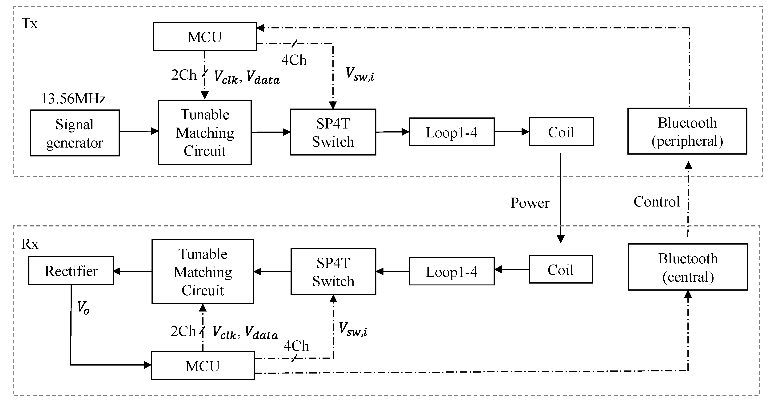
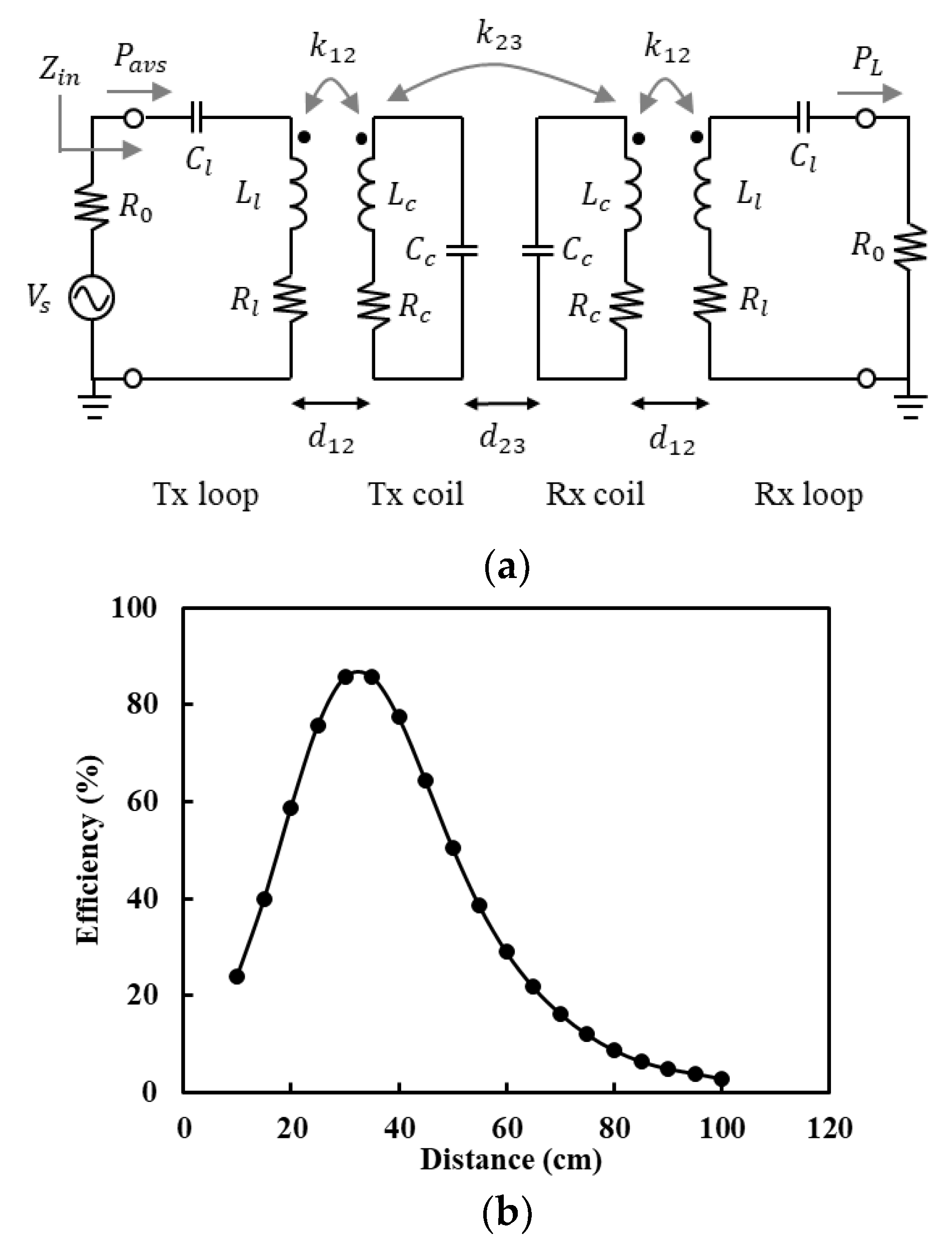
2. Proposed WPT System
2.1. System Operation
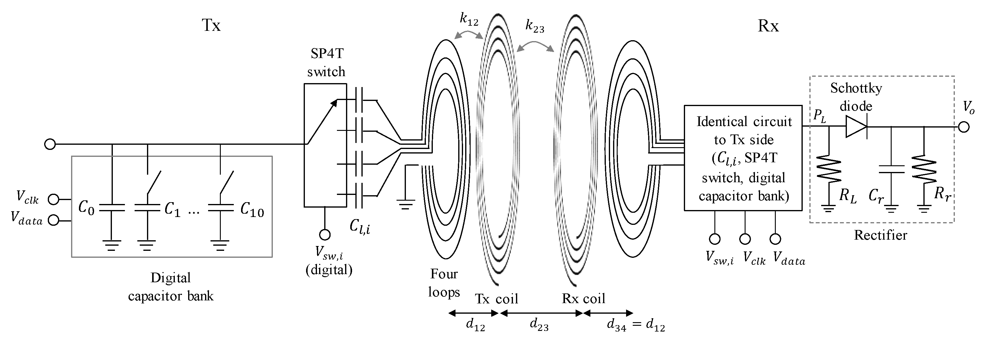
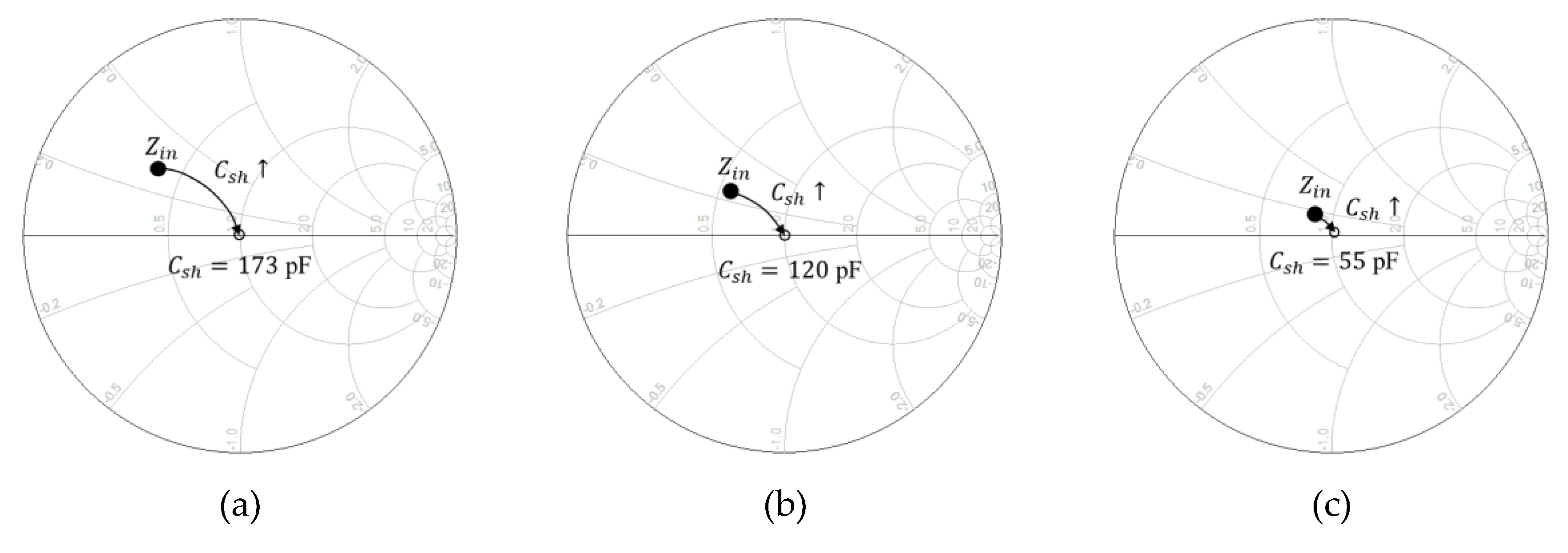
2.2. Tunable Matching Circuit
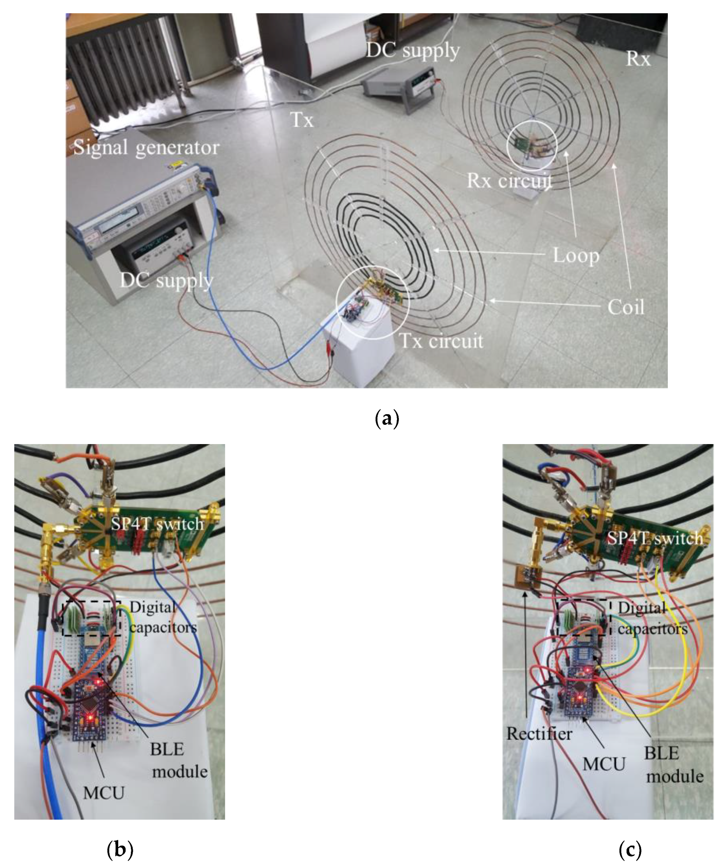
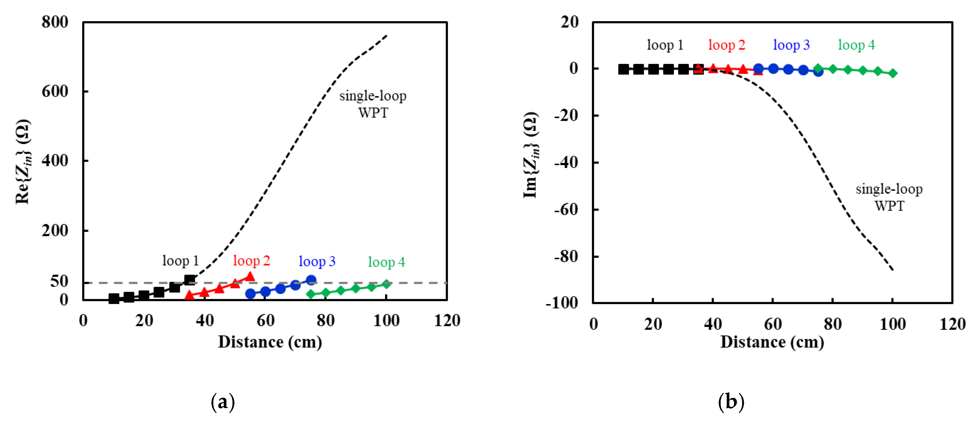
2.3. Coil and Loops
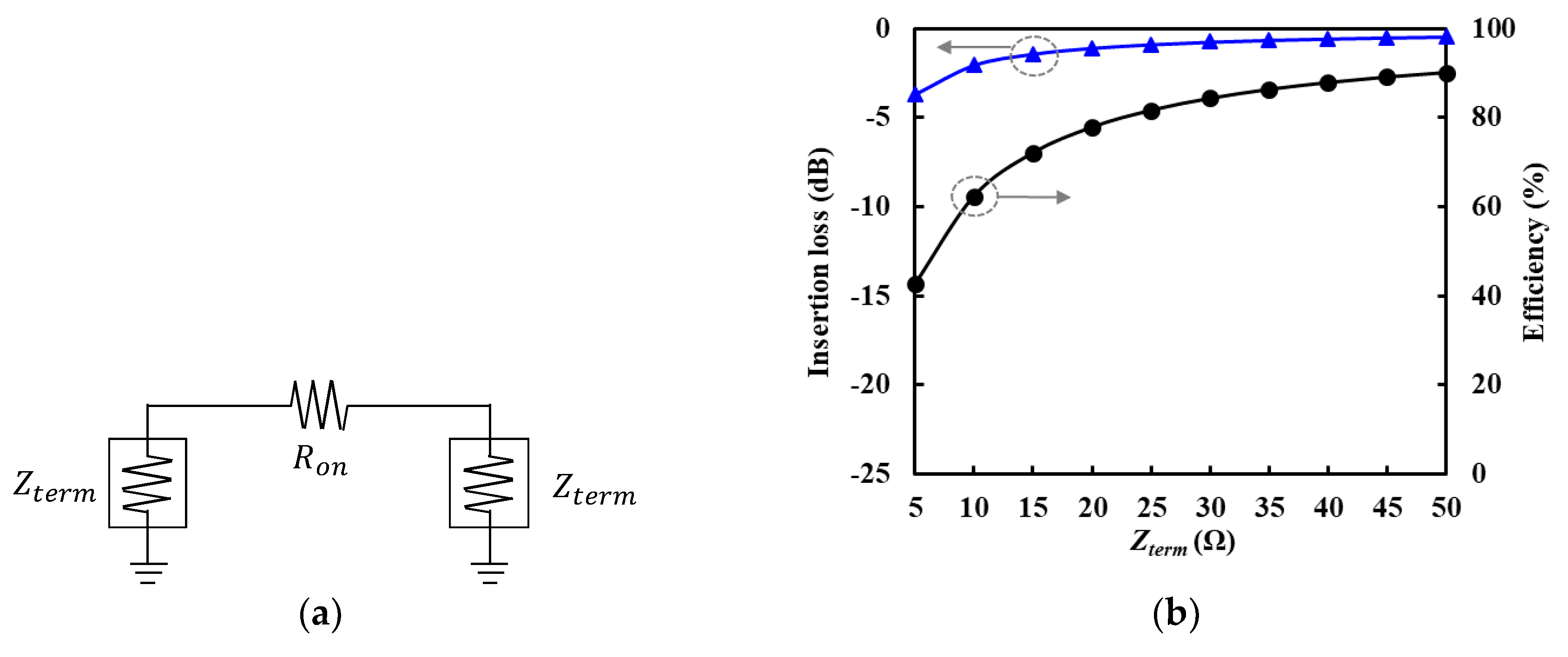
2.4. SP4T Switch
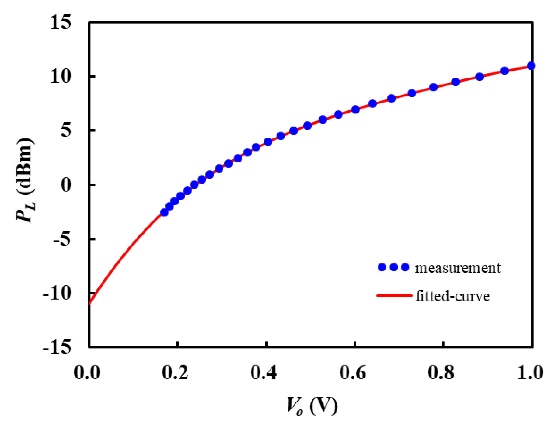
2.5. Rectifier
2.6. MCU and BLE Module
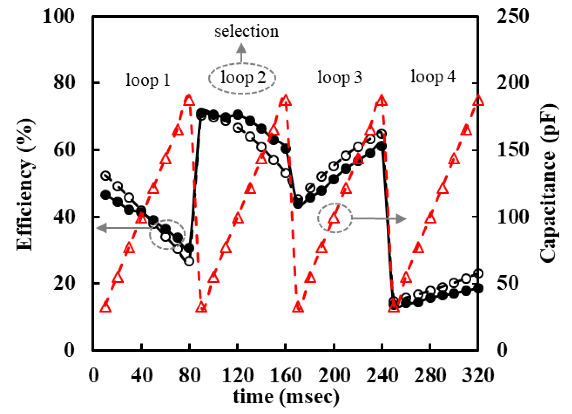
- Both Rx and Tx connect the loop 1 ( = 3.3 V for = 1 and 0 V for otherwise).
- For a selected loop, both Rx and Tx change the capacitance from low to high values at 8 points, and Rx MCU measure the rectified voltage at each capacitance.
- The procedure 2 is repeated for the loop 2, 3, and 4.
- Rx MCU determines the optimum loop and capacitance, providing highest and , and send this information to Tx MCU through BLE.
- Both Rx and Tx set the optimum loop and capacitance determined in the procedure 4.
- Rx MCU measures and calculates periodically (every one second). If is 5% less than , select the loop 1 and repeat the process from the procedure 2.
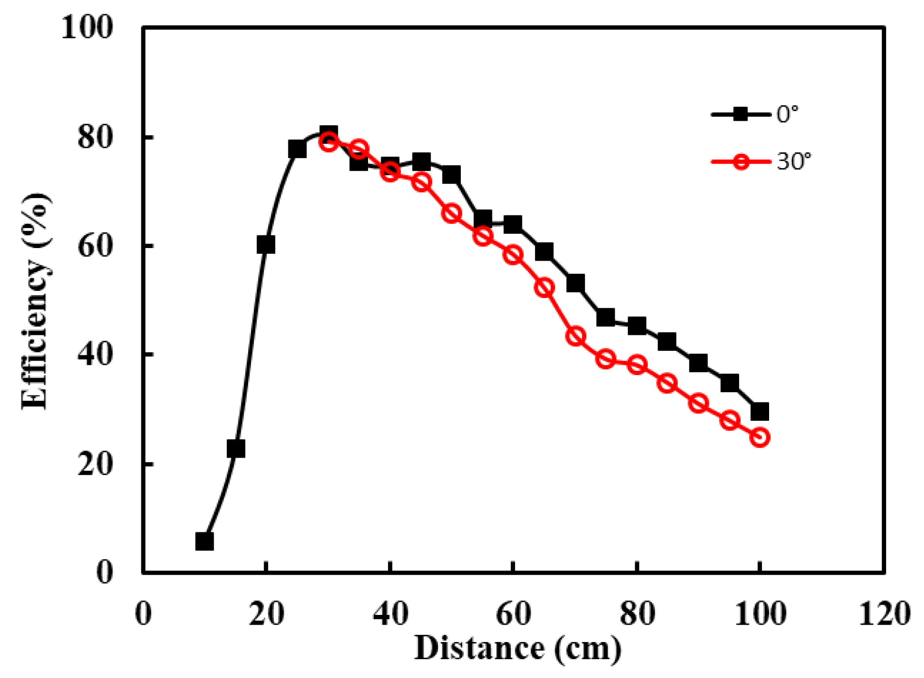
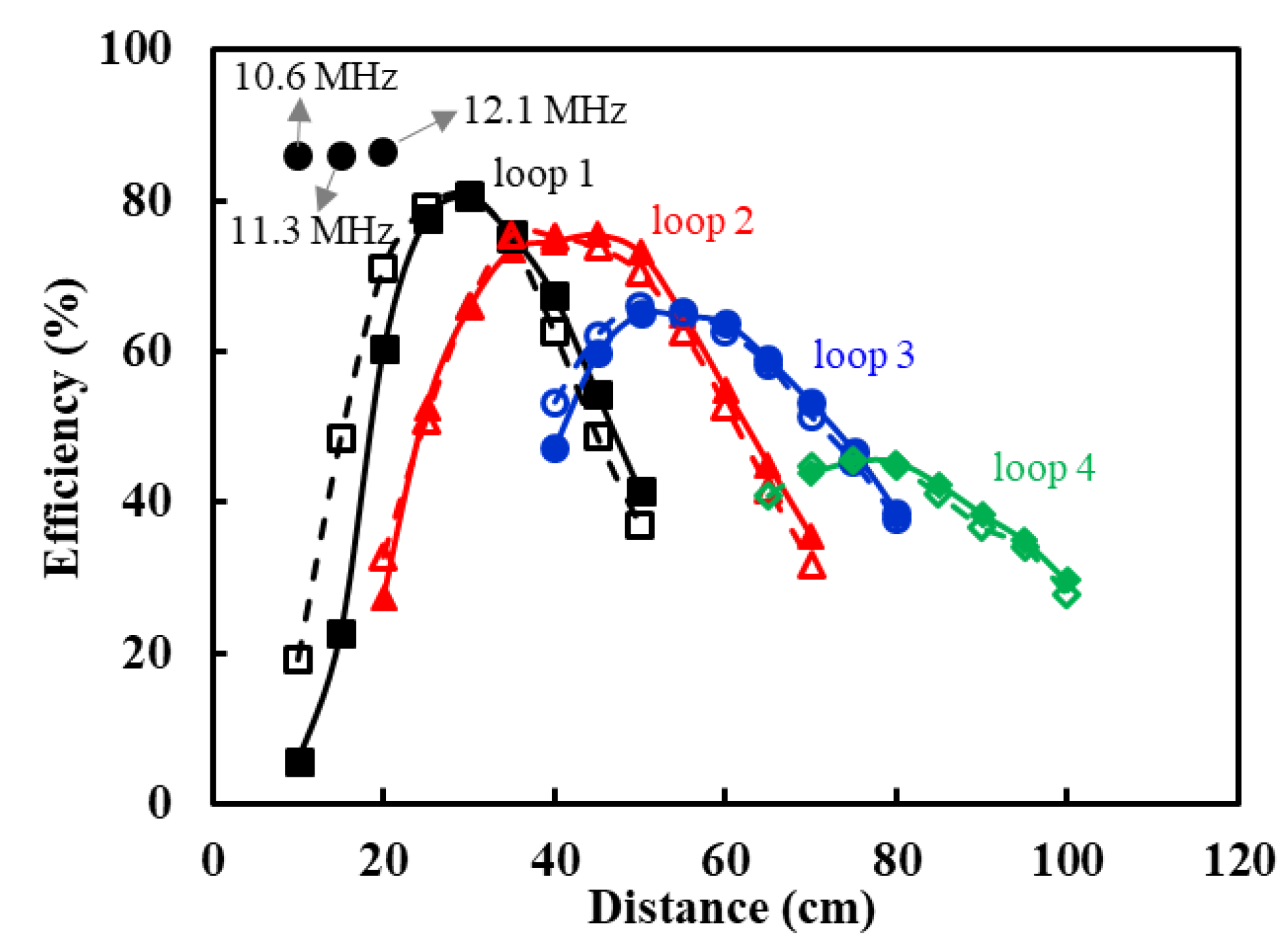
3. Experimental Results
4. Conclusions
Author Contributions
Funding
Acknowledgments
Conflicts of Interest
References
- Sample, A.P.; Meyer, D.T.; Smith, J.R. Analysis, experimental results, and range adaptation of magnetically coupled resonators for wireless power transfer. IEEE Trans. Ind. Electron. 2011, 58, 544–554. [Google Scholar] [CrossRef]
- Si, P.; Hu, A.P.; Malpas, S.; Budgett, D. A frequency control method for regulating wireless power to implantable devices. IEEE Trans. Biomed. Circuits Syst. 2008, 2, 22–29. [Google Scholar] [CrossRef] [PubMed]
- Park, J.; Tak, Y.; Kim, Y.; Kim, Y.; Nam, S. Investigation of adaptive matching methods for near-field wireless power transfer. IEEE Trans. Antennas Propag. 2011, 59, 1769–1773. [Google Scholar] [CrossRef]
- Kim, N.Y.; Kim, K.Y.; Choi, J.; Kim, C.-W. Adaptive frequency with power-level tracking system for efficient magnetic resonance wireless power transfer. Electorn. Lett. 2012, 48, 452–454. [Google Scholar] [CrossRef]
- Duong, T.P.; Lee, J.W. Experimental results of high-efficiency resonant coupling wireless power transfer using a variable coupling method. IEEE Microw. Wireless Compon. Lett. 2011, 21, 442–444. [Google Scholar] [CrossRef]
- Waters, B.H.; Sample, A.P.; Bonde, P.; Smith, J.R. Powering a ventricular assist device (VAD) with the free-range resonant electrical energy. Proceedings of the IEEE 2012, 100, 138–149. [Google Scholar] [CrossRef]
- Aldhaher, S.; Luk, P.C.-K.; Whidborne, J.F. Electronic tuning of misaligned coils in wireless power transfer systems. IEEE Trans. Power Electorn. 2014, 29, 5975–5982. [Google Scholar] [CrossRef]
- Rozman, M.; Fernando, M.; Adebisi, B.; Rabie, K.M.; Kharel, R.; Ikpehai, A.; Gacanin, H. Combined Conformal Strongly-Coupled Magnetic Resonance for Efficient Wireless Power Transfer. Energies 2017, 10, 498. [Google Scholar] [CrossRef]
- Beh, T.; Kato, M.; Imura, T.; Oh, S.; Hori, Y. Automated impedance matching system for robust wireless power transfer via magnetic resonance coupling. IEEE Trans. Ind. Electron. 2013, 60, 3689–3698. [Google Scholar] [CrossRef]
- Waters, B.H.; Sample, A.P.; Smith, J.R. Adaptive impedance matching for magnetically coupled resonators. In Proceedings of the PIERS, Moscow, Russia, 19–23 August 2012; pp. 694–701. [Google Scholar]
- Lim, Y.; Tang, H.; Lim, S.; Park, J. An adaptive impedance-matching network based on a novel capacitor matrix for wireless power transfer. IEEE Trans. Power Electron. 2014, 29, 4403–4413. [Google Scholar] [CrossRef]
- Lee, W.; Lee, H.; Oh, K.; Yu, J. Switchable distance-based impedance matching networks for a tunable HF system. Progr. Electromagn. Res. 2012, 128, 19–34. [Google Scholar] [CrossRef]
- Kim, J.; Jeong, J. Range-Adaptive Wireless Power Transfer Using Multiloop and Tunable Matching Techniques. IEEE Trans. Ind. Electorn. 2015, 62, 6233–6241. [Google Scholar] [CrossRef]
- Kim, J.; Choi, W.; Jeong, J. Loop switching technique for wireless power transfer using magnetic resonance coupling. Progr. Electromagn. Res. 2013, 138, 197–209. [Google Scholar] [CrossRef]
- Raju, S.; Wu, R.; Chan, M.; Yue, C.P. Modeling of Mutual Coupling between Planar Inductors in Wireless Power Applications. IEEE Trans. Power Electorn. 2014, 29, 481–490. [Google Scholar] [CrossRef]
- Musznicki, P.; Mandrek, S.; Chrzan, P.J. Modelling of PCB layout parasitic for resonant DC link inverter. In Proceedings of the Summer Seminar on Nordic Network for Multi Disciplinary Optimised Electric Drives NorMUD, Gdansk-Jurata, Poland, 2–4 September 2005; pp. 71–74. [Google Scholar]
- Zhang, Y.; Zhao, Z.; Chen, K. Frequency-Splitting Analysis of Four-Coil Resonant Wireless Power Transfer. IEEE Trans. Ind. Appl. 2014, 50, 2436–2445. [Google Scholar] [CrossRef]


| Parameter | Tx coil | Rx coil | Loop 1 | Loop 2 | Loop 3 | Loop 4 |
|---|---|---|---|---|---|---|
| Number of turns | 4 | 4 | 1 | 1 | 1 | 1 |
| Diameter (cm) | 68.0 | 68.0 | 34.0 | 29.0 | 24.5 | 20.5 |
| Inductance (μH) | 15.344 | 15.244 | 1.141 | 0.955 | 0.786 | 0.610 |
| Resistance (Ω) | 7.713 | 7.844 | 0.67 | 0.50 | 0.36 | 0.28 |
| Q-factor at | 169.438 | 165.519 | 145.5 | 162.1 | 184.0 | 188.3 |
| - | - | 0.232 | 0.175 | 0.133 | 0.101 |
| (cm) | 10 | 20 | 30 | 40 | 50 | 60 | 70 | 80 | 90 | 100 |
|---|---|---|---|---|---|---|---|---|---|---|
| 0.3858 | 0.2090 | 0.1236 | 0.07745 | 0.05082 | 0.03467 | 0.02448 | 0.01780 | 0.01328 | 0.01013 |
| (pF) | (pF) | (pF) | (pF) | (Ω) | (MΩ) | (nF) |
|---|---|---|---|---|---|---|
| 160 | 200 | 260 | 270 | 50 | 10 | 100 |
© 2018 by the authors. Licensee MDPI, Basel, Switzerland. This article is an open access article distributed under the terms and conditions of the Creative Commons Attribution (CC BY) license (http://creativecommons.org/licenses/by/4.0/).
Share and Cite
Ryu, K.; Jeong, J. Automatic Adaptation of Multi-Loop Wireless Power Transfer to Variable Coupling between Transmit and Receive Coils. Energies 2018, 11, 1789. https://doi.org/10.3390/en11071789
Ryu K, Jeong J. Automatic Adaptation of Multi-Loop Wireless Power Transfer to Variable Coupling between Transmit and Receive Coils. Energies. 2018; 11(7):1789. https://doi.org/10.3390/en11071789
Chicago/Turabian StyleRyu, Kyeongmok, and Jinho Jeong. 2018. "Automatic Adaptation of Multi-Loop Wireless Power Transfer to Variable Coupling between Transmit and Receive Coils" Energies 11, no. 7: 1789. https://doi.org/10.3390/en11071789
APA StyleRyu, K., & Jeong, J. (2018). Automatic Adaptation of Multi-Loop Wireless Power Transfer to Variable Coupling between Transmit and Receive Coils. Energies, 11(7), 1789. https://doi.org/10.3390/en11071789