Abstract
The band structure characteristics of a copper indium gallium sulfur selenide (Cu(In1–xGax)SeS, CIGS) solar cell incorporating a cadmium-free zinc sulfide (ZnS) buffer layer were investigated using technology computer-aided design simulations. Considering the optical/electrical properties that depend on the Ga content, we numerically demonstrated that the front gradient bandgap enhanced the electron movement over the band-offset of the ZnS interface barrier, and the back gradient bandgap generated a back side field, improving electron transport in the CIGS layer; in addition, the short circuit current density (JSC) and open circuit voltage (VOC) improved. The simulation demonstrated that the conversion efficiency of a double graded bandgap cell is higher than with uniform or normal/reverse gradient cells, and VOC strongly correlated with the average bandgap in the space charge region (SCR) of CIGS. After selecting VOC from the SCR, we optimized the band structure of the CIGS cell with a Cd-free ZnS buffer by evaluating JSC and the fill factor. We demonstrated that the cell efficiency of the fabricated cell was more than 15%, which agrees well with the simulated results. Our numerical method can be used to design high-conversion efficiency CIGS cells with a gradient band structure and Cd-free buffer layer.
1. Introduction
Copper indium gallium sulfur selenide (Cu(In1−xGax)SeS, CIGS) solar cells have been widely studied because of their various advantages. For thin film-based solar cells, CIGS solar cells can achieve an efficiency of over 20%, which is as high as that of high-quality crystalline silicon-based solar cells at small sizes (~0.25 cm2) [1]. CIGS cells fabricated on flexible substrates such as polyimide or titanium foils can be applied to wider areas than conventional Si solar cells [2]. In order to avoid toxicity to the environment, cadmium-free (Cd-free) zinc sulfide (ZnS) layers can be used as buffer layers for the CIGS solar cells [3]. The bandgap is the key feature of solar cells determining the optical and electrical characteristics of semiconductor devices, and in CIGS solar cells, the bandgap (Eg) can be engineered by controlling the gallium or sulfur content. Thus, one of the particular merits of CIGS solar cells is that the bandgap structure can be designed with a Ga or S gradient, and a CIGS solar cell with an optimized bandgap profile can be fabricated through elemental substitution during the deposition and annealing processes.
The Ga/(Ga + In) ratio, the parameter controlling the bandgap of CIGS with the Ga content, and its depth profile in the CIGS layer were studied to increase the efficiency, and the correlation between the CIGS bandgap structure and cell efficiency was analyzed using the numerical simulations in several studies. Gloeckler and Sites, and Song et al. reported that the improvement in back grading in the CIGS solar cell could potentially increase the efficiency when the thickness of the absorber decreased [4,5,6]. In 2004 and 2010, Song et al. reported various bandgap profiles in the CIGS layer and suggested an optimum bandgap structure, the double graded bandgap (DGB, bandgap gradings on both front and back sides of the CIGS absorption layer) profile using the AMPS-1D and DESSIS 2D simulators [5,6]; the front grading improved the open circuit voltage (VOC) without reducing the short circuit current density (JSC) and the back grading improved the VOC. Dullweber et al. reported the effect of back grading on the CIGS layer, which suppressed the carrier recombination and resulted in an enhancement in the VOC by up to 0.09 V [7].
In this work, we demonstrate a numerical procedure to design a gradient band structure for CIGS solar cells with a Cd-free ZnS buffer layer and demonstrate bandgap-optimization to fabricate the CIGS solar cells using a two-stage process. It is well known in CIGS solar cells the band alignment between absorber layer and buffer layer is so important [8]. However, this paper focus on bandgap alignment of absorber layer. Using a technology computer-aided design simulation (TCAD), we investigated the effect of the gradient bandgap near the interface of the ZnS buffer layer on the conversion efficiency parameters of the CIGS cells, which has not been fully proven yet. The conversion efficiency of the CIGS solar cells is also evaluated not only for the front gradient bandgap (FGB) and back gradient bandgap (BGB), but also for various other types of gradient bandgap profiles. In the simulation, in order to reduce the performance difference in the design and fabrication, we use the band structural parameters obtained from the measurements and practical data from the literature, which match well with our device. This work will help us understand the engineering of the bandgap profile and management of the defect density related to the Ga/(Ga + In) ratio, which is key to achieving high efficiencies.
2. Experiment and Simulations
In this work, the CIGS solar cells were fabricated by a two-step process, the deposition of a metallic precursor and annealing in a Se and S atmosphere. The general process is as follows. A 300-nm-thick Mo layer is deposited as a back-contact metal by DC magnetron sputtering on a soda lime glass substrate. Cu, In, and Ga alloyed metals are deposited by a DC sputter as a precursor on the Mo layer. The CIGS precursor is annealed in H2Se and H2S gas sequentially. By co-sputtering Cu-Ga, and in targets, we controlled the Ga profile in the precursor, and by adjusting the partial pressure of H2Se and H2S gases, we controlled Se, S contents in the CIGS cells. CIGS bandgap and profiling the Ga ratio were analyzed using various material analysis methods, and reported in detail in other studies [9,10]. Following these steps, the metallic precursor is reacted and diffused at high temperatures, and the designed gradient bandgap profile in the CIGS layer can only form with the proper precursor and thermal process conditions. After the annealing process, the CIGS absorption layer with a thickness of about 1.8 μm is formed. An approximately 30-nm-thick ZnS buffer layer is deposited by chemical bath deposition (CBD) on the CIGS layer. A 30-nm-thick undoped zinc oxide buffer layer (passivating the vacancy in ZnS layer) and 1.2-μm-thick boron-doped ZnO layer (front transparent conducting oxide, the front contact metal layer) are deposited sequentially by low-pressure chemical vapor deposition without any vacuum break. The device structure, and the scanning electron microscope (SEM) image of fabricated CIGS solar cell are shown in Figure 1a. Statistical approach is important for evaluating the performance of solar cells [11]. When the basic experimental conditions were satisfied, the characteristics and performance parameters of fabricated CIGS cells showed statistically very stable with deviation of 10% or less. More details on the fabrication process are reported elsewhere [9,10].
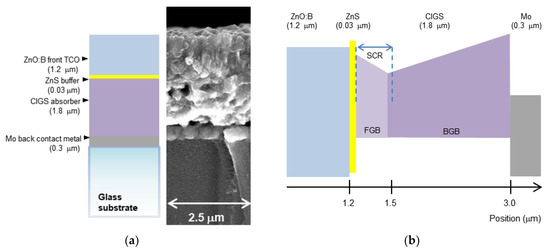
Figure 1.
Device structure: (a) scanning electron microscope (SEM) image of fabricated CIGS solar cell, and (b) schematic band structure for TCAD simulation, where FGB, BGB, and SCR are front gradient bandgap region, back gradient bandgap region, and space charge region, respectively.
The effects of the bandgap gradient on the CIGS solar cell conversion efficiency are investigated using a TCAD simulator (Synopsys Inc., Mountain View, USA). First, we characterized the simulation parameters such as thickness, carrier density, and material properties. Then, the thickness of each layer in the CIGS solar cell was measured by cross-sectional scanning electron microscopy and the carrier density in the CIGS layer was estimated by the capacitive-voltage method. The elemental composition in the CIGS layer was measured using secondary ion mass spectroscopy to calculate the Ga/(Ga + In) ratio as the gradient bandgap parameter. In order to apply the optical characteristics to the simulation, we modeled the absorption coefficient as a function of the Ga/(Ga + In) ratio by adopting the results from [12]. Because the bandgaps of the CIGS layers can be varied from 1.04 eV to 1.68 eV according to the Ga content, their optical parameters were also calculated with the bandgap, which was linearly interpolated. It is well known that the energy level, density, and shape of the defect states are important factors determining the minority carrier lifetime; particularly, VOC is strongly dependent on the minority carrier lifetime. Hanna et al. reported that the defect states in the CIGS layer consist of two types; the acceptor-like states of the Cu antisite and donor-like states of the Cu interstitial or In antisite [13]. Of these, we primarily considered the Cu antisite states in the simulation because the acceptor-like state in the p-type semiconductor is a dominant factor. The defect density of the CIGS layer as a function of Ga composition was also applied to the simulation. We referred to model B of the results of Frisk et al. [14]. We used a linear DGB structure of the CIGS layer with a ZnS buffer as [4,5,6], where the minimum bandgap of 1.1 eV is located at a depth of 0.25 μm in the CIGS from the interface of the ZnS buffer, and the maximum bandgap is 1.5 eV at a depth of 1.8 μm contacting the Mo layer as shown in Figure 1b. From the reference structure, we investigated the effects of the FGB and BGB on the CIGS solar cells.
3. Results and Discussion
In our CIGS solar cell, the Ga gradients were built on both the front and back of the CIGS layer. In order to apply the Ga gradient effect to the device simulation, we used the results of Wei et al.; the bandgap gradient effect of the CIGS layer by the variation of the Ga content mainly appears as an increase in the conduction band derived from first-principles bandgap theory [13]. In the simulation, the gradient bandgap profiles and electron affinities with various bandgaps were modeled numerically using Equations (1) and (2):
where Eg (x) and Chi (x) are the bandgap and electron affinity, respectively, and x is the Ga/(Ga + In) ratio in the CIGS layer. The defect model based on [15] is empirical, but it fits well to our experimental results. The other parameters were selected in a reasonable range or referred from a previous paper [16]. The main simulation parameters used in our simulations are listed in Table 1.
Eg (x) = −0.375 x2 + 1.1075 x + 0.98
Chi (x) = −0.475 x2 + 0.595 x + 4.48

Table 1.
Primary parameters of the materials in CIGS solar cell.
The electron and hole pairs generated by sunlight are separated and transferred to the opposite side. The movement of the carriers is greatly affected by the bandgap profile in the solar cells. The electron and hole pairs can be moved easily in the space charge region (SCR) where a high internal electric field is applied. Especially, the transportation of minority carriers in the CIGS absorption layer, and their movement over the band barrier at the interface of ZnS (due to electron affinity), are important causes for the conversion efficiency of the CIGS solar cells with ZnS buffer layers. Thus, the well-designed FGB of the CIGS layer could become the decisive factor determining the improvement in carrier transportation in the SCR. In particular cases, the FGB could disturb the carrier collection. Therefore, we investigated the conversion efficiency of the CIGS solar cell for the extent of the band gradient of the FGB structures. Figure 2 shows the conduction band and electron concentration profiles in the SCR of the CIGS at the steady state when the bandgap energies at the front edge are 1.1 eV, 1.18 eV, 1.24 eV, and 1.3 eV. The conduction band offset (CBO)—the mismatched alignment in the conduction band between the buffer and CIGS absorber layers—was measured from the J–V distortion curves under red light and dark illuminations [17]. We note that the shapes of the conduction band in Figure 2 were obtained from the J–V distortion measurement and the changes in CBO are very small for the front side bandgaps in our CIGS layers. The simulated results are presented in Figure 3 for the conversion efficiency parameters. As the front side bandgap increases from 1.1 eV to 1.37 eV, VOC gradually improves from 0.614 V to 0.648 V, but JSC and the fill factor (FF) decreases. As a result, the optimal front side bandgap is 1.18 eV in Figure 3. This can be attributed to the fact that the conduction band bending of the FGB helps the electrons to move over the band-offset of the ZnS interface barrier in the SCR for the low front side bandgap. However, for the high front side bandgap, a conduction band barrier forms near the interface of the ZnS buffer layer and disturbs the electron carrier transportation at the forward bias, so JSC and FF decreases gradually, as shown in Figure 3.
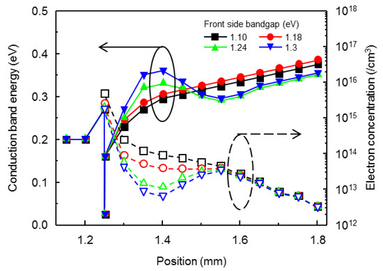
Figure 2.
Conduction band diagram and electron concentration at the position in CIGS cell as a function of the FGB.
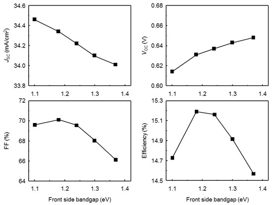
Figure 3.
Simulated solar cell conversion efficiency as a function of the front side bandgap: JSC, VOC, FF, Efficiency of CIGS solar cell with ZnS buffer layer as a function of front side bandgap.
The BGB for reducing the recombination at the back side was also investigated using the simulation. While the carriers generated near the front side can be quickly collected by the high internal electric field in the SCR, the carriers generated near the back side (absorbing long-wavelength photons) are slowly transferred and collected through carrier diffusion. The back side field of the BGB can assist in the carrier transportation to increase JSC and, consequently, VOC. Figure 4 shows the distributions of the electric field and extinction coefficient near the Mo interface layer as a function of the back side bandgap, and it numerically shows that the BGB generates an additional back side field to the front side, improving the electron transport. The simulated conversion efficiency parameters of the BGB CIGS cells are plotted in Figure 5 for the back side bandgap at the Mo interface. The solar cell conversion efficiency by bandgap gradient is combination effects of back side electrical field, extinction coefficient and defect density. As the back side bandgap increases from 1.32 eV to 1.57 eV, the gradient in the conduction band significantly increases the electric field from 2027 V/cm to 3197 V/cm, reducing the probability for carrier recombination at the back side, so that the solar cell conversion efficiency can be improved. As the bandgap (due to Ga/(Ga + In) ratio) increases, the extinction coefficient (the absorption coefficient of CIGS) of Figure 4 decreases, however, JSC improves by 0.4 mA/cm2 because of the back side field in the BGB, as shown in Figure 5. Additionally, FF consistently degrades with the increase in the bandgap because the influence of the defect density also increases. The back side bandgap grading should be optimized. The optimized value of the BGB is about 1.5 eV for achieving high efficiencies.
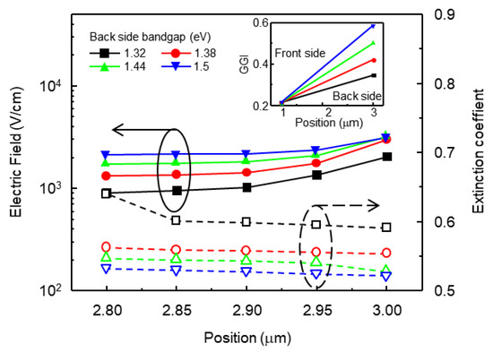
Figure 4.
Electric field and extinction coefficient at the position in CIGS cell as a function of the back side bandgap.

Figure 5.
Simulated solar cell conversion efficiency at the position in CIGS cell as a function of the back side bandgap: JSC, VOC, FF, Efficiency of CIGS solar cell with ZnS buffer layer as a function of back side bandgap.
We evaluated the conversion efficiency of the CIGS solar cells for four different bandgap gradient profiles, as shown in Figure 6. In addition to the DGB (the optimized one from the results of Figure 2 and Figure 4), a uniform (UNI) cell with no bandgap gradient, normal (NOR) cell only with the BGB, and reverse (REV) cell only with the FGB were simulated. Capacitance-voltage profiling (at 100 kHz, 50 mV) for the fabricated CIGS cell (DGB) was performed based on the approach in [9,10] acceptor (Na for p-CIGS) and donor (Nd for n-ZnS) concentrations were about 1.5 × 10¹⁶/cm3, and 1.5 × 10¹⁸/cm3, the depth of SCR was about 0.3 μm and capacitance was about 38.7 nF/cm2 at 0 V. Thus, for the comparison, we intentionally set the simulation parameters so the SCR ended at a depth of nearly 0.3 μm in the CIGS, and the average bandgap of the entire CIGS layer is about 1.27 eV for all the bandgap gradient structures shown in Figure 6 [18]. The conversion efficiencies of these solar cells are summarized in Table 2. Even though the average bandgap of the CIGS layer is approximately the same, the conversion efficiency of these solar cells is considerably different; the highest efficiency is obtained with the DGB and the lowest value is obtained with the REV solar cells.
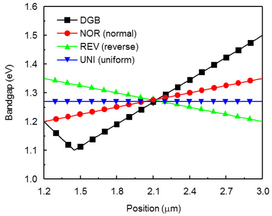
Figure 6.
Bandgap energy at the position in CIGS cell for the different bandgap profiles.
Table 2.
Performance of the experimented and simulated solar cells with different bandgap profiles.
From the results of Table 2, we found that VOC behaves very interestingly; there is a strong correlation between VOC and the average bandgap in the SCR rather than that of an entire CIGS layer. The average SCR bandgaps of the DGB, NOR, UNI, and REV cells are calculated as 1.144 eV, 1.212 eV, 1.270 eV, and 1.337 eV, respectively, which are strongly proportional to the VOC of the cells. Because the defect density is modeled as proportional to the bandgap (as a result of the Ga/(Ga + In) ratio), the defect density also increases with the bandgap: for example, the defect densities are 1.1 × 10¹⁴ /cm3 and 9.0 × 10¹⁴ /cm3 at the bandgap of 1.144 eV and 1.337 eV, respectively [15]. However, VOC further increases from 0.632 V to 0.730 V in Table 2 because the influence of the defect density is small in our model (in our cells). We note that VOC does not significantly degrade until the defect density of the SCR is much higher than 1.0 × 10¹⁵ /cm3 in our simulation.
As the DGB was determined to be the best bandgap gradient profile and VOC was selected within a desirable range using the average bandgap in SCR, we further investigated JSC and FF. We optimized the band structure of the DGB to obtain the best efficiency. To determine the main factor of JSC, we varied the individual parameters to simulate the DGB solar cell. For a ±10% variation in the minimum bandgap with the other parameters fixed, JSC changes by about ±0.7 mA/cm2, and the ±10% variation in back side bandgap changes JSC by about ±0.2 mA/cm2. Similarly, for the ±10% variation in the front side bandgap, JSC changes by about ±0.07 mA/cm2. The ±10% variation in defect density in the entire CIGS layer of the DGB structure causes JSC to change by ±1.2 mA/cm2. The FF is known to be affected by the bandgap as well as the defect density. In general, FF gradually declines when the front or back side bandgap exceeds a certain value, as shown in Figure 3 and Figure 5. The reduction of FF by the excessive front side bandgap is mainly attributed to the formation of the conduction band barrier obstructing electron collection, while the reduction by the excessive back side bandgap is because the defect traps become deeper as the bandgap increases with the Ga/(Ga + In) ratio [19,20]. Finally, based on the simulation results, we optimized the DGB structure for the CIGS solar cell incorporating the Cd-free ZnS buffer layer and fabricated the CIGS cells with a size of approximately 0.25 cm2. Figure 7 presents the simulated and measured current density-voltage curves under 1-sun illumination; the fabricated cell efficiency is about 15.2% and the simulated curve of the CIGS solar cell matches well with the experimental curve.
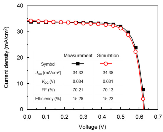
Figure 7.
Light current density-voltage curves of the experimental results (solid symbol) and simulation results (open symbol).
4. Conclusions
We numerically investigated the characteristics of the gradient bandgap profile in the absorption layer to evaluate the conversion efficiency of the CIGS solar cell with a Cd-free ZnS buffer layer using a TCAD simulation. The Ga-related parameters, such as defect density, bandgap, and electron affinity, can be controlled by the Ga/(Ga + In) ratio in the CIGS and were modeled and presented for the simulation. In the simulation, we considered the FGB, and the BGB formed by spatially varying the Ga content. The FGB enhanced the VOC, but the front side bandgap should be carefully designed to not disturb the electron transport at the conduction band barrier near the ZnS buffer layer. The BGB improved the electron transport at the back surface, but the excessive back side bandgap could induce the defect traps to move deeper in the CIGS, resulting in the degradation of the FF of the CIGS cell. By simulating the various types of band structures, DGB, NOR, REV, and UNI, we demonstrated that the DGB was the most effective structure for achieving the highest cell efficiency. We demonstrated that VOC strongly correlated with the average bandgap in the SCR and could be selected within the desirable range using the DGB; we also numerically evaluated JSC and FF for the band structural parameters of the CIGS cell. In this approach, we designed the optimal band structure of the CIGS cell with a Cd-free ZnS buffer layer and demonstrated a cell efficiency of more than 15% for the fabricated CIGS solar cells. The numerical design procedure of this work will be useful for developing high-conversion efficiency CIGS cells incorporating a gradient bandgap structure and Cd-free buffer layer.
Author Contributions
All authors contributed to this work. Conceptualization, simulation and analysis, J. Park.; Investigation, and supervision, M. Shin.
Funding
This work was supported by the Korea Institute of Energy Technology Evaluation and Planning (KETEP) and the Ministry of Trade, Industry & Energy (MOTIE) of the Republic of Korea (No. 20143030011530), and also supported by the Pioneer Research Center Program through the National Research Foundation of Korea funded by the Ministry of Science, ICT & Future Planning (NRF-2013M3C1A3065040).
Acknowledgments
This research was supported by the Solar Energy Group of the Samsung Electronics Inc.; the authors acknowledge the technical support and the assistance offered by Dr. Myeong-Woo Kim at the Samsung SDI. The authors also appreciate Dr. Dong-Seop Kim (Vice President of Samsung SDI) for his advice and leadership.
Conflicts of Interest
The authors declare no conflict of interest.
References
- Green, M.A.; Emery, K.; Hishikawa, Y.; Warta, W.; Dunlop, E.D. Solar cell efficiency tables (version 49). Prog. Photovolt. Res. Appl. 2016, 25, 3–13. [Google Scholar] [CrossRef]
- Kessler, F.; Herrmann, D.; Powalla, M. Approaches to flexible CIGS thin-film solar cells. Thin Solid Films 2005, 480, 491–498. [Google Scholar] [CrossRef]
- Nakada, T.; Mizutani, M.; Hagiwara, Y.; Kunioka, A. High-efficiency Cu(In,Ga)Se2 thin-film solar cells with a CBD-ZnS buffer layer. Solar Energy Mater. Solar Cells 2001, 67, 255–260. [Google Scholar] [CrossRef]
- Gloeckler, M.; Sites, J.R. Band-gap grading in Cu(In,Ga)Se2 solar cells. J. Phys. Chem. Solids 2005, 66, 1891–1894. [Google Scholar] [CrossRef]
- Song, J.; Li, S.S.; Huang, C.H.; Crisalle, O.D.; Anderson, T.J. Device modeling and simulation of the performance of Cu(In1−x,Gax)Se2 solar cells. Solid-State Electronics 2004, 48, 73–79. [Google Scholar] [CrossRef]
- Song, S.H.; Nagaich, K.; Aydil, E.S.; Feist, R.; Haley, R.; Campbell, S.A. Structure optimization for a high efficiency CIGS solar cell. In Proceedings of the 2010 35th IEEE Photovoltaic Specialists Conference, Honolulu, HI, USA, 20–25 June 2010; pp. 2488–2492. [Google Scholar]
- Dullweber, T.; Lundberg, O.; Malmstörm, J.; Bodegård, M.; Stolt, L.; Rau, U.; Schock, H.W.; Werner, J.H. Werner Back surface band gap gradings in Cu(In,Ga)Se2 solar cells. Thin Solid Films 2001, 387, 11–13. [Google Scholar] [CrossRef]
- Sozzi, G.; Troni, F.; Menozzi, R. On the combined effects of window/buffer and buffer/absorber conduction-band offsets, buffer thickness and doping on thin-film. Sol. Energy Mater. Sol. Cells 2014. [Google Scholar] [CrossRef]
- Heo, S.; Lee, H.-I.; Song, T.; Park, J.-B.; Ko, D.-S.; Chung, J.; Kim, K.; Kim, S.H.; Yun, D.-J.; Ham, Y.; et al. Direct band gap measurement of Cu(In,Ga)(Se,S)2 thin films using high-resolution reflection electron energy loss spectroscopy. Appl. Phys. Lett. 2015, 106. [Google Scholar] [CrossRef]
- Lee, D.; Yang, J.Y.; Kim, Y.-S.; Mo, C.B.; Park, S.; Kim, B.J.; Kim, D.; Nam, J.; Kang, Y. Effects of the Cu/(Ga + In) ratio on the bulk and interface properties of Cu(InGa)(SSe)2 solar cells. Sol. Energy Mater. Sol. Cells 2016, 149, 195–203. [Google Scholar] [CrossRef]
- Luber, E.J.; Buriak, J.M. Reporting performance in organic photovoltaic devices. ACS Nano 2013, 7, 4708–4714. [Google Scholar] [CrossRef] [PubMed]
- Durante Rincón, C.A.; Hernández, E.; Alonso, M.I.; Garriga, M.; Wasim, S.M.; Rincón, C.; León, M. Optical transitions near the band edge in bulk CuInxGa1−xSe2 from ellipsometric measurements. Mater. Chem. Phys. 2001, 70, 300–304. [Google Scholar] [CrossRef]
- Wei, S.-H.; Zhang, S.B.; Zunger, A. Effects of Ga addition to CuInSe2 on its electronic, structural, and defect properties. Appl. Phys. Lett. 1998, 72, 3199–3201. [Google Scholar] [CrossRef]
- Frisk, C.; Platzer-Björkman, C.; Olsson, J.; Szaniawski, P.; Wätjen, J.T.; Fjällström, V.; Salomé, P.; Edoff, M. Optimizing Ga-profiles for highly efficient Cu(In,Ga)Se2 thin film solar cells in simple and complex defect models. J. Phys. D Appl. Phys. 2014, 47, 485104–485115. [Google Scholar] [CrossRef]
- Hanna, G.; Jasenek, A.; Rau, U.; Schock, H.W. Influence of the Ga-content on the bulk defect densities of Cu(In, Ga)Se2. Thin Solid Films 2001, 387, 71–73. [Google Scholar] [CrossRef]
- Gloeckler, M.; Fahrenbruch, A.L.; Sites, J.R. Numerical modeling of CIGS and CdTe solar cells: setting the baseline. Proc. 3rd World Conf. Photovolt. Energy Conversion 2003, 1, 491–494. [Google Scholar] [CrossRef]
- Pudov, A.O.; Kanevce, A.; Al-Thani, H.A.; Sites, J.R.; Hasoon, F.S. Secondary barriers in CdS-CuIn1−xGaxSe2 solar cells. J. Appl. Phys. 2005, 97, 064901. [Google Scholar] [CrossRef]
- Barkhouse, D.A.R.; Gunawan, O.; Gokmen, T.; Todorov, T.K.; Mitzi, D.B. Device characteristics of a 10.1% hydrazine-processed Cu2ZnSn(Se,S)4 solar cell. Prog. Photovolt. 2012, 20, 6–11. [Google Scholar] [CrossRef]
- Heath, J.T.; Cohen, J.D.; Shafarman, W.N.; Liao, D.X.; Rockett, A.A. Effect of Ga content on defect states in CuIn1−xGaxSe2 photovoltaic devices. Appl. Phys. Lett. 2002, 80, 4540–4542. [Google Scholar] [CrossRef]
- Cao, Q.; Gunawan, O.; Copel, M.; Reuter, K.B.; Chey, S.J.; Deline, V.R.; Mitzi, D.B. Defects in Cu(In,Ga)Se2 chalcopyrite semiconductors: A comparative study of material properties, defect states, and photovoltaic performance. Adv. Energy Mater. 2011, 1, 845–853. [Google Scholar] [CrossRef]
© 2018 by the authors. Licensee MDPI, Basel, Switzerland. This article is an open access article distributed under the terms and conditions of the Creative Commons Attribution (CC BY) license (http://creativecommons.org/licenses/by/4.0/).