Article

Area-Saving and High-Efficiency RGB LED Driver with Adaptive Driving Voltage and Energy-Saving Technique

by
Yi-Chieh Hsu
1,
Jing-Yuan Lin
2,* and
Charlie Chung-Ping Chen
1
1
Graduate Institute of Electronics Engineering, and Department of Electrical Engineering, National Taiwan University, Taipei 10607, Taiwan
2
Department of Electronic and Computer Engineering, National Taiwan University of Science and Technology, Taipei 10607, Taiwan
*
Author to whom correspondence should be addressed.
Energies 2018, 11(6), 1422; https://doi.org/10.3390/en11061422
Submission received: 26 April 2018 / Revised: 29 May 2018 / Accepted: 30 May 2018 / Published: 1 June 2018
(This article belongs to the Section F: Electrical Engineering)

Abstract

:
The red-green-blue light-emitting diode (RGBLED) driver with adaptive driving voltage and energy-saving (ADVE) technique is presented in this paper. To obtain the proper driving voltage, a dynamic output voltage selector is proposed. This approach tracks the reference voltage of a boost converter to achieve the appropriate output voltage of the boost converter. Hence, the power loss of the linear current regulator is reduced to improve the efficiency of whole system. Moreover, the chip area is saved by the proposed switching linear current regulator. This chip was fabricated using TSMC 0.35 μm 2P4M complementary metal-oxide-semiconductor (CMOS) technology. The active chip area is 0.3 mm2. The maximum driving current and operating frequency are 100 mA and 100 kHz, respectively. Compared with a conventional LED driver with fixed output voltage, the experimental results demonstrate that the power loss of the proposed LED driver with ADVE technique is reduced by over 58%.

Graphical Abstract

1. Introduction

Light emitting diodes (LEDs) have been widely used in lighting and backlight units (BLUs) due to their long lifespan, high reliability, good gamut, and energy efficiency [1,2,3,4,5]. For example, the power consumption of the LED BLU in liquid crystal display (LCD) panels is reduced by 40% compared with the conventional cold cathode fluorescent lamp (CCFL) BLU [6].
LEDs have been gradually improved by technological advances. The advances in the LED field can be attributed to the significant improvement in III-nitride–based device efficiency [7,8]. Specifically, the internal quantum efficiency of LEDs has been extensively researched and improved in recent years. The internal quantum efficiency of InGaN LEDs has been improved by use of the large overlap quantum well concept [9,10,11], and the light extraction efficiency of LEDs has been improved by use of the surface roughening technique [12] and microsphere arrays [13,14].
White LEDs and red-green-blue (RGB) LEDs are two popular sources of BLUs. First, white LEDs can directly emit white light. However, the white LED driver usually requires color filters in LCD operation mode. As a result, the LED driver is less efficient. Another source of BLUs is RGBLEDs. By using an RGBLED driver with the field-sequential-color (FSC) technique [15,16], the color filters can be eliminated. The operating principle of FSC is depicted in Figure 1.
An LED driver consists of a power stage and LED strings. In order to obtain sufficient voltage to drive LED strings, the selection of power stage is significant. A charge pump, as shown in Figure 2, is a kind of inductorless DC–DC converter that uses capacitors as energy storage components to generate ahigher or lower voltage source [17]. It is applied to low-power circuits because of its poor efficiency,such as in flashlights in portable devices and memory circuits [18]. To achieve high conversion efficiency in medium- or high-power applications, such as lighting and backlighting for LCD displays, inductor-based boost DC–DC converters are usually employed [19].
The luminance of LEDs is proportional to forward current [20]. Hence, current regulators are employed to ensure current accuracy. In addition, to guarantee sufficient luminance, parallel and series LED strings are used. However, each LED probably has a different forward voltage due to the process variation, use time, and environmental temperature [21,22]. This phenomenon leads to redundant voltages across linear current regulators. As a result, the power consumption of the LED driver gradually increases.
The conventional RGBLED driver provides a constant output voltage to the RGBLED strings, but the forward voltage of red, green, and blue LEDs is different, as shown in Figure 3. In general, the forward voltage of a green or blue LED is larger than that of a red LED [23]. Figure 4 illustrates a conventional RGBLED driver. To ensure uniform brightness, current regulators are usually used. However, redundant voltage across linear current regulators leads to additional power loss. To minimize the voltage across linear current regulators, adaptive voltage control was introduced (Figure 5) [24,25,26,27,28,29]. This approach can suppress the power loss of a linear current regulator using a minimum voltage selection circuit. However, the output voltage is determined by the larger forward voltage LEDs. The redundant voltage still occurs across the linear current regulator of the lower forward voltage LED string. As a result, the efficiency of the improvement is limited. Furthermore, each LED string requires a linear current regulator and external compensating components so that the chip area is significantly occupied. Some other approaches have used diodes [24,25,26] and bipolar junction transistors [27] as minimum voltage selection circuits, which may not be able to be implemented in a standard CMOS process. Thus, these approaches may be inappropriate for an integrated circuit.
This paper presents an adaptive driving voltage and energy-saving (ADVE) technique. The output voltage of a DC–DC converter can be easily adjusted to minimize the voltage across the linear current regulator to save chip area. The remainder of the paper is structured as follows. In Section 2, the proposed LED driver is introduced. The circuit implementation of the proposed LED driver isoutlinedin Section 3, and the experimental results are provided in Section 4. Finally, our conclusions are detailed in Section 5.

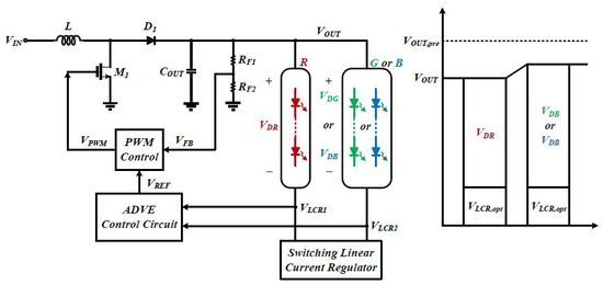
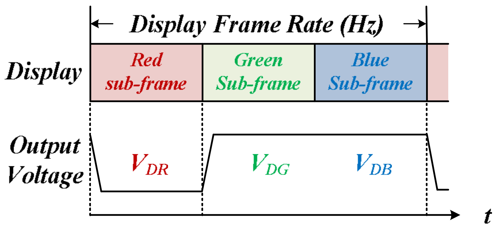
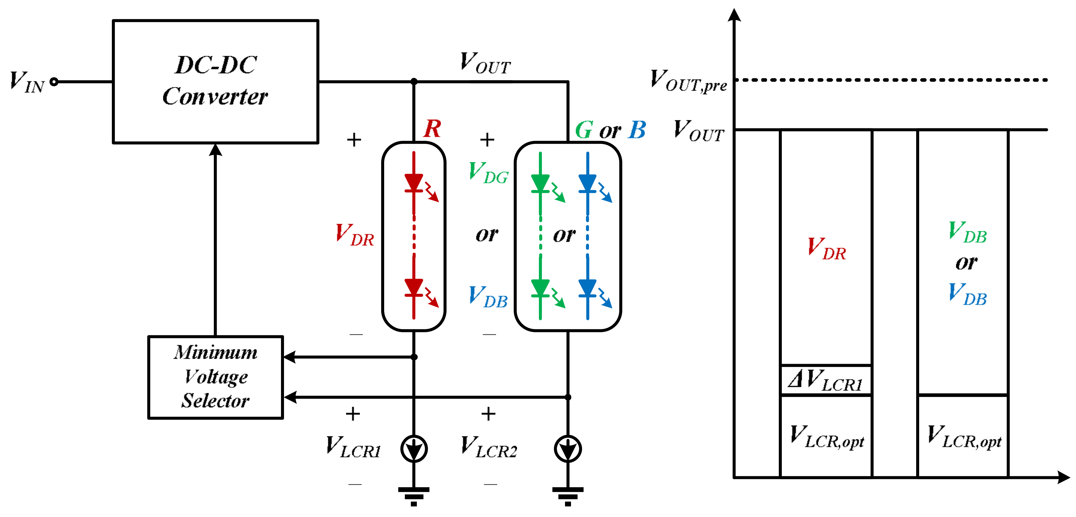
2. Proposed Adaptive Driving Voltage and Energy-Saving Technique

A block diagram and the operating principle of the LED driver with the ADVE technique are depicted in Figure 6. The main functional blocks of the proposed LED driver include the boost DC–DC converter, pulse-width modulation (PWM) control circuit, ADVE control circuit, and switching linear current regulator. The boost converter is used to obtain sufficient output voltage VOUT for the LED strings and can be expressed as:
V O U T = V D + V L C R
where VD and VLCR are the forward voltage of the LED and voltages across the linear current regulators, respectively.
When the ADVE is disabled, the voltages across the linear current regulators VLCR can be written as:
V L C R = V L C R + V L C R , o p t
where ∆VLCR and VLCR,opt are the redundant voltage across the switching linear current regulator and the minimum operating voltage of the switching linear current regulator, respectively. The redundant voltage ∆VLCR across the linear current regulator may cause unexpected power loss, which can be determined as:
P L o s s = I L E D ( V L C R + V L C R , o p t )
When the ADVE is used, the ADVE control circuit will detect any deviation in the forward voltage of the LED strings. Hence, the reference voltage of the boost converter can be adaptively adjusted. Finally, the PWM control circuit generates the corresponding duty cycle to change the output voltage. The optimized power loss of the linear current regulator can be calculated as:
P L o s s , o p t = I L E D × V L C R , o p t
For example, the PWM control circuit generates a wider duty cycle when the ADVE control circuit detects lower voltage across the switching linear current regulator. The boost converter output voltage can be increased, and vice versa. Compared with the previous output voltage VOUT,pre, the modified output voltage VOUT is appropriate to drive LED strings.

3. Circuit Implementation

The proposed LED driver with the ADVE technique and its implementation are described in this section.

3.1. Switching Linear Current Regulators

Linear current regulators are needed to obtain accurate driving current for LED strings. Figure 7 depicts a traditional current regulator. A linear current regulator [30] is shown in Figure 7a, composed of a power transistor M1, an operational amplifier, and a sensing resistor RS. The operational amplifier input voltage VREF is provided. Due to the negative feedback configuration of the operational amplifier, the voltage across the sensing resistor VREF is equal to the VS. A current ILED is generated and is expressed as:
I L E D = V R E F / R S = V S / R S
Another method for current regulation, shown in Figure 7b, is the current mirror [31]. The current accuracy is not guaranteed with this mechanism because of the transistor M2 and power transistor M3 mismatch. However, multiple linear current regulators should be used because of the multiple LED strings with output. The power consumption and the chip area increase. As a result, the whole system efficiency decreases. The proposed switching linear current regulator is shown in Figure 8a, consisting of an operational amplifier, a multiplexer, two power transistors M1 and M2, two assistant transistors M3 and M4, two sensing resistors RSENSE1 and RSENSE2, and two transmission gates TG1 and TG2. To create the negative feedback configuration of the operational amplifier, the voltages across the sensing resistors VSENSE1 and VSENSE2 are equal to the input voltage VCONST. Therefore, we obtain the driving current ILED1 and ILED2. They can be determined as:
I L E D 1 = V C O N S T / R S E N S E 1
I L E D 2 = V C O N S T / R S E N S E 2
To save chip area, an operational amplifier is used. The driving currents ILED1 and ILED2 alternatively use the operational amplifier by the selection signal VSEL. To satisfy the display frame rate of the FSC algorithm, the VSEL was set as 60 Hz. The multiplexer and the transmission gates are used to switch the multiple LED string driving current. When the selection signal VSEL is high, as shown in Figure 8b, the transmission gate TG1 is chosen. The multiplexer connects to the source of the power transistor M1 to form the negative feedback configuration. The assistant transistor M4 is turned on to prevent the glitch. The transmission gate TG2 is selected when the selection signal is low,as shown in Figure 8c. The source of the power transistor M2 is connected to the multiplexer and the negative feedback configuration is formed. To preclude the glitch, the assistant transistor M3 is turned on.

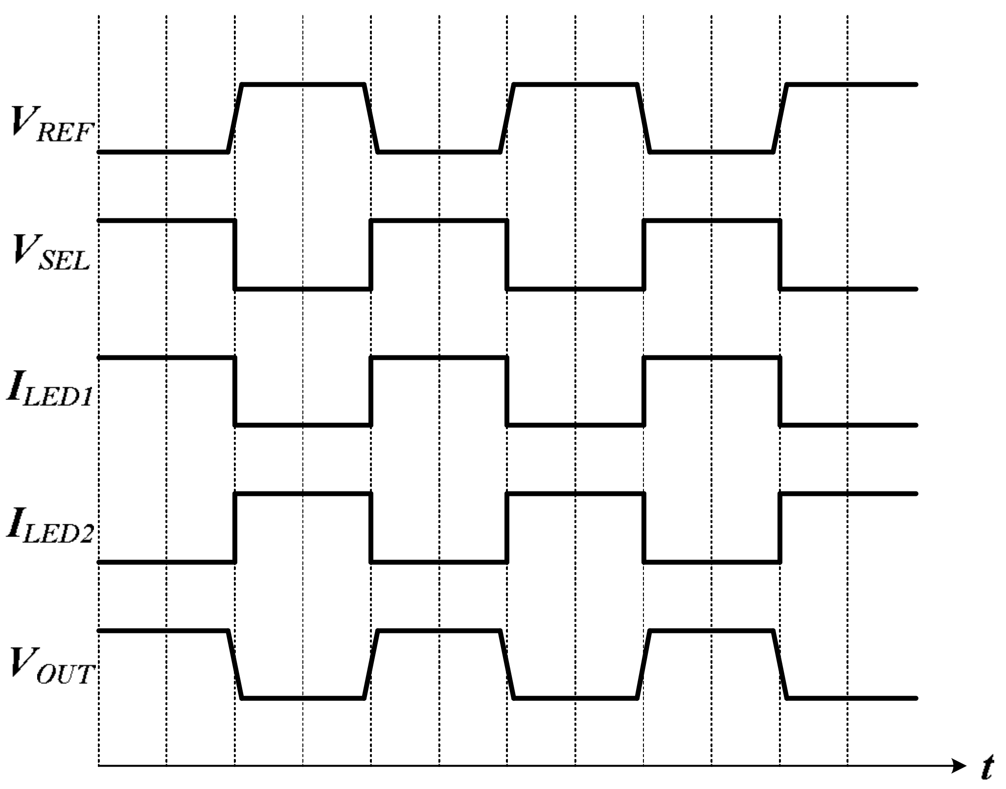
3.2. Adaptive Driving Voltage and Energy-Saving Control Circuit

Figure 9 depicts the proposed ADVE control circuit. VLCR1 and VLCR2 are the voltages across the switching linear current regulator. According to the selection signal VSEL, the multiplexer can acquire the drain voltage of the switching linear current regulator to the operational transconductance amplifier (OTA). The error amplification is formed by the voltage across the switching linear current regulator VLCR1, VLCR2, and the minimum operating voltage of the switching linear current regulator VLCR,opt to modify the boost converter reference voltage. Thus, the boost converter output voltage can be adjusted. The operating waveform for the ADVE technique is shown in Figure 10.

3.3. Sawtooth Generator

We used a sawtooth generator [32] to generate a sawtooth wave for the PWM control circuit. Figure 11 illustrates the sawtooth generator, composed of a V-I converter and a hysteretic comparator. Given the operational amplifier negative feedback configuration, the input voltage VIN_SAW is equal to the voltage across the resistor VT. The current IT is generated and can be calculated as:
I T = V I N _ S A W / R T = V T / R T
The current IT is replicated by the current mirrors M2 and M3 to charge the capacitor CT. When the capacitor CT voltage is larger than the upper threshold voltage VUP, the transistor M4 turns on using the SR latch to instantaneously discharge the capacitor CT. The transistor M4 is turned off using the SR latch when the capacitor CT voltage is smaller than the lower threshold voltage VDN. Thus, the capacitor CT is charged again by the current IT. The periodic operation can obtain the sawtooth wave. According to the above operating principle, we determine the capacitor CT charge. It can be expressed as:
Q = I T / f = C T ( V U P V D N )
When the upper threshold voltage VUP is equal to the sum of the lower threshold voltage VDN and input voltage VIN_SAW, we can determine:
f = 1 / C T R T
where f is the sawtooth generator oscillation frequency.

3.4. PWM Control Circuit

The PWM control circuit is shown in Figure 12. First, the OTA is usedas the error amplifier. The feedback of the output voltage is VFB and the reference voltage is VREF is the error amplifier input. The stability of the whole systemrequires the external components RZ and CC with the error amplifier output. They generate the error signal VEA to the comparator, which is compared to the sawtooth wave VSAW. The comparator output then produces a PWM signal to the gate-driving buffer to drive the boost converter power transistor.

4. Experimental Results

To verify the proposed ADVE technique performance, the chip was implemented using TSMC 0.35 μm 2P4M CMOS technology. The chip microphotograph is shown in Figure 13. The proposed LED driver specifications include an input voltage of 5–7 V, output voltage of 8–14 V, operating frequency of 100 kHz, and maximum driving current of 100 mA. The proposed LED driver performance is compared to prior methods in Table 1.
The measured output voltage waveforms, voltages across the LEDs, and driving currentsof LED string1 and string2 are shown in Figure 14 and Figure 15, respectively. The waveform demonstrates that the forward voltages, VLED1 and VLED2, of the LED strings are different. Therefore, the output voltage VOUT can be dynamically adjusted to reduce the switching linear current regulator power consumption. The LED string currents ILED1 and ILED2 are constant when the corresponding linear current regulator is turned on.
Figure 16 compares the switching linear current regulator power loss with and without the ADVE technique. When the driving current is different, the proposed ADVE technique can dynamically regulate the output voltage. Compared with the conventional LED driver with fixed output voltage, the voltage across the switching linear current regulator is minimized and the power loss of the switching linear current regulator is suppressed by over 58%.

5. Conclusions

This paper presents an RGBLED driver with the ADVE technique. To acquire the appropriate driving voltage for LED strings, a dynamic output voltage selector is proposed. This approach tracks the reference voltage of the boost converter to reach the proper output voltage of the boost converter. Thus, the power loss of the linear current regulators is suppressed to improve the efficiency of the entire system. In addition, chip area is saved by means of the proposed switching linear current regulator. The chip is implemented using the TSMC 0.35 μm 2P4M CMOS process. The active chip area is 0.3 mm2. The maximum driving current and operating frequency are 100 mA and 100 kHz, respectively. Compared to conventional LED drivers with fixed output voltage, the experimental results show that the power loss of our proposed LED driver with ADVE technique is reduced by over 58%.

Author Contributions

Y.-C.H. and J.-Y.L. conceived and designed the architecture and experiment. Y.-C.H. performed the experiment and wrote the paper. J.-Y.L. and C.C.-P.C. provided all material for the experiment, and supervised the design, analysis, and experiment and editing of the paper.

Funding

This research received no external funding.

Acknowledgments

The authors would like to thank the National Chip Implementation Center (CIC) Taiwan for chip fabrication and technical support.

Conflicts of Interest

The authors declare no conflict of interest.

References

  1. Thielemans, S.; Zenobio, D.D.; Touhafi, A.; Lataire, P.; Steenhaut, K. DC Grids for Smart LED-Based Lighting: The EDISON Solution. Energies 2017, 10, 1454. [Google Scholar] [CrossRef]
  2. Vu, N.H.; Pham, T.T.; Shin, S. LED Uniform Illumination Using Double Linear Fresnel Lenses for Energy Saving. Energies 2017, 10, 2091. [Google Scholar] [CrossRef]
  3. Lin, Y.-L.; Chiu, H.-J.; Lo, Y.-K.; Leng, C.-M. LED Backlight Driver Circuit With Dual-Mode Dimming Control and Current-Balancing Design. IEEE Trans. Ind. Electron. 2014, 61, 4632–4639. [Google Scholar] [CrossRef]
  4. Ahn, Y.D.; Bae, S.; Kang, S.-J. Power Controllable LED System with Increased Energy Efficiency Using Multi-Sensors for Plant Cultivation. Energies 2017, 10, 1607. [Google Scholar] [CrossRef]
  5. Lin, M.-S.; Chen, C.-L. An LED Driver with Pulse Current Driving Technique. IEEE Trans. Power Electron. 2012, 27, 4594–4601. [Google Scholar] [CrossRef]
  6. Hsieh, C.-Y.; Chen, K.-H. Boost DC–DC Converter with Fast Reference Tracking (FRT) and Charge-Recycling (CR) Techniques for High-Efficiency and Low-Cost LED Driver. IEEE J. SolidState Circuits 2009, 44, 2568–2580. [Google Scholar] [CrossRef]
  7. Crawford, M. LEDs for Solid-State Lighting: Performance Challenges and Recent Advances. IEEE J. Sel. Top. Quantum Electron. 2009, 15, 1028–1040. [Google Scholar] [CrossRef]
  8. Tansu, N.; Zhao, H.; Liu, G.; Li, X.-H.; Tong, J.-Z.; Tong, H.; Ee, Y.-K. III-Nitride Photonics. IEEE Photonics J. 2010, 2, 241–248. [Google Scholar] [CrossRef]
  9. DenBaars, S.; Feezell, D.; Kelchner, K.; Pimputkar, S.; Pan, C.-C.; Yen, C.-C.; Tanaka, S.; Zhao, Y.; Pfaff, N.; Farrell, R.; et al. Development of Gallium-nitride-based Light-emitting diodes (LEDs) and Laser Diodes for Energy-efficient Lighting and Displays. Acta Mater. 2013, 61, 945–951. [Google Scholar] [CrossRef]
  10. Arif, R.A.; Ee, Y.-K.; Tansu, N. Polarization Engineering via Staggered InGaN Quantum Wells for Radiative Efficiency Enhancement of Light Emitting Diodes. Appl. Phys. Lett. 2007, 91, 091110. [Google Scholar] [CrossRef]
  11. Tan, C.-K.; Tansu, N. Nanostructured Lasers: Electrons and Goles Get Closer. Nat. Nanotechnol. 2015, 10, 107–109. [Google Scholar] [CrossRef] [PubMed]
  12. Park, H.-H.; Zhang, X.; Cho, Y.; Kim, D.-W.; Kim, J.; Lee, K.-W.; Choi, J.; Lee, H.-K.; Jung, S.-H.; Her, E.-J.; et al. Wafer-scale Surface Roughening for Enhanced Light Extraction of High Power AlGaInP-based Light-emitting Diodes. Opt. Express 2014, 22, A723–A734. [Google Scholar] [CrossRef] [PubMed]
  13. Zhu, P.-F.; Tansu, N. Effect of Packing Density and Packing Geometry on Light Extraction of III-Nitride Light-Emitting Diodes with Microsphere Arrays. Photonics Res. 2015, 3, 184–191. [Google Scholar] [CrossRef]
  14. Li, X.-H.; Zhu, P.-F.; Liu, G.-Y.; Zhang, J.; Song, R.-B.; Ee, Y.-K.; Kumnorkaew, P.; Gilchrist, J.-F.; Tansu, N. Light Extraction Efficiency Enhancement of III-Nitride Light-Emitting Diodes by using 2-D Close-Packed TiO2 Microsphere Arrays. IEEE J. Disp. Technol. 2013, 9, 324–332. [Google Scholar] [CrossRef]
  15. Yamada, F.; Nakamura, H.; Sakaguchi, Y.; Taira, Y. Sequentialcolor LCD based on OCB with an LED backlight. J. SID 2002, 10, 81–85. [Google Scholar]
  16. Chen, C.-C.; Wu, C.-Y.; Chen, Y.-M.; Wu, T.-F. Sequential Color LED Backlight Driving System for LCD Panels. IEEE Trans. Power Electron. 2007, 22, 919–925. [Google Scholar] [CrossRef]
  17. Wu, C.-H.; Chen, C.-L. High-Efficiency Current-Regulated Charge Pump for a White LED Driver. IEEE Trans. Circuits Syst. II Exp. Briefs 2009, 56, 763–767. [Google Scholar]
  18. Fu, L.; Wang, Y.; Wang, Q.; Yang, S.; Yang, Y.; Huo, Z. A High Efficiency All-PMOS Charge Pump for 3D NAND Flash Memory. In Proceedings of the IEEE 11th International Conference on ASIC (ASICON), Chengdu, China, 3–6 November 2015; pp. 1–4. [Google Scholar]
  19. Hsieh, C.-Y.; Yang, C.-Y.; Chen, K.-H. A Charge-Recycling Buck-Store and Boost-Restore (BSBR) Technique with Dual Outputs for RGB LED Backlight and Flashlight Module. IEEE Trans. Power Electron. 2009, 24, 1914–1925. [Google Scholar] [CrossRef]
  20. Lun, W.-K.; Loo, K.-H.; Tan, S.-C.; Lai, Y.-M.; Tse, C.-K. Bilevel Current Driving Technique for LEDs. IEEE Trans. Power Electron. 2009, 24, 2920–2932. [Google Scholar]
  21. Liu, C.-H.; Hsieh, C.-Y.; Hsieh, Y.-C.; Tai, T.-J.; Chen, K.-H. SAR-Controlled Adaptive Off-Time Technique Without Sensing Resistor for Achieving High Efficiency and Accuracy LED Lighting System. IEEE Trans. Circuits Syst. I Reg. Pap. 2010, 57, 1384–1394. [Google Scholar]
  22. Van der Broeck, H.; Sauerlander, G.; Wendt, M. Power Driver Topologies and Control Schemes for LEDs. In Proceedings of the IEEE Applied Power Electronics Conference and Exposition (APEC), Anaheim, CA, USA, 25 February–1 March 2007; pp. 1319–1325. [Google Scholar]
  23. Seoul Semiconductor Co. Ltd. SZX05A0A Z-Power LED, SSC-SZX05A0A Datasheet. Available online: https://docs-emea.rs-online.com/webdocs/1009/0900766b810099d0.pdf (accessed on April 2017).
  24. Hu, Y.; Jovanovic, M. LED Driver with Self-Adaptive Drive Voltage. IEEE Trans. Power Electron. 2008, 23, 3116–3125. [Google Scholar] [CrossRef]
  25. Chiu, H.-J.; Lo, Y.-K.; Chen, J.-T.; Cheng, S.-J.; Lin, C.-Y.; Mou, S.-C. A High-Efficiency Dimmable LED Driver for Low-Power Lighting Applications. IEEE Trans. Ind. Electron. 2010, 57, 735–743. [Google Scholar] [CrossRef] [Green Version]
  26. Liu, P.-J.; Hsu, S.-R.; Chang, C.-W.; Chien, L.-H. Dimmable White LED Driver with Adaptive Voltage Feedback Control. In Proceedings of the IEEE International Future Energy Electronics Conference (IFEEC), Taipei, Taiwan, 1–4 November 2015; pp. 1–4. [Google Scholar]
  27. Hong, S.-I.; Han, J.-W.; Kim, D.-H.; Kwon, O.-K. A Double-loop Control LED Backlight Driver IC for Medium-sized LCDs. In Proceedings of the IEEE ISSCC, San Francisco, CA, USA, 7–11 February 2010; pp. 116–117. [Google Scholar]
  28. Sun, Y.-M.; Wu, X.-B. High Efficiency LED Driver Featuring Auto Output-voltage Tuning. In Proceedings of the 2010 IEEE International Conference of Electron Devices and Solid-State Circuits (EDSSC), Hong Kong, China, 15–17 December 2010; pp. 1–4. [Google Scholar]
  29. Hsieh, Y.-T.; Liu, B.-D.; Wu, J.-F.; Fang, C.-L.; Tsai, H.-H.; Juang, Y.-Z. A High-dimming-ratio LED Driver for LCD Backlights. IEEE Trans. Power Electron. 2012, 27, 4562–4570. [Google Scholar] [CrossRef]
  30. Allen, P.E.; Holberg, D.R. CMOS Analog Circuit Design, 2nd ed.; Oxford University Press: New York, NY, USA, 2002; p. 157. ISBN 0195392469. [Google Scholar]
  31. Baker, R.J. CMOS Circuit Design, Layout, and Simulation, 2nd ed.; IEEE Press: Piscataway, NJ, USA, 2005; p. 645. ISBN 047170055X. [Google Scholar]
  32. Lee, C.-F.; Mok, P.-K.-T. A Monolithic Current-Mode CMOS DC-DC Converter with on-Chip Current-Sensing Technique. IEEE J. SolidState Circuits 2004, 39, 3–14. [Google Scholar] [CrossRef]
Figure 1. Concept of frequency-sequential-color technique.
Energies 11 01422 g001
Figure 2. Schematic of a light-emitting diode (LED) driver with charge pump.
Energies 11 01422 g002
Figure 3. Different forward voltages of red-green-blue (RGB)LEDs under the same driving current.
Energies 11 01422 g003
Figure 4. Conventional LED driver.
Energies 11 01422 g004
Figure 5. LED driver with adaptive driving voltage control technique.
Energies 11 01422 g005
Figure 6. Proposed LED driver with adaptive driving voltage and energy-saving (ADVE) technique.
Energies 11 01422 g006
Figure 7. Constant current source with (a) a linear current regulator and (b) a current mirror.
Energies 11 01422 g007
Figure 8. Proposed switching linear current regulator: (a) schematic; (b) driving current path of LED string1; (c) driving current path of LED string2.
Energies 11 01422 g008
Figure 9. Proposed adaptive driving voltage and energy-saving control circuit.
Energies 11 01422 g009
Figure 10. Operating waveform of proposed adaptive driving voltage and energy-saving control circuit.
Energies 11 01422 g010
Figure 11. Sawtooth wave generator.
Energies 11 01422 g011
Figure 12. Pulse-width modulation (PWM) control circuit.
Energies 11 01422 g012
Figure 13. Chip microphotograph.
Energies 11 01422 g013
Figure 14. Measured waveform of LED string1.
Energies 11 01422 g014
Figure 15. Measured waveform of LED string2.
Energies 11 01422 g015
Figure 16. Power loss comparison with and without ADVE technique.
Energies 11 01422 g016
Table 1. Performance comparison.
Specifications[5][17][26][27]This Work
Technology0.35 μm CMOS0.5 μm CMOS0.35 μm CMOS0.35 μm BCD0.35 μm CMOS
Active Area (mm2)0.890.403N/AN/A0.3
Input Voltage (V)4.5~52.8~4.276~275~7
Output Voltage (V)N/A2.8~4.210~14608~14
Driving Capability1 LED1 LEDN/A24 LEDs6~8 LEDs
Driving Current (mA)2202020030100
Operating Freq. (kHz)50020010039100
Adaptive ControlNoNoYesYesYes
Energy-Saving ControlNoNoNoNoYes

