Article

A Multiple Legs Inverter with Real Time–Reflected Load Detection Used in the Dynamic Wireless Charging System of Electric Vehicles

College of Optoelectronic Engineering, Shenzhen University, Shenzhen 518060, China
*
Author to whom correspondence should be addressed.
Energies 2018, 11(5), 1275; https://doi.org/10.3390/en11051275
Submission received: 19 March 2018 / Revised: 11 May 2018 / Accepted: 12 May 2018 / Published: 16 May 2018
(This article belongs to the Section F: Electrical Engineering)

Abstract

:
Dynamic wireless power transfer is a potentially effective method to solve issues related to the range anxiety of electric vehicles (EVs) and reduce the cost of on-board batteries. A novel multiple legs inverter topology with a reflected load identification method for dynamic EV charging is proposed in this paper. In the proposed circuit topology, several inductor-capacitor-capacitor (LCC) reactive power compensation resonant networks and primary pads are selectively excited through a sole primary converter. Besides, a high-response and simple method for the reflected load identification is proposed to rapidly and precisely detect the EV’s position, providing accurate power regulation reference to the converter. With the proposed method, the system can realize high-response and closed-loop power control precisely without any additional wireless communication and position detection devices. Simulation and experimental results verified the efficiency of the proposed scheme. Additionally, the cost comparison results reveal that the proposed scheme could reduce costs by nearly 78% in comparison with the conventional scheme.

1. Introduction

Electrification in the transportation sector has been strongly emphasized in the last decades due to tougher regulations triggered by environmental concerns and energy security concerns [1]. For electric vehicles (EVs), a high power and large capacity battery pack is equipped as the energy storage unit for an extended range, which increases the cost and dead-weigh of EVs [2].
To mitigate the battery cost and cruising ability issues, wireless power transfer (WPT) for EV charging has been extensively studied and has begun to be commercialized in recent years. Numerous charging types (such as inductive, magnetic resonant, and energy collection) and different coupling modes (such as stationary charging and dynamic charging) for WPT system had been proposed [3]. Among these different modes, the dynamic wireless charging with magnetic resonant charging type promises to significantly extend the vehicle mileage, decrease battery size, and improve the power density. In this mode, the EVs can be online charged while they are moving over charging tracks or pads [4], which are installed underground. By using dynamic wireless charging, journey idle time due to stops for charging decreases, and the ratio of distance over battery size increases, so smaller battery packs could be feasible.
There are two distinctive designs for primary magnetic couplers in dynamic charging, including distributed elongate track and pads array. To track couplers, continuous power can be transferred wirelessly from a long primary track to the receiver when the EV is running along the track [5,6,7,8]. However, a substantial part of the primary track remains unutilized since the receiver coil establishes significant coupling with only a very small part of the primary track. Consequently, the parasitic resistor and high frequency current in the primary track result in low system efficiency and electromagnetic interference (EMI) issues. In pads array couplers [9,10,11], each pad can be driven by an independent power converter, and thus the primary pads can be selectively activated without a high-frequency common current in the long track coupler. Also, the energized primary pad is covered by the vehicle, meaning that the electromagnetic field is shielded so as to have a minimum impact on the surrounding environment, so the efficiency and EMI performance can be as high as that in a stationary charging system.
The advantage of the pads array couplers structure relies on accurate position detection and synchronization of source voltage with the correct position of the receiver coil [12]. In dynamic wireless charging systems, the receiving coil resides over the transmitting coil for a very short time interval, while the time of strong alignment is even shorter. Thus, accurate position detection and swift transmission of that information to the charging station is of paramount importance. Prominent positioning technology, such as Global Positioning System (GPS) and Dedicated Short Range Communication (DSRC), are widely used in stationary wireless charging systems [13]. However, these conventional positioning methods cannot be applied to a dynamic wireless charging system because of low detection accuracy and large response delay. For example, an EV with 64 km per hour speed will take only 55 ms to pass a 1 m side length primary pad. In comparison, the data transfer delay for a general WiFi (2.4 GHz IEEE 802.11 [14]) based device will be up to 10 ms [15]. Besides, for the civil GPS, the best-case accuracy is more than 1 m [16].
Another issue is the cost. For conventional dynamic WPT systems, each primary pad should be excited by an independent primary converter, and each primary converter contains at least two stages of sub-converters, including a DC-DC converter, a DC-AC converter, and their corresponding Pulse Width Modulation (PWM) drivers. In pads array dynamic WPT systems, for radiation safety and efficiency and cost consideration, primary pads are placed along the road side by side [17], whose sizes are normally no larger than 1 m [18]. Because the charging road usually extends hundreds of meters, numerous independent primary converters will be consumed, and the hardware cost will be unaffordable.
The third bottleneck is high response and precise power control. As aforementioned, because of the response delay, the general wireless communication devices such as WiFi cannot be used for dynamic wireless charging systems. Without data exchange, the output power cannot be monitored in real time, and the injected power cannot be controlled precisely [19]. Therefore, for most dynamic wireless charging systems, an extra independent power regulation converter is added in a secondary side [20]. Besides, the primary side and secondary side are controlled by two independent systems, and the total system cannot realize closed loop control, which significantly restricts the system’s reliability. In our previous work [21], the first two issues were discussed according to the developed multiple legs inverter and the real time reflected load detection methodology. However, related output power control strategy for the multiple legs inverter, which is crucial for system operation, was not investigated. Additionally, the advance of the multiple legs inverter in reducing cost needs to be further discussed and validated.
The popularity of dynamic wireless charging is significantly constrained by the aforementioned three issues. Aimed at these drawbacks, the paper proposed a novel multiple legs inverter and reflected load identification method for dynamic wireless charging system. The proposed multiple legs inverter could activate one or several primary pads selectively based on the EV’s position, which is benefit for reducing the components cost and electromagnetic radiation. The proposed real time reflected load identification method could detect EV’s position and protect the system circuit with an ultra-fast response time, the real time identification results also could provide the power regulation reference to control the battery charging power in real time, which truly realizes rapid closed-loop control of the total system. Two stages power regulation control based on reflected load identification is also adopted to steady the charging power.
The following assumptions are made throughout this paper: (1) the gap between every two adjacent primary pads is large enough that the mutual inductance between them could be ignored; (2) the secondary side is always operating at resonant condition;; and (3) the equivalent impedance of the battery does not change as the EV passes through a short charging area. This study is organized as follows: Section 2 introduces principle of the LCC network used in dynamic wireless power transfer systems, Section 3 presents the proposed multiple legs inverter, Section 4 describes the reflected load identification method for LCC network, Section 5 introduces the developed power control strategy for the proposed dynamic wireless charging system, Section 6 discusses the experimental results, and Section 7 presents the conclusions of the study.

2. LCC Network for the Dynamic WPT System

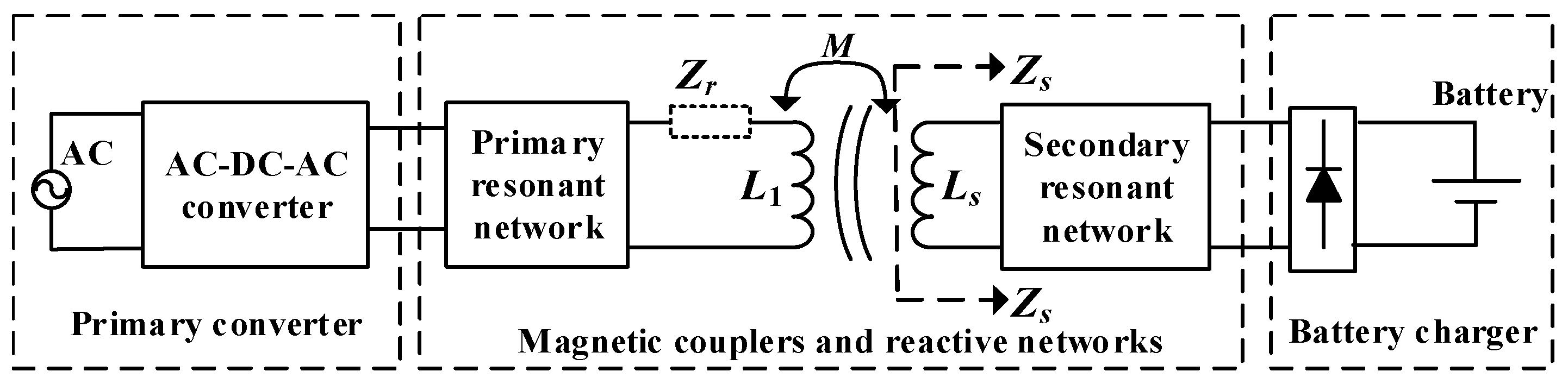
2.1. Fundamentals of WPT System

A WPT system typically has two coils at its heart that exchange energy from the transmitter to the receiver using high frequency magnetic links. Coils are compensated to improve power transfer efficiency. Primary compensation circuit boosts and filters the transmitter coil current, allowing the inverter of a relatively low volt-ampere (VA) rating to drive a highly inductive coil. The secondary compensation coil enhances power transfer by boosting the voltage and/or current at the secondary side [22,23,24]. As shown in Figure 1, the primary side consists of a rectifier, an AC-DC-AC converter that transforms the power frequency alternating current (AC) to high frequency AC current to increase the magnetic field density and system power capacity. In the secondary side, a high frequency rectifier is used to rectify and transform the AC power provided by the secondary coil to a suitable direct current (DC) for typical DC loads. The secondary converter could be omitted for smaller size, particularly if the power could be regulated by primary side.
In Figure 1, M is the mutual inductance between the two coils; Zs is the input impedance of the secondary side. The reflected impedance Zr is drawn by the dashed line and can be solved as:
Z r = ( ω 2 M 2 ) / Z s
where ω is angular frequency of the system and its value is fixed. By assuming Zs is a purely constant resistance, it can be concluded from Equation (1) that M is the only variable influencing the reflected load as long as the parameters in the WPT system are properly designed.

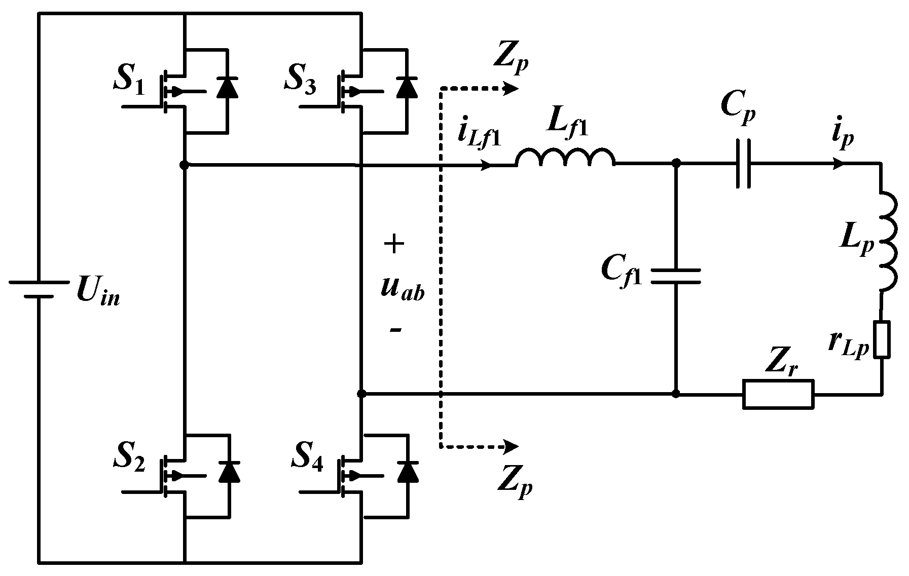
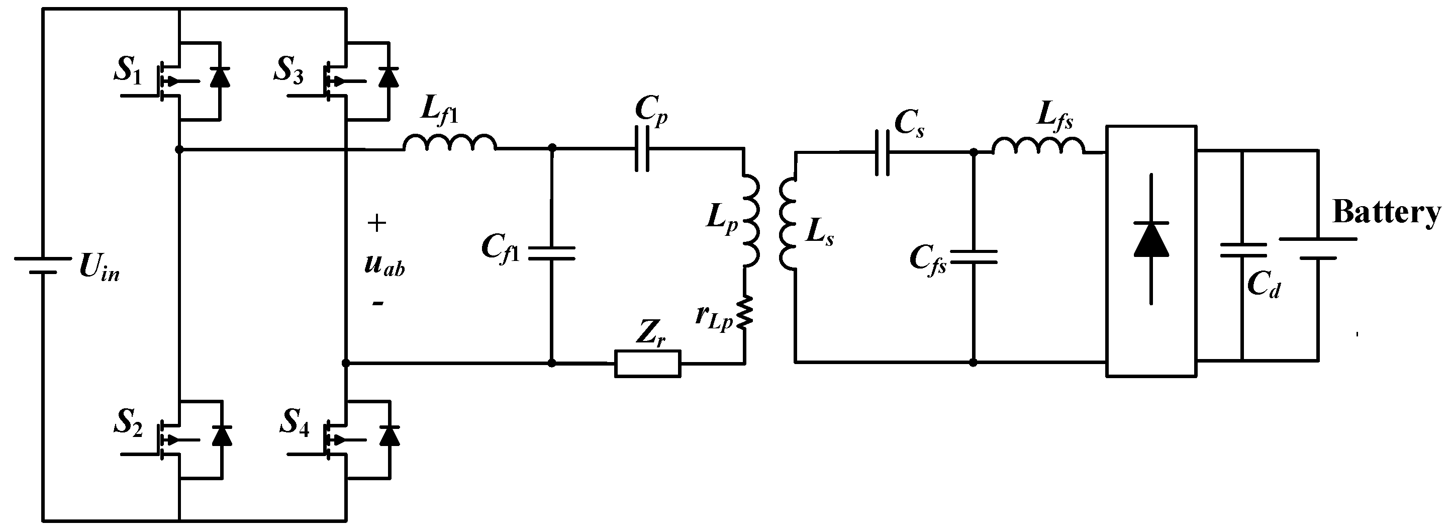
2.2. LCC Resonant Network in the Primary Side

In the dynamic wireless charging system, coils alignment is inevitable as the secondary coil moves with the online electric vehicles, resulting in the mutual inductance variation, which thus causes fluctuation of charging power. Besides, in order to maintain the system stability, a constant supply current for primary coil is necessary. Consequently, meticulous control and tuning of the inverter are needed to alleviate these obstacles. This, however, increases the control complexity and reduces operation reliability of system with basic series-series (SS) compensation topology. Later, a novel compensation topology, namely inductor-capacitor-capacitor (LCC) resonant network, was derived from the inductor-capacitor-inductor (LCL) topology and used in EV dynamic wireless charging systems [25,26]. It performs as a current source at resonance frequency [27,28] and is able to cancel the nonlinear effect of the rectifier diodes in the secondary side to achieve an exact unit power factor under a predetermined load condition [29]. Besides, it improves the lateral coils misalignment tolerance. The comparison study on SS and double-sided LCC compensation topologies [30] revealed that the double-sided LCC compensation topology is less sensitive to mistuning caused by the coils misalignment. Besides, both the voltage and current stresses on the series compensated capacitors and the main coils of the double-sided LCC compensation topology are smaller than those of the SS compensation topology. Thus, the LCC network is selected in this paper. A typical LCC topology in the primary side is shown in Figure 2. A voltage-fed, full-bridge converter is composed by Metal-Oxide-Semiconductor Field-Effect Transistors (MOSFETs) S1S4. Cf1 is the compensating capacitor for freewheeling inductance Lf1; Cp partly compensates primary coil Lp; rLp is the internal resistance of Lp; Zp is the output impedance of the inverter; Uin is the input DC voltage; uab and iLf1 are the output voltage and current of the inverter, respectively; ip is high-frequency current in the primary coil.
Assuming that the parasitic resistors in Lf1, Cf1, and Cp are ignored, the circuit parameters are designed by the following equations to achieve a constant resonant frequency for the topology.
{ L f 1 C f 1 = 1 / ω 0 2 ( L p L f 1 ) C p = 1 / ω 0 2
where ω0 is the resonant frequency. As soon as the system operates at the resonant frequency, Zp could be calculated based on impedance analysis as
Z p = L f 1 C f 1 ( Z r + r L p )
Zr will decrease to zero if the two coils are totally decoupled while Zp will be in the high impedance state, which is very different from primary series compensation topology. Similarly, the input current of the primary resonant network iLf1 can be solved as
i L f 1 = u a b C f 1 ( Z r + r L p ) / L f 1
From Equations (1) and (4), the input power of the resonant network Pin could be calculated as
P i n = u a b 2 C f 1 ( ω 2 M 2 + r L p Z s ) Z s L f 1
In the dynamic wireless charging system, M varies with the coils misalignment. In Equation (5), rLp, Cf1, Lf1, and Zs are seen as constant. Thus, Pin increases monotonically with M as soon as the uab is fixed. With the EV moving, the injected power could be regulated automatically only based on two coils’ coupled coefficient. This automatic power regulation characteristic in LCC topology is a natural fit for a dynamic wireless charging system.
The root mean square (RMS) of the high-frequency current in the primary coil ip could also be solved as
i p = u a b / ω L f 1
The total loss on primary pads’ parasitic resistors is
P l t o t a l = n u a b 2 r L p ω 2 L f 1 2
where n is the number of primary pads and Pl−total is the power loss on the parasitic resistor.
Equation (6) shows that in LCC resonant network, the primary pad current is independent of load or coupling condition. This characteristic is preferred in a stationary wireless charging system. However, in a dynamic wireless power transfer system, it will induce significant losses and EMI issues when the two coils are decoupled. For example, if the charging road has hundreds of meters extension, dozens of primary pads will be excited simultaneously, and thus the total loss on primary pads will be unacceptable as shown in Equation (7). Consequently, the selective switching control of primary pads is essential in a pads array dynamic wireless charging system. The corresponding switching control strategy and position detection method will be discussed in Section 3 and Section 4, respectively.
To verify the theory analysis, an inverter with LCC resonant network was set up in PLECS software (version 3.5.5, Plexim, Zurich, Switzerland) to simulate dynamic changing of the system. The results are shown in Figure 3, and the components’ parameters are noted below the figure.
Figure 3 simulated the process of an EV passing one specific primary pad within 50 ms. It is very clear that with the EV moving, the variation tendency of three curves, M, Zr, and Pin, are completely consistent. Because of over coupled [31], M does not reach the maximum value when the two coils are totally aligned. If two coils overlap very little, the magnetic flux generated by them are added destructively and the negative inductance appears during initial and final periods [32]. The RMS of ip is independent of any variation, which always keeps a constant. The simulation results verified that the Pin is monotonically increase with M.

3. Multiple Legs Inverter for Dynamic WPT System

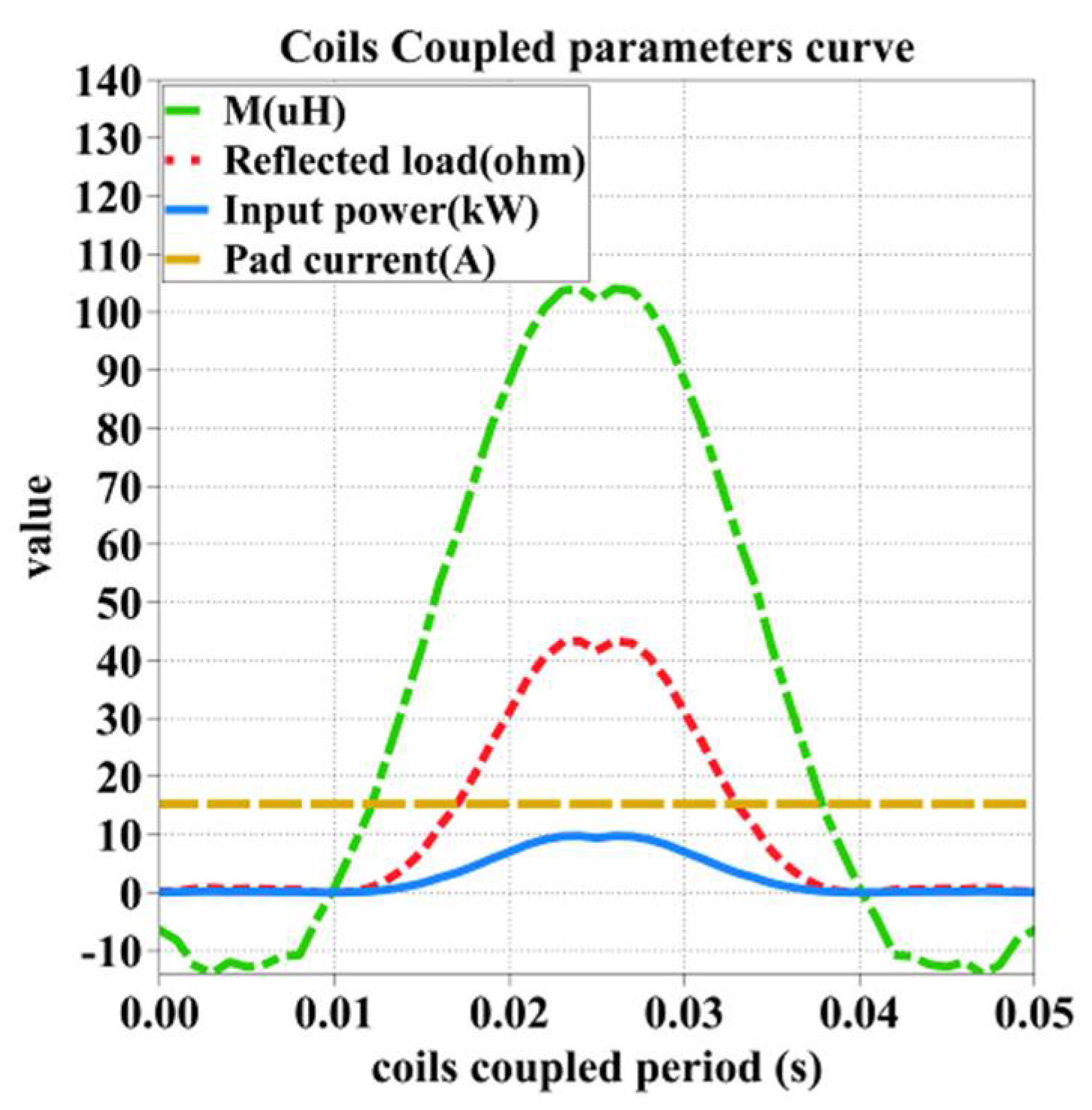
3.1. Characteristic of the Dynamic WPT System

As mentioned in Section 2, the constant current in each primary pad needs to be eliminated or significantly reduced when the two coils are decoupled. Thus, selective exciting control should be added into the pad array dynamic WPT system. For a conventional dynamic WPT system, one independent converter is designed only for one primary pad, and there are two working modes for each primary converter, namely charging mode and stand-by mode. When the two coils are coupled or partly coupled, the corresponding primary pad will be excited, and the converter is operating in the charging mode. After the EV passed the pad, the two coils are decoupled, in which case the constant pad current should be eliminated or reduced to a tiny value, and the corresponding converter is operating in stand-by mode. In general, for the dynamic charging primary converter, most of time, the system is operating in stand-by mode because the EV’s speed is so fast that it will take only tens of milliseconds to pass one primary pad. On the other hand, for a distance of dynamic wireless charging road, the total system power capability is the sum of all the primary converters along the charging road, however, there is only one converter is working at a time during the charging process. Therefore, the system’s real output power will be much smaller than its power capability, in which case most of the converters are idle and most of the power capability is wasted. Thus, the scheme as one primary converter for per pad in conventional dynamic pads array WPT system is uneconomical.

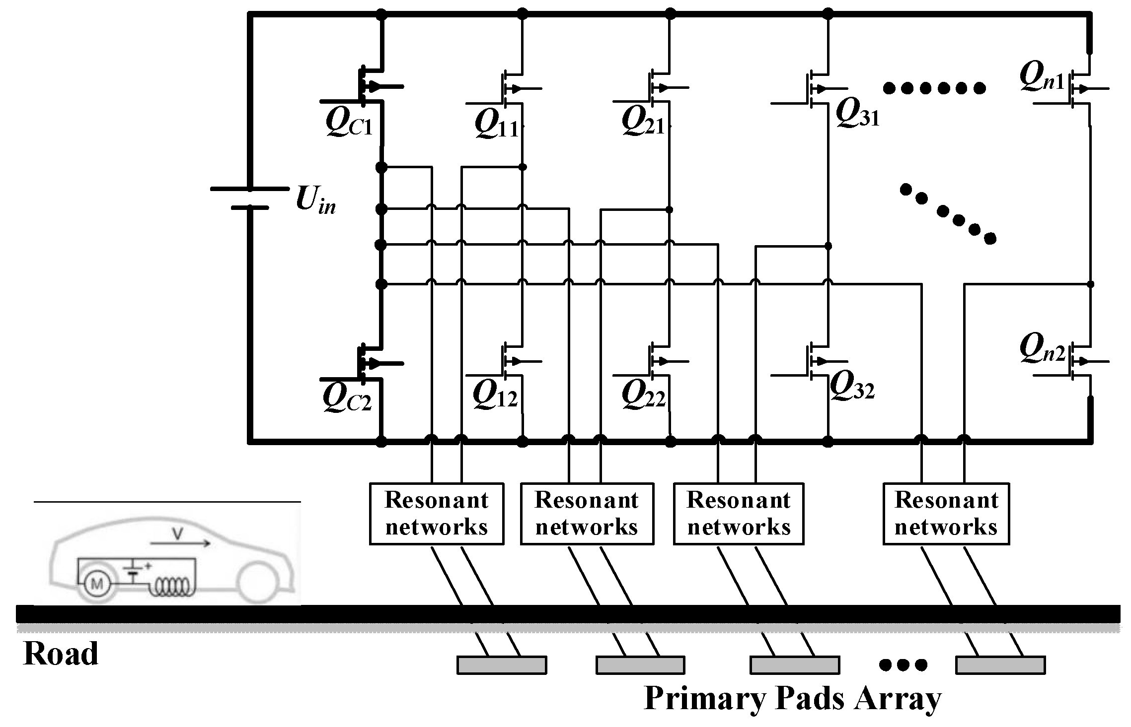
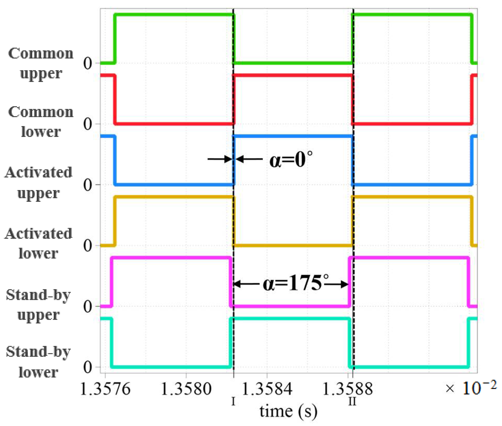
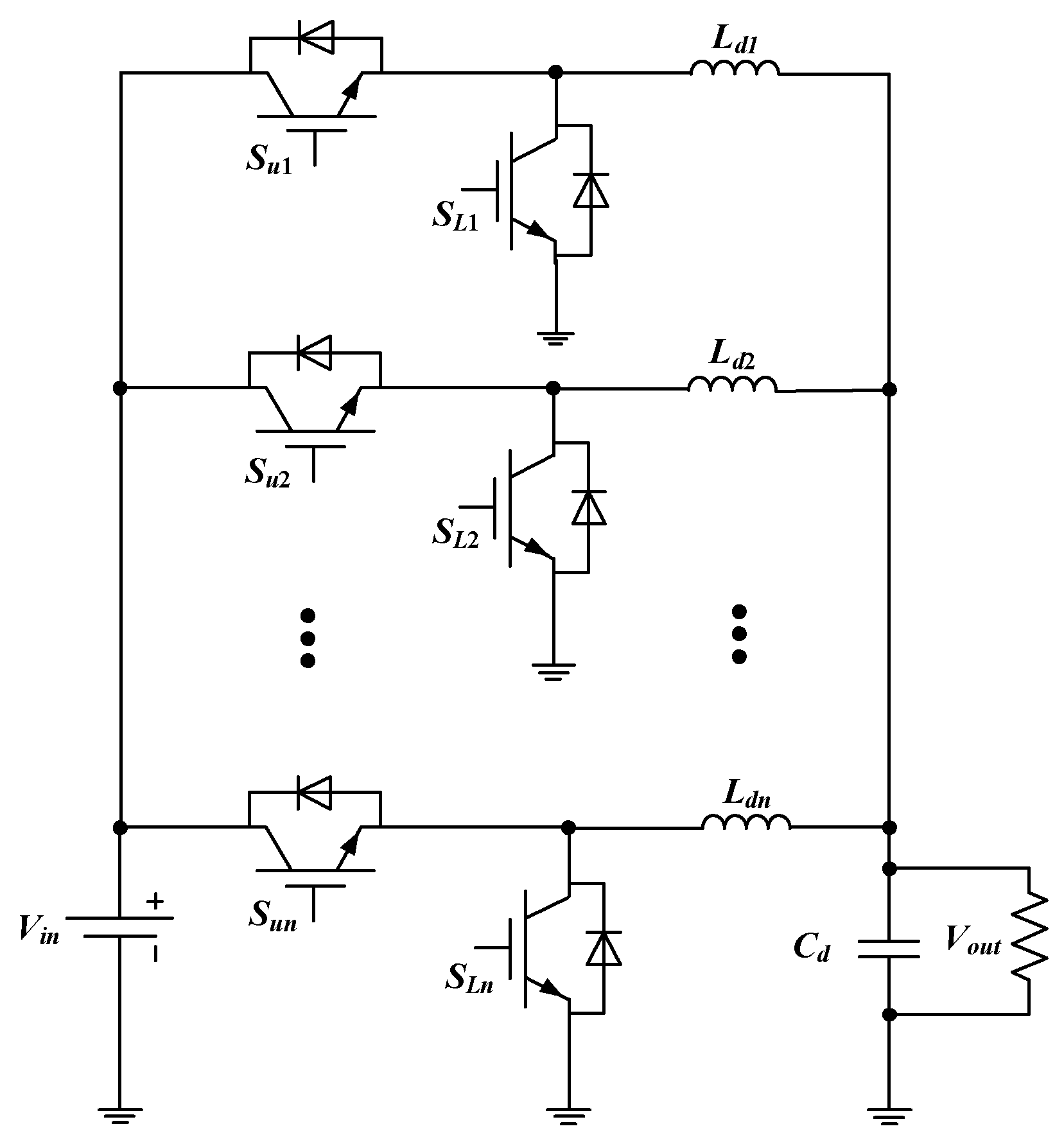
3.2. The Multiple Legs Inverter for Dynamic WPT System

As mentioned in Section 2, the power injected into LCC resonant network increases monotonically with M automatically, and different from primary series compensation topology, the input impedance in LCC topology is so high that it could be seemed as open circuit when the two coils are decoupled. Consequently, a multiple legs inverter is proposed in this paper in order to reduce the hardware cost and limit the constant currents in primary pads. The detail of the proposed circuit is shown in Figure 4, where one common leg and n selectable legs compose the novel voltage-feed full bridge inverter in primary side. QC1 and QC2 are upper and lower MOSFETs in the common leg respectively; upper MOSFETs Q11 to Qn1 and lower MOSFETs Q12 to Qn2 compose n selectable legs. Correspondingly, n LCC resonant networks are connected between the common leg and selectable legs respectively. The sequence numbers of each resonant network is same as the first subscript of the MOSFETs in selectable legs.
Similar with H bridge inverter, the driving signals for upper MOSFET and lower MOSFET in each leg are complementary. Due to the injected power increases monotonically with M, the selectable legs with their resonant networks are independent of each other. Phase shift full bridge (PSFB) control is adopted to limit the constant primary pad current amplitude. There are two operating modes in the multiple legs inverter. At the initial time, the two coils are decoupled and the inverter is operating in stand-by mode, in which case the current in each primary pad is limited, so there is almost no power flow into the resonant networks. As soon as the EV is approaching and partly coupled with the first primary pad, the first selectable leg will increase its phase shift angle rapidly until the desirable power flows into the EV battery, while other selectable legs will maintain their phase shift angle value. At this period, the powered selectable leg is working at charging mode and other selectable legs are working at stand-by mode. When the EV passed the powered pad, the first selectable leg will decrease its phase shift angle back to initial value and operate at stand-by mode. The second selectable leg will wait for startup signal and ready to be powered. With the EV moving, the selectable legs will be powered and switching the operating modes in sequence. By activating the primary pad successively, the proposed multiple legs inverter provides enough charging power to the battery and significantly reduces the power loss.
The driving signals for two operating modes are shown in Figure 5, where two driving signal waveforms for upper and lower MOSFETs in common legs, activated selectable legs, and stand-by selectable legs are complementary, respectively. In the charging mode, the phase shift angle between the powered selectable leg and the common leg is small so that the desired power could flow into the activated primary pad. In stand-by mode, the phase shift angle between the unpowered selectable leg and the common leg is large so that only tiny current is allowed to flow into the stand-by primary pads. The phase shift angles in different operating modes are labeled by dash line and indicated in the figure. It is worth mentioning that the phase shift angle for stand-by mode should not be set to 180 degree, and the reason will be discussed in Section 4. In Figure 5, the phase shift angle in the charging mode is set to 0 degrees, and that in stand-by mode is set to 175 degrees.

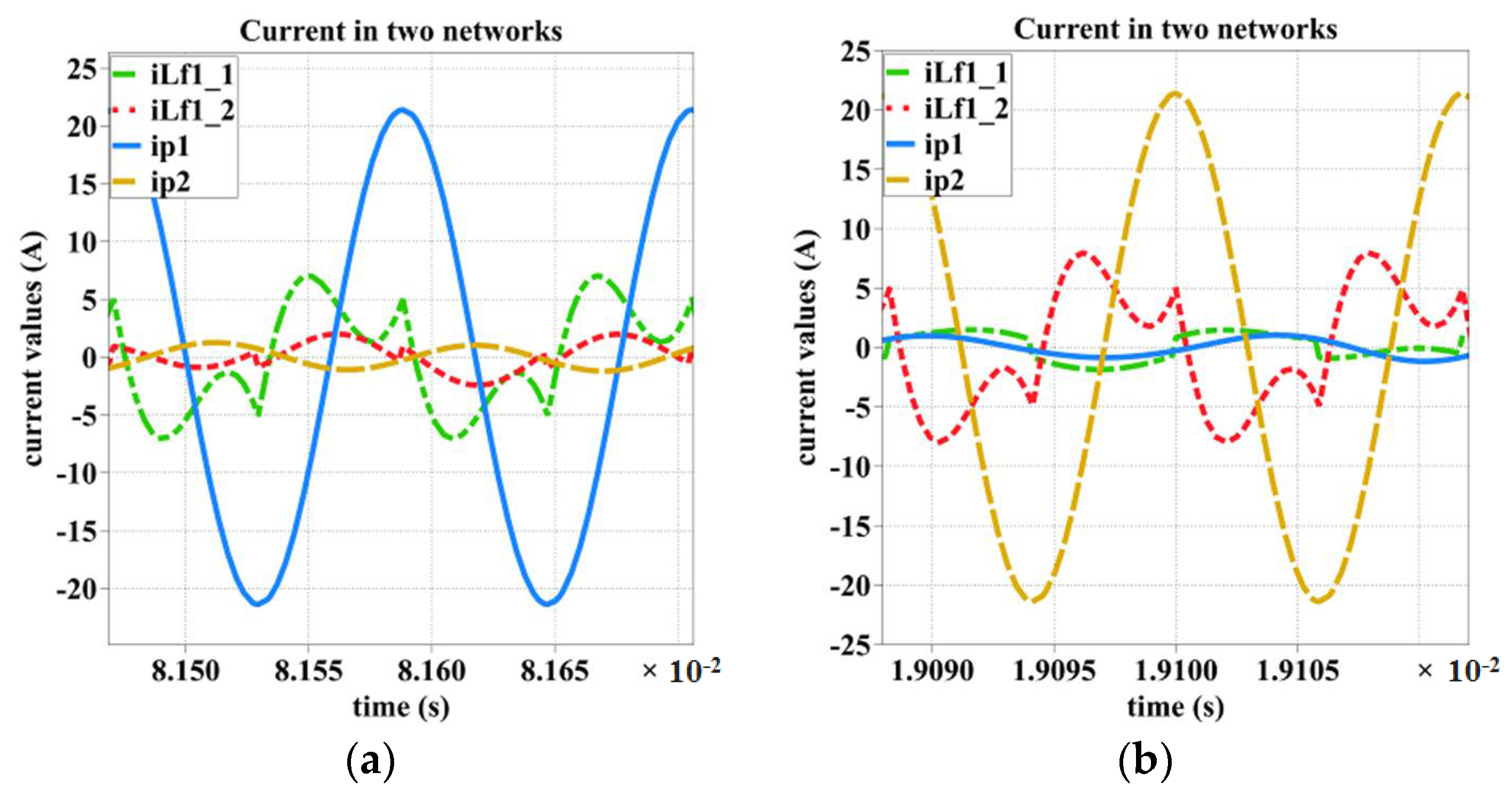
3.3. Simulation Verification

To verify the theoretical analysis on a multiple legs inverter, two identical adjacent LCC resonant networks with primary pads are selected to monitor the current variation. The simulation parameters are identical with the values below Figure 3. The simulation results are shown in Figure 6, where iLf1_1 and iLf1_2 are the input currents of two adjacent LCC resonant networks, respectively, ip1 and ip2 are primary pad currents of two networks. The phase shift angle for stand-by mode is set to 175 degrees.
It can be seen that when the secondary coil is aligned with the first primary pad, the phase shift angle in the first selectable leg is 0 degree to maximize the charging power, so the first selectable leg is operating at charging mode, in which case the RMS of ip1 is 15.2 A, and the RMS of the first-order harmonic of iLf1_1 is 4.1 A. Meanwhile, the second primary pad is decoupled, so the phase shift angle in the second selectable leg is 175 degree and it operates in stand-by mode, in which case the RMS of ip2 is only 0.8 A and the RMS of the first-order harmonic of iLf1_2 is 0.7 A. The corresponding current waveforms are shown in Figure 6a. With the EV moving, the secondary coil passed the first primary pad and aligned with second primary pad. Contrary to the previous state, the first selectable leg is switched to stand-by mode while the second one is switched to the charging mode. The current waveforms are shown in Figure 6b, which almost resembles Figure 6a. The simulation results proved the theory analysis that each selectable leg in the proposed multiple legs inverter could regulate the injected power and pads current independently, and the total power loss could be significantly reduced with proper control.
Compared to conventional WPT system with an independent inverter for each single primary pad, the proposed circuit can share only one central controller board. Because all the power flows through the common leg and distributed automatically among selectable legs, at least half of semiconductors and isolated gate drivers can be saved. Therefore, the multiple legs inverter can significantly reduce the converter cost in a dynamic wireless charging system. The hardware cost comparison will be discussed in Section 6.

4. Reflected Load Identification for LCC Topology

As analyzed in Section 3, the selectable legs should be powered selectively as soon as the coils are coupled. Therefore, the advantage of proposed inverter relies on accurate position detection. Otherwise, the transferred power will be significantly reduced and result in charging failure. As aforementioned, most of the existing position detection methods cannot perform well in high speed dynamic WPT system. As shown in Figure 3, the reflected load value could indicate the two coils coupling condition, therefore, it is feasible to detect the EV’s position via identifying reflected load. In this section, a novel reflected load identification method will be proposed for position detection and for system injected power regulation.

4.1. Principle of the Identification Method

Based on Equations (4) and (6), we can get
Z r = i L f 1 ω i p C f 1 r L p
In Equation (8), because ω, Cf1, and rLp can be considered as fixed values, as soon as the RMS values of iLf1 and ip are measured, the reflected load value can be identified. It is clear that only iLf1 and ip can influence the identification results rather than inverter input voltage uab, thus, only a small uab is needed to maintain the minimum iLf1 and ip that make sure both of them could be measured by current sensors. This is the reason that in the proposed multiple legs inverter, the maximum phase shift angle for each selectable leg should not be 180 degree as shown in Figure 5.
As shown in Figure 3, the two coils’ mutual inductance, which can indicate the EV’s position, increases monotonically with the reflected load. Therefore, the proposed reflected load identification method could be used to detect EV’s position. For each selectable leg in multiple legs inverter, two current sensors will be adopted to measure iLf1 and ip, and the central controller will calculate the reflected load value in real time. As the EV approaching the specific primary pad, the calculated reflected load increases sharply, then the corresponding selectable leg will be switched to charging mode immediately. As soon as the EV passed through, the calculated reflected load will decrease and the corresponding leg will be switched back to stand-by mode. Thus, the multiple legs inverter is able to selectively activate the primary pad based on the reflected load identification results.
Besides the position detection, the proposed identification method can be further applied for injected power regulation. As mentioned in Section 1, the general DSRC device cannot be applied to dynamic WPT system and the secondary data cannot be transmitted rapidly to primary side. Therefore, the injected power and output power are regulated independently in the primary side and the secondary side, which means that an extra costly and bulky DC-DC converter should be added in secondary side. However, the identification method could provide the accurate reflected load value in real time. Based on energy conservation law, it is feasible to regulate the injected power only at the primary side to manage the charging power. The power regulation based on reflected load identification method will be presented in Section 5.
Another advantage of the proposed identification method is that it can be used for system protection. For a conventional dynamic WPT system without bi-directional data transmission, any malfunctions in the secondary side will induce circuit fault at the primary side, even though the secondary side could be perfect protected. According to the proposed identification method, the load condition can be monitored in real time, and thus any fault in the secondary side will be timely reflected on the identification result. Then, the primary controller will estimate the situation and decide whether the injected energy needs to be cut off. The details will be presented in the simulation results at the end of this section.
It is worth mentioning that the accuracy of the identification result highly relies on the high precision of the current sensor. To the LCC resonant network, the pad current ip is a perfect sinusoidal wave in any condition. However, as shown in Figure 5, numerous higher order harmonics are combined in iLf1 and distort the current waveform, especially when the phase shift angle is large. In order to solve this issue, the true RMS chips will be used to obtain the accurate first-order harmonic value.

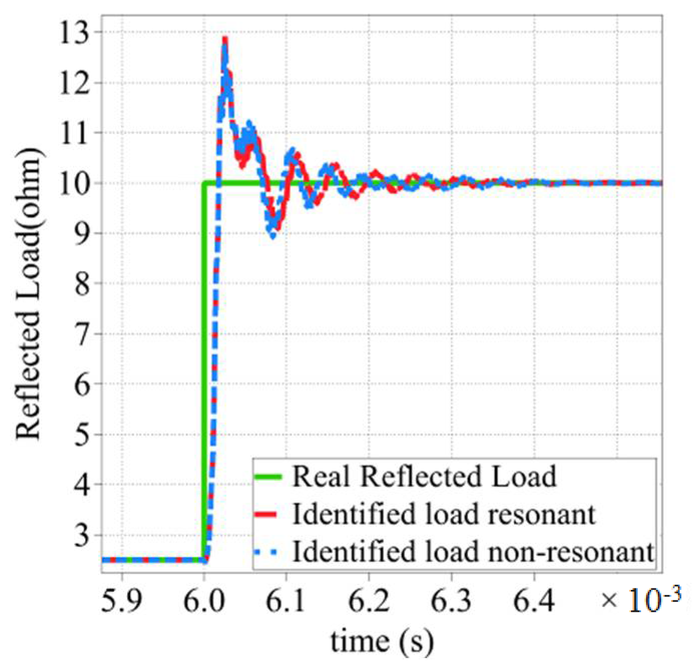
4.2. Simulation Verification

A simulation model was set up in PLECS software to verify the performance of the proposed reflected identification method. The model parameters are identical with the values below Figure 3. The simulation results are shown in Figure 7.
In Figure 7, the current RMS is sampled 50 times in each switching period. In the simulation, the reflected load is switched from 2.5 ohm to 10 ohm (load variation rate is up to 400%) at 6 ms, which is represented by the green solid curve. The blue dash line and red dash line are the identified reflected load curves when the system operates at resonant and non-resonant conditions, respectively. From the simulation results, it can be seen that even though the primary pad inductance changed from 300 μH to 275 μH, in which case the system operates at non-resonant condition, it has no influence on the identification result. The response time of the load identification is only about 200 μs, which is much faster than the conventional communication technology. According to the simulation results, it can be concluded that the proposed identification method has a high frequency robustness, fast response time and high identification precision, meeting the requirements of semiconductors protection and injected power control.

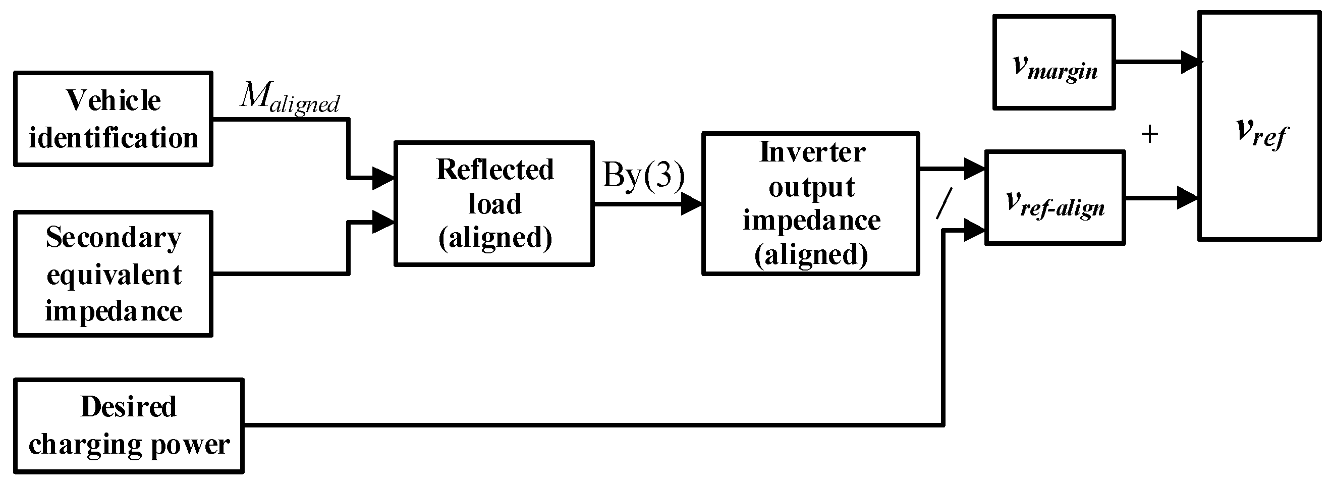
5. Power Control for the Proposed System

The dynamic wireless charging system, as a kind of public infrastructure, should meet the charging requirements of different vehicles, such as different battery charging power, different height of secondary coil setup. Aiming at this issue, a controller is needed to regulate the output voltage in a wide range. Even though the injected power could be solely regulated by PSFB, a DC–DC buck converter is also desired for requirements of higher efficiency, precision, and response. For example, the parasitic resistor loss of primary pads and the electromagnetic radiation can be significantly reduced via changing the phase shift angle values, which reduces the primary pad current. However, the undesirable switching loss and electromagnetic radiation also exists even when the selectable legs are operating in stand-by mode. In addition, there are some uncertain situations in practice, such as the desired charging rates, which depends on driver’s willing and battery state of charge (SOC) values in real time, the inevitable lateral misalignment, and so on. All of these practical issues can significantly increase the difficulty of the power regulation. Thus, in this section, a two-stages power regulation strategy is adopted, in which a fuzzy control buck DC-DC converter is used for coarse power regulation before vehicles covering the first primary pad and PSFB control is used for accurate output power regulation after vehicles covering the first primary pad. It is worth mentioning that as the DC-DC converter coarsely regulate the power before vehicles charging, it would not lead to additional delay for load identification and dynamic response of system control.

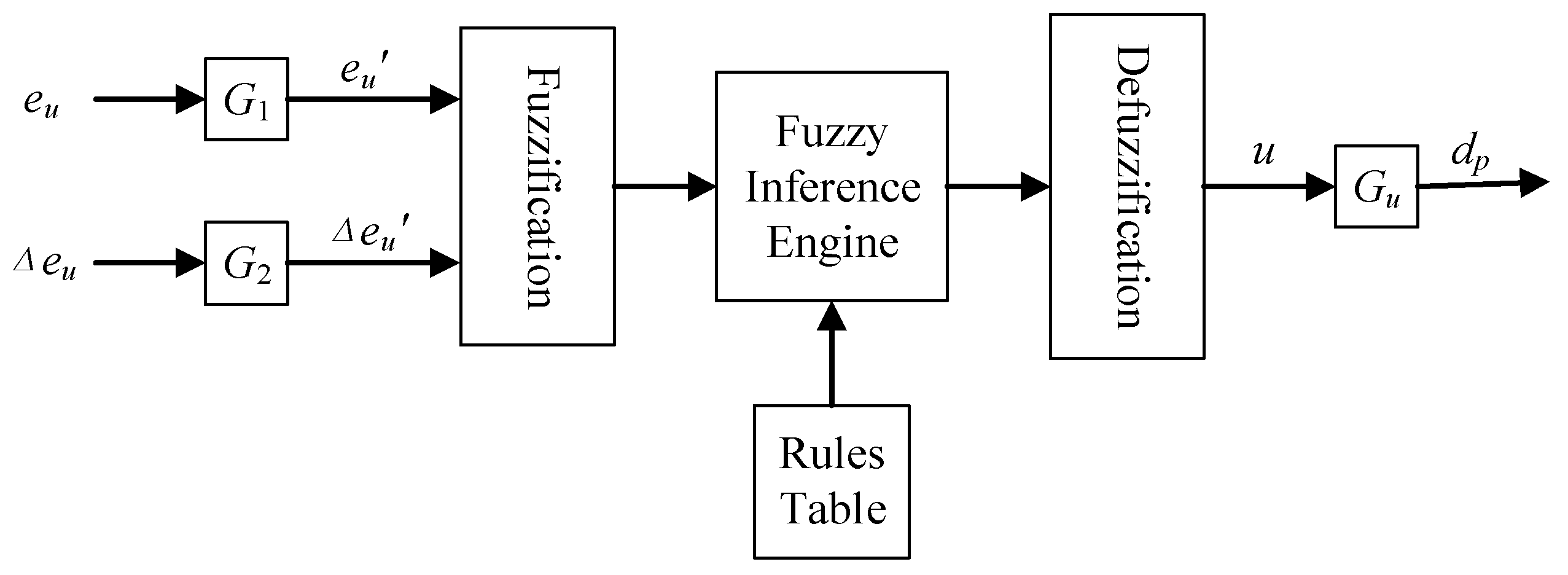
5.1. Design of Fuzzy Control DC-DC Converter

To reduce the switching loss and the output voltage ripple [33], a multiphase interleaved soft-switching synchronous buck converter is selected as the DC-DC converter in the primary side, which is shown in Figure 8, where each switching leg consists of two Insulated Gate Bipolar Transistors (IGBTs). Compared with other buck converters, the interleaved synchronous buck converter has the merits of high voltage conversion ratio, wide voltage regulation range, and low switch voltage stress, thus reduced switching losses [34,35]. A gate signal complimentary control scheme is used here in order to turn on the originally non-active switch and to divert the current into the anti-paralleled diode of the active switch. In this way, the main switch can be turned on under zero voltage conditions. The soft-switching operation can be considered as a zero-voltage resonant transition (ZVRT).
In Figure 8, Su1 to Sun are the upper IGBTs of each phase. Correspondingly, SL1 to SLn are the lower IGBTs of each phase. Ld1 to Ldn are the buck inductors and Cd is the common output filter. Vin and Vout are the input voltage and output voltage respectively. Each sub-buck can operate independently, and the phase shift between the adjacent sub-bucks is 180/n, where n is the number of the sub-buck converters.
For high speed EV, it will take several seconds to pass a short distance wireless charging road. Thus, the battery SOC can be considered as constant during this period. As a public EV charger, all the EV models can be charged via the proposed dynamic WPT system. However, the charging voltage and the charging current for different EV batteries are totally different. Even to the same batteries, the desired charging power is depend on driver’s willing which is totally uncertain in real time. In addition, as shown in Figure 3, the reflected load fluctuates remarkably due to the misalignment as the EV passing each primary pad. For the time varying and model uncertain system, it is difficult to set up a precise converter model for power regulation. Thus, the fuzzy control, which does not need an exact mathematical model, is introduced for the proposed DC-DC converter. Fuzzy control is a nonlinear controller, and it can regulate the power in variant supply voltage and variant load condition [36]. Besides, it performs better in terms of control accuracy and dynamic response as compared to linear proportional-integral-derivative (PID) controller. The block diagram of the designed fuzzy controller is shown in Figure 9.
From Figure 9, it can be seen that the fuzzy controller consists of six major parts, i.e., input scaling factor (G1 and G2), fuzzification, fuzzy inference engine, rules table, defuzzification and output denormalization factor Gu. The inputs of the fuzzy controller are defined as the error of output voltage eu(k) and the change of error Δeu(k).
e u ( k ) = v r e f v o u t ( k )
Δ e u ( k ) = e u ( k ) e u ( k 1 )
where vout(k) is the output voltage at the kth sampling step and vref is the reference voltage. After scaling, the actual inputs of the fuzzy system are the scaled version of voltage error eu′(k) and the change of error Δeu′(k).
e u ( k ) = G 1 e u ( k )
Δ e u ( k ) = G 2 Δ e u ( k )
The actual output of the fuzzy controller is the proportional part of the duty cycle dP.
d p = G u u
Five fuzzy levels are defined for eu′(k) and Δeu′(k), including NB = Negative Big, NS = Negative Small, ZE = Zero, PS = Positive Small, and PB = Positive Big. Table 1 shows the fuzzy control rules.
To obtain the battery information in advance, only one wireless communication device will be used for each primary converter. When the EV approaches the dynamic wireless charging road, the secondary information will be transferred to primary side in advance via WiFi device, including the desired charging power, equivalent impedance of the secondary side and the vehicle model identification number. Among them, the vehicle model identification number indicates the mutual inductance value when the two coils are aligned. As soon as the data was transmitted, the ideal DC-DC converter reference output voltage vref–align will be obtained by (3). In consideration of the lateral misalignment, a voltage margin vmargin should be added into the reference voltage, then the real DC-DC converter reference voltage vref(k) should be
v r e f = v r e f a l g i n + v m a r g i n
During the whole charging process, vref is fixed. The data transfer and calculation process is shown in Figure 10.
The proposed controller is featured as (1) the buck output voltage regulation process should be finished before the two coils are first coupled, (2) during the charging process, the output voltage of the buck keeps constant, (3) after the last coupled, the duty cycle of the buck converter is reduced down to zero, and (4) the whole system will wait for the next startup signal from WiFi for charging another EV.

5.2. PSFB Control for Multiple Legs Inverter

Because the vmargin is added in the DC-DC converter, the output power should be larger than the desired one when the two coils are aligned. Thus, the PSFB control is adopted for precise power regulation. The range of the output voltage regulation by PSFB is much narrower than DC-DC buck converter. Therefore, PID control could be applied in this situation. The system modeling for a similar resonant network with PSFB control was clearly presented in [37], so we do not repeat the modeling process herein but only discuss the control process.
The output power regulation process, the variation of the phase shift angle, and the primary pad current are shown in Figure 11. At the initial moment t0, the two coils are decoupled, so the corresponding selectable leg operates at stand-by mode where only tiny power flows into the resonant network to ensure that iLf and ip are measureable. As soon as the two coils begin to be coupled at t1, sudden change of the reflected load is detected, then the phase shift angle will be decreased to zero rapidly in order to activate the corresponding primary pad. However, due to large misalignment, the output power could not meet the system’s requirement. With the two coils aligned gradually, the output power will increase, and the real output power will be equal to the goal output power at t2. From then on, the phase shift angle will increase to limit the output power and maintain it to a constant value. With the increasing of the phase shift angle, the primary pad current will decrease gradually. After the two coils are totally aligned at t3, the misalignment will increase gradually. In order to maintain the output power, the phase shift angle will decrease gradually and go back to zero at t4. During this period, the primary pad current will be increased. Then, the output power cannot be maintained, and with the EV moving, it will be decreased to a tiny value at t5. At that time, no reflected load is identified, and the corresponding selectable leg will be set back to stand-by mode.
In Figure 11, based on the law of the energy conservation, the real output power can be calculated as
P o u t = i p 2 Z r r s l o s s
where ip can be measured and Zr can be identified via Equation (8) in real time, and rs-loss is the secondary coil loss, which can be measured in advance.

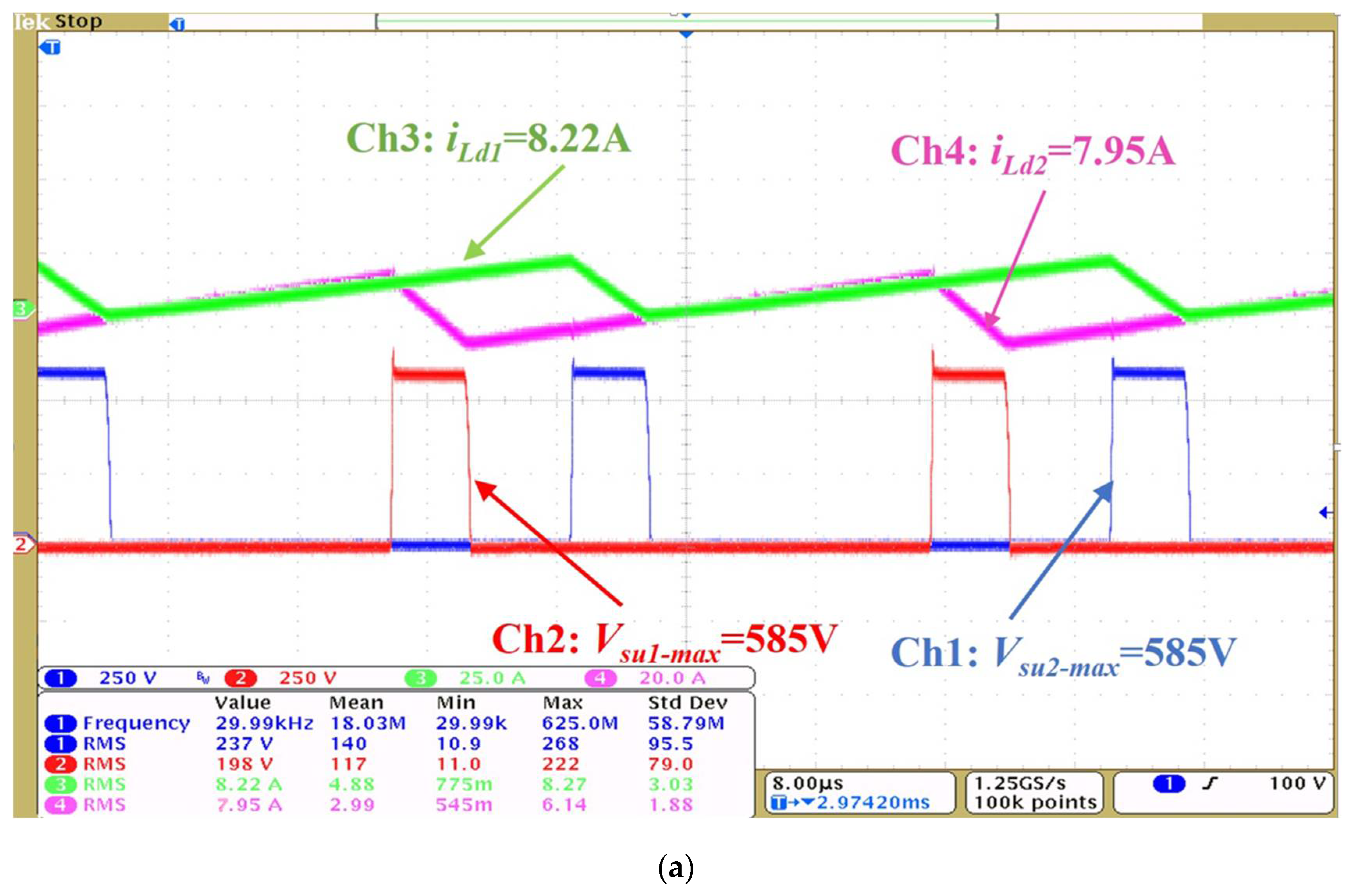
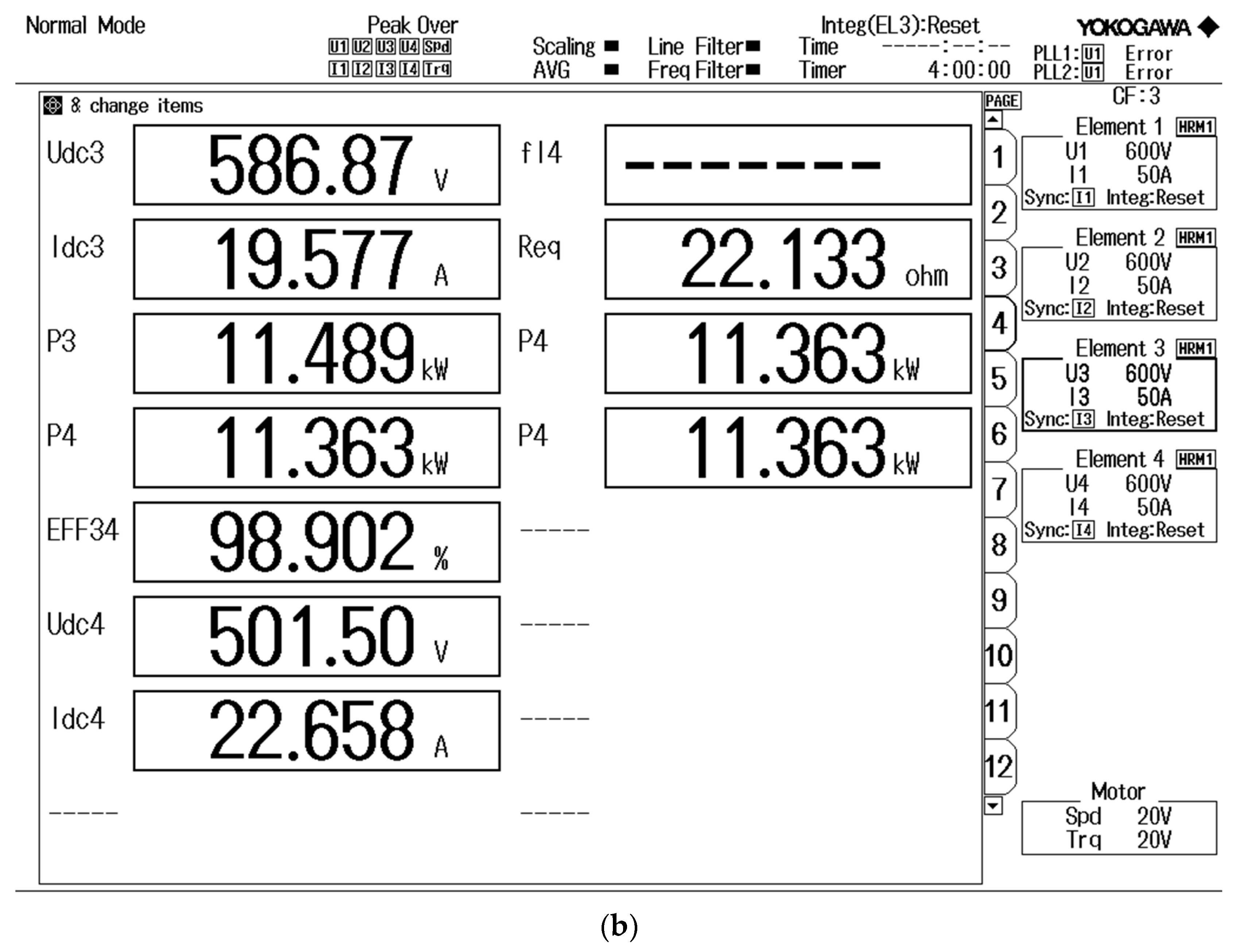
6. Experimental Verification and Analysis

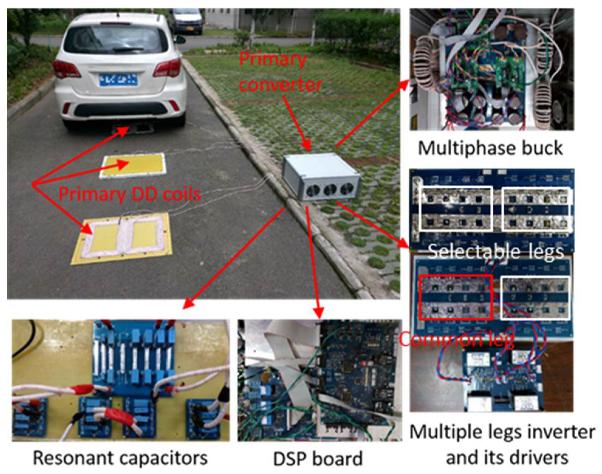
6.1. Experimental Verification

To validate the proposed circuit and the above analysis, a prototype of a dynamic WPT charging system was established. Due to the components are symmetrical, double LCC resonant networks are selected in order to simplify the parameters design process. The double LCC resonant network is shown in Figure 12. The experimental setup is shown in Figure 13, and the specifications of the prototype are listed in Table 2.
In Figure 13, double D (DD) coils [38] are adopted both in the primary side and the secondary side to improve the misalignment tolerance. Three primary DD pads are paralleled side by side to compose the primary pads array which is activated by a sole multiple legs inverter. The distance between the two adjacent coils is 1 m. The components’ parameters in three primary LCC resonant networks are approximately identical with each other, as shown in Table 3. The multiphase buck contains three phases sub-buck circuit, and the phase angle between each two phases is 120 degree.
In the prototype, double TMS320F28335 plus (Texas Instruments, Inc, Dallas, TX, USA) Complex Programmable Logic Device (CPLD) are adopted as the system’s central controller. For the multiple legs inverter, each leg, whether a common leg or selectable leg, is driven by one magnetic coupled gate driver ADUM3223 (Analog Devices, Norwood, MA, USA); Rohm SiC MOSFETs SCT2080KE (ROHM Co., Ltd., Kyoto, Japan) (1200 V, 40 A) are adopted as inverter switching for high voltage level and lower conduct loss. The compensated film capacitors in LCC resonant network are EPCOS MKP10 (EPCOS, München, Germany) whose loss angle is around 1.5‰ at 100 kHz. It is worth mentioning that the proposed multiple legs inverter can be implemented with a number of full bridge inverter boards. In the prototype developed in this paper, a four-leg inverter with one common leg and three selectable legs is needed to activate the three primary pads. Therefore, two full bridge inverter boards were used to implement the four-leg inverter, as shown in the Figure 13. Besides, each half-leg consists of several MOSFETs connected in parallel to meet the power requirement. For multiphase interleaved soft-switching synchronous, high-speed IGBTs Infineon IKW40N120H3 (Infineon Technologies, München, Germany) are applied, which exhibit extremely low switching losses. Two channels integrated IGBT driver boards TX-DA962A (Beijing LMY Electronics Co., Ltd., Beijing, China) are chosen to drive IGBTs in buck circuit.
Figure 14 shows the waveforms and power analysis results for the multiphase interleaved soft-switching synchronous buck. The duty cycle of each phase is fixed at 85%. The switching frequency is fixed at 30 kHz. From the upper part in Figure 14, the IGBT in each phase almost reaches soft switching, and the inductor current in each phase is almost identity. According to the power analyzer, the output power is about 11.4 kW, and the total efficiency is up to 98.9%.
Figure 15 shows the input voltage and current waveforms for two adjacent primary LCC resonant networks with different operating modes, in which case the first primary pad was decoupled and the second primary pad was partly coupled. To first primary resonant network, the PSFB control was working to limit the primary pad current. The RMS of the injected current is only 0.76 A which could be measured by current sensor precisely. It should be noted that due to the dead-time and clear observation, the phase shift angle was set to 155 degrees rather than 175 degrees. To the second resonant network, the two coils were partly coupled so that there is no phase shift angle between the common leg and the selectable leg. The input current of the second network is 15.8 A and the injected power is 5.6 kW. The experimental results indicated that the multiple legs inverter could perform well in the proposed scheme.
Figure 16 shows the real power regulation process for one primary resonant network. At the initial moment, the two coils were decoupled, so the corresponding resonant network was operating in stand-by mode, in which case the primary pad current ip was limited by a large phase shift angle. With the EV moving, as soon as the two coils started to be coupled, the reflected load was identified and the phase shift angle was decreased to zero quickly, thus the primary pad current was increased to steady state value immediately. When the two coils were almost aligned, the PSFB control began to work, and the primary pad current decreased due to the RMS value of uab decreasing. During this period, the system was operating in a constant output power condition. When the EV moved away, the two coils were decoupled, so the reflected load identification result was almost zero, and the phase shift angle in the corresponding selectable leg increased to a large value again, leading a tiny value of the primary pad current. With this, for one primary resonant network, the power control process was finished. The experimental results proved that the two stages power regulation method could perform well in the proposed system.

6.2. Cost Analysis

A cost comparison between conventional dynamic WPT system with an independent converter for each primary pad and the proposed system has been made. Assuming that there are 30 primary pads placed side by side along the 50 m charging road. The system parameters and the components’ part number were identical with the test prototype system, and the rate output power of each primary pad is 7.7 kW. The components’ unit price and quality demands for two different schemes are shown in Table 4. It should be noted that only the difference between these two schemes is presented herein.
It is assumed that the common power factor correction (PFC) and the input AC-DC converter could be shared in both of the schemes. To the conventional scheme: (1) 30 independent DC-DC and DC-AC converters are needed, and each inverter contains four MOSFETs and four isolated gate driver circuits; (2) 30 position detectors are needed to detect the EV’s position; (3) 30 speed sensors are used for measuring the EV’s speed to startup the system in advance to compensate the WiFi’s delay; (4) each primary converter needs one central control board and one electrical case, then the total cost is $31,100. To the proposed scheme: (1) only one DC-DC converter is needed, and the sole inverter includes one common leg and 30 selectable legs, which consume 62 MOSFETs and isolated gate drivers in total; (2) it needs more advanced central controller because more PWM ports are needed; (3) similarly, a larger electrical case is desirable; (4) thus, both of central control board and electrical case are more expensive than conventional ones, then the total cost of the proposed scheme is $6750. The comparison result shows that the proposed scheme can reduce the cost by 78% compared with the conventional system.

7. Conclusions

A novel multiple legs inverter and reflected load identification method are proposed for a dynamic wireless charging system of electric vehicles in this paper. The advantages of using a multiple legs inverter with a paralleled LCC resonant network include that all the sub-compensation networks can be activated by a single primary converter and the power between different networks can be distributed automatically only depending on the EV’s position, which significantly reduces the system hardware cost. To detect the EV’s position and control the system’s injected power precisely, a high-response and simple method for reflected load identification was proposed. The identification method can be used to activate the primary coils selectively for minimizing the electromagnetic inference and limiting the constant currents in the primary pads and can also provide the control reference to the power regulation circuit. A two-stage power regulation strategy combining the fuzzy control with PSFB control is adopted to stabilize the charging voltage. The efficiency of the proposed multiple legs inverter, the reflected load identification method, and the power regulation strategy are verified by a prototype with three primary DD coils and one secondary DD coil. Finally, the cost comparison results indicate that the proposed system can reduce the cost by 78% compared with the conventional system.
It is worth mentioning that the proposed multiple legs inverter is used to selectively activate one or more of the primary pads in a certain range, e.g., 30 m. Although we have practically assumed only a single pad is activated at any moment considering the vehicle size and the safe distance between two adjacent vehicles in this paper, the multiple legs inverter can activate more than one leg theoretically, in which case current through the common leg equals to the sum of that through the activated selectable legs. However, it is impossible for the multiple legs inverter to activate a large number of primary pads simultaneously, so the increasing cost and loss can be neglected. Power regulation in this case is more complicated. For example, if two vehicles with different battery power need to be charged simultaneously, the DC-DC converter will be regulated to meet the higher one, and the one with lower power requirement will be further controlled via the phase shift full bridge with a phase shift angle bigger than zero. Additionally, in the proposed method, the primary input voltage is rapidly and roughly regulated to a reasonable level before the electric vehicle entering the first pad. Then, as the vehicle enters the first pad, the phase shift full bridge control is responsible for accurately adjusting the input voltage of primary pad, and the fuzzy controller does not work anymore. Due to the experiment limitation, a prototype containing only one vehicle was developed in this paper, so only the phase shift full bridge controller worked during the dynamic wireless charging experiments. In the future work, we will focus on developing a prototype containing multiple loads to further assess the dynamic performance of the fuzzy controller and investigate the control strategy for multi-load with different charging requirements as well as investigating optimal coil topologies well suitable for dynamic and static wireless charging application simultaneously.

Author Contributions

Y.T. and S.Z. presented the original idea of the research and prepared the manuscript. Y.T. and D.L. performed the experiments together. The final manuscript was corrected by J.T. and S.Z.

Acknowledgments

This work was simultaneously supported by the Science and Technology Plan Project of Shenzhen (No. JCYJ20170412110241478).

Conflicts of Interest

The authors declare no conflict of interest.

References

  1. Düsterwald, H.G.; Günnewig, J.; Radtke, P. DRIVE-The future of automotive power: Fuel cells perspective. Fuel Cells 2007, 7, 183–189. [Google Scholar] [CrossRef]
  2. Tian, Y.; Chen, C.R.; Xia, B.Z.; Sun, W.; Xu, Z.H.; Zheng, W.W. An Adaptive Gain Nonlinear Observer for State of Charge Estimation of Lithium-Ion Batteries in Electric Vehicles. Energies 2014, 7, 5995–6012. [Google Scholar] [CrossRef]
  3. García-Vazquez, C.A.; Llorens-Iborra, F.; Fernandez-Ramírez, L.M.; Sanchez-Sainz, H.; Jurado, F. Comparative study of dynamic wireless charging of electric vehicles in motorway, highway and urban stretches. Energy 2017, 137, 42–57. [Google Scholar] [CrossRef]
  4. Rakhymbay, A.; Khamitov, A.; Bagheri, M.; Alimkhanuly, B.; Lu, M.; Phung, T. Precise Analysis on Mutual Inductance Variation in Dynamic Wireless Charging of Electric Vehicle. Energies 2018, 11, 624. [Google Scholar] [CrossRef]
  5. Jeong, S.; Jang, Y.J.; Kum, D. Economic analysis of the dynamic charging electric vehicle. IEEE Trans. Power Electron. 2015, 30, 6368–6377. [Google Scholar] [CrossRef]
  6. Suh, I.S.; Lee, M.; Kim, J.; Oh, S.T.; Won, J.P. Design and experimental analysis of an efficient HVAC (heating, ventilation, air-conditioning) system on an electric bus with dynamic on-road wireless charging. Energy 2015, 81, 262–273. [Google Scholar] [CrossRef]
  7. Yin, J.; Lin, D.; Lee, C.K.; Parisini, T.; Hui, S.Y. Front-end monitoring of multiple loads in wireless power transfer systems without wireless communication systems. IEEE Trans. Power Electron. 2016, 31, 2510–2517. [Google Scholar]
  8. Mai, R.K.; Li, H.C.; Liu, Y.R.; Zhou, K.Z.; Fu, L.; He, Z.Y. A Three-Phase Dynamic Wireless Charging System with Constant Output Voltage. Energies 2018, 11, 45. [Google Scholar] [CrossRef]
  9. Naberezhnykh, D.; Reed, N.; Ognissanto, F.; Theodoropoulos, T.; Bludszuweit, H. Operational requirements for dynamic wireless power transfer systems for electric vehicles. In Proceedings of the IEEE International Electric Vehicle Conference (IEVC), Florence, Italy, 17–19 December 2014; pp. 1–8. [Google Scholar]
  10. Marchukov, R.; Masotti, D.; Costanzo, A. Dynamic wireless power transfer by time-modulated arrays. In Proceedings of the IEEE Antennas and Propagation Society International Symposium (APS), Vancouver, BC, Canada, 19–24 July 2015; pp. 808–809. [Google Scholar]
  11. Sampath, J.P.K.; Vilathgamuwa, D.M.; Alphones, A. Efficiency enhancement for dynamic wireless power transfer system with segmented transmitter array. IEEE Trans. Transp. Electrification 2016, 2, 76–85. [Google Scholar] [CrossRef]
  12. Throngnumchai, K.; Hanamura, A.; Naruse, Y.; Takeda, K. Design and evaluation of a wireless power transfer system with road embedded transmitter coils for dynamic charging of electric vehicles. In Proceedings of the 27th World Electric Vehicle Symposium and Exhibition (EVS), Barcelona, Spain, 17–20 November 2013; pp. 1–10. [Google Scholar]
  13. Zhong, W.; Hui, S.Y.R. Auxiliary circuits for power flow control in multifrequency wireless power transfer systems with multiple receivers. IEEE Trans. Power Electron. 2015, 3, 5902–5910. [Google Scholar] [CrossRef]
  14. Vassis, D.; Kormentzas, G.; Rouskas, A.; Maglogiannis, I. The IEEE 802.11g Standard for High Data Rate WLANs. IEEE Netw. Mag. 2005, 19, 21–26. [Google Scholar] [CrossRef]
  15. Yoon, S.W.; Dang, T.S.; Lai, N.D.H.; Park, J.Y. Efficient Wi-Fi power amplifier LTCC module using a buck converter with a power inductor implemented in ferrite-filled PCB technology. IEEE Trans. Compon. Packag. Manuf. Technol. 2015, 5, 887–894. [Google Scholar] [CrossRef]
  16. Golsorkhi, M.; Lu, D.; Guerrero, J.A. GPS-based decentralized control method for islanded microgrids. IEEE Trans. Power Electron. 2017, 32, 1615–1625. [Google Scholar] [CrossRef]
  17. Kim, Y.J.; Ha, D.; Chappell, W.J.; Irazoqui, P.P. Selective wireless power transfer for smart power distribution in a miniature-sized multiple-receiver system. IEEE Trans. Ind. Electron. 2016, 63, 1853–1862. [Google Scholar] [CrossRef]
  18. Choi, B.H.; Thai, V.X.; Lee, E.S.; Kim, J.H.; Rim, C.T. Dipole-coil-based wide-range inductive power transfer systems for wireless sensors. IEEE Trans. Ind. Electron. 2016, 63, 3158–3167. [Google Scholar] [CrossRef]
  19. Abdolkhani, A.; Hu, A.P. Improved coupling design of contactless slipring for rotary applications. IEEE J. Emerg. Sel. Top. Power Electron. 2015, 3, 288–295. [Google Scholar] [CrossRef]
  20. Nagendra, G.R.; Covic, G.A.; Boys, J.T. Determining the physical size of inductive couplers for IPT EV systems. IEEE J. Emerg. Sel. Top. Power Electron. 2014, 2, 571–583. [Google Scholar] [CrossRef]
  21. Xiang, L.J.; Sun, Y.; Ye, Z.H.; Wang, Z.H.; Zhou, S.J. Combined primary coupler design and control for EV dynamic wireless charging system. In Proceedings of the 2016 IEEE PELS Workshop on Emerging Technologies: Wireless Power Transfer (WoW), Knoxville, TN, USA, 4–6 October 2016; pp. 174–179. [Google Scholar]
  22. Nagendra, G.R.; Boys, J.T.; Covic, G.A.; Riar, B.S.; Sondhi, A. Design of a double coupled IPT EV highway. In Proceedings of the 39th Annual Conference of the IEEE Industrial Electronics Society, Vienna, Austria, 10–13 November 2013; pp. 4606–4611. [Google Scholar]
  23. Choi, S.Y.; Huh, J.; Lee, W.Y.; Rim, C.T. Asymmetric coil sets for wireless stationary EV chargers with large lateral tolerance by dominant field analysis. IEEE Trans. Power Electron. 2014, 29, 6406–6420. [Google Scholar] [CrossRef]
  24. Ye, Z.H.; Sun, Y.; Dai, X.; Tang, C.S.; Wang, Z.H.; Su, Y.G. Energy efficiency analysis of u-coil wireless power transfer system. IEEE Trans. Power Electron. 2016, 31, 4809–4817. [Google Scholar] [CrossRef]
  25. Li, S.Q.; Li, W.H.; Deng, J.J.; Nguyen, T.D.; Mi, C.C. A double-sided LCC compensation network and its tuning method for wireless power transfer. IEEE Trans. Veh. Technol. 2015, 64, 2261–2273. [Google Scholar] [CrossRef]
  26. Zhu, Q.W.; Wang, L.F.; Guo, Y.J.; Liao, C.L.; Li, F. Applying LCC compensation network to dynamic wireless EV charging system. IEEE Trans. Ind. Electron. 2016, 63, 6557–6567. [Google Scholar] [CrossRef]
  27. Zhang, X.; Lai, Z.Y.; Xiong, R.; Li, Z.; Zhang, Z.L.; Song, L. Switching Device Dead Time Optimization of Resonant Double-Sided LCC Wireless Charging System for Electric Vehicles. Energies 2017, 10, 1772. [Google Scholar] [CrossRef]
  28. Deng, J.J.; Pang, B.; Shi, W.L.; Wang, Z.P. A new integration method with minimized extra coupling effects using inductor and capacitor series-parallel compensation for wireless EV charger. Appl. Energy 2017, 207, 405–416. [Google Scholar] [CrossRef]
  29. Miller, J.M.; Jones, P.T.; Li, J.M.; Onar, O.C. ORNL experience and challenges facing dynamic wireless power charging of EV’s. IEEE Circuits Syst. Mag. 2015, 15, 40–53. [Google Scholar] [CrossRef]
  30. Li, W.H.; Zhao, H.; Deng, J.J.; Li, S.Q.; Mi, C.C. Comparison study on SS and double-sided LCC compensation topologies for EV/PHEV wireless chargers. IEEE Trans. Veh. Technol. 2016, 65, 4429–4439. [Google Scholar] [CrossRef]
  31. Kim, Y.G.; Lim, Y.; Yun, S.; Nam, S. Mutual coupling analysis of antennas in layered media through equivalent sources for wireless power transfer. In Proceedings of the 2014 USNC-URSI Radio Science Meeting (Joint with AP-S Symposium) (USNC-URSI), Memphis, TN, USA, 6–11 July 2014; p. 115. [Google Scholar]
  32. Su, Y.P.; Liu, X.; Hui, S.Y.R. Mutual inductance calculation of movable planar coils on parallel surfaces. IEEE Trans. Power Electron. 2004, 24, 1115–1123. [Google Scholar] [CrossRef]
  33. Pevere, A.; Petrella, R.; Mi, C.C.; Zhou, S.J. Design of a high efficiency 22 kW wireless power transfer system for EVs fast contactless charging stations. In Proceedings of the 2014 IEEE International Electric Vehicle Conference, Florence, Italy, 17–19 December 2014; pp. 1–7. [Google Scholar]
  34. Muralidharan, G.P.; Bhaskarar, K. Interleaved Synchronous Buck Converter with High Conversion Ratio and Voltage Regulation. In Proceedings of the 2015 International Conference on Circuit, Power and Computing Technologies (ICCPCT), Nagercoil, India, 19–20 March 2015; p. 7159339. [Google Scholar]
  35. Debbou, M.; Colet, F. Interleaved DC/DC Charger for Wireless Power Transfer. In Proceedings of the 2017 IEEE International Conference on Industrial Technology (ICIT), Toronto, ON, Canada, 22–25 March 2017; pp. 1555–1560. [Google Scholar]
  36. Patil, B.U.; Jagtap, S.R. Adaptive Fuzzy Logic Controller for Buck Converter. In Proceedings of the 2015 International Conference on Computation of Power, Energy Information and Communication (ICCPEIC), Chennai, India, 22–23 April 2015; pp. 78–82. [Google Scholar]
  37. Hao, H.; Covic, G.A.; Boys, J.T. An approximate dynamic model of LCL-T-based inductive power transfer power supplies. IEEE Trans. Power Electron. 2014, 29, 5554–5567. [Google Scholar] [CrossRef]
  38. Budhia, M.; Boys, J.T.; Covic, G.A.; Huang, C.Y. Development of a single-sided flux magnetic coupler for electric vehicle IPT charging systems. IEEE Trans. Ind. Electron. 2013, 60, 318–328. [Google Scholar] [CrossRef]
Figure 1. Typical structure of the wireless power transfer (WPT) system.
Energies 11 01275 g001
Figure 2. Inductor-capacitor-capacitor (LCC) compensation network in the primary side.
Energies 11 01275 g002
Figure 3. Parameters varied with M (Lp = 300 μH, Lf1 = 50 μH, Zs = 71.3 ohm, Uin = 450 V, f = 85 kHz).
Energies 11 01275 g003
Figure 4. Multiple legs inverter for dynamic WPT system.
Energies 11 01275 g004
Figure 5. Driving signals for multiple legs inverter [21].
Energies 11 01275 g005
Figure 6. Current variation in multiple legs inverter. (a) First pad is coupled; (b) Second coil is coupled.
Energies 11 01275 g006
Figure 7. Reflected load identification (Resonant: Lp = 300 μH; Non-resonant: Lp = 275 μH) [21].
Energies 11 01275 g007
Figure 8. Multiphase interleaved soft-switching synchronous buck converter.
Energies 11 01275 g008
Figure 9. Block diagram of the fuzzy controller for DC-DC converter.
Energies 11 01275 g009
Figure 10. Data transfer and calculation process.
Energies 11 01275 g010
Figure 11. Phase shift full bridge (PSFB) power control process.
Energies 11 01275 g011
Figure 12. Double LCC resonant network structure.
Energies 11 01275 g012
Figure 13. Photograph of the test prototype.
Energies 11 01275 g013
Figure 14. Multiphase buck converter at rate power. (a) Upper Insulated Gate Bipolar Transistor (IGBT) voltages and inductor currents; (b) Power analysis result. Ch1: first phase upper IGBT voltage; Ch2: second phase upper IGBT voltage; Ch3: first phase inductor current; Ch4: second phase inductor current.
Energies 11 01275 g014aEnergies 11 01275 g014b
Figure 15. Voltages and currents for different operating modes. CH1 (250 V/div): Input voltage of the stand-by resonant network; CH2 (250 V/div): Input voltage of the charging resonant network, uab = 350 V; CH3 (10 A/div): Input current of the stand-by resonant network, iLf1 = 0.76 A; CH4 (20 A/div): Input current of the charging resonant network, iLf2 = 15.8 A.
Energies 11 01275 g015
Figure 16. Power regulation process for one primary resonant network. CH1: One driver signal for inverter; CH2: Output voltage of the inverter, uab = 365 V; CH4: Primary pad current.
Energies 11 01275 g016
Table 1. Fuzzy control rules.
eu′(k)/Δeu′(k)NBNSZEPSPB
NBNBNBNBNSZE
NSNBNBNSZEPS
ZENBNSZEPSPB
PSNSZEPSPBPB
PBZEPSPBPBPB
Table 2. Specifications of the prototype.
ParametersValuesParametersValues
Uin600 V (DC)f85 kHz
Cs15.8 nFLs264.2 μH
Lsf42.3 μHCsf82.9 nF
DD coils size400 mm × 450 mmBattery nominal voltage330 V
Litz wireAWG38×800Maligned85.6 μH
Buck inductors132 μHDistance10 cm
Table 3. Components’ parameters of the three primary LCC resonant networks.
ParametersValues
Lfi (i = 1, 2, 3)42.5 μH, 42.7 μH, 42.2 μH
Cfi (i = 1, 2, 3)82.5 nF, 82.1 nF, 83.1 nF
Lpi (i = 1, 2, 3)255.2 μH, 257.3 μH, 259.6 μH
Cpi (i = 1, 2, 3)16.5 nF, 16.3 nF, 16.1 nF
rLpi (i = 1, 2, 3)0.02 ohm
Table 4. Cost comparison for the two schemes.
ItemsConventional SchemeProposed Scheme
Unit Price ($)Quantity DemandUnit Price ($)Quantity Demand
Primary DC-DC converter and driver800308001
Secondary DC-DC converter8001-0
Inverter MOSFETs 404 × 30 = 120402 + 30 × 2 = 62
Inverter isolated gate driver channels254 × 30 = 120252 + 30 × 2 = 62
Position detector15030-0
Wireless communication2030201
Speed sensor5030-0
Central control board300308001
Electrical case150308001
Total cost$31,100$6750

