1. Introduction
In recent years, harvesting energy from an ambient environment has attracted a great deal of attention and has become a promising substitute for the battery to supply low-power electronic devices, especially for the internet of things (IoT), wireless sensor networks (WSN), wearable electronic devices, and biomedical implantable devices [
1]. Radio frequency (RF) energy harvesting has increasingly become one of the most prominent methods for feeding low-power electronic devices [
2]. The incoming RF signal in the RF energy harvesting has a limited, making the efficient conversion of an RF signal to direct current (DC) voltage a major challenge.
Figure 1 shows a block diagram of the RF energy harvesting system. An antenna receives the incident RF signal, sends it to the impedance matching network that matches the input impedance of the rectifier with the antenna, and transfers the maximum power from the antenna to the rectifier. The RF–DC converter converts the input RF power to output DC power. The storage element stores the DC voltage and finally supplies it to the load.
A number of solutions have been proposed for the reduction of threshold voltage drop and for minimizing the reverse leakage current of the RF rectifier devices. Schottky diodes [
3,
4] having very low turn-on voltage and low-Vth transistors [
5,
6] have been used in technology-based approach. The main drawback of this approach is the additional fabrication steps that increase the production cost. In [
7], a self-biasing technique is used. A DC bias voltage is achieved by matching network, which is used as off-chip. This technique occupies a large area and consumes more power. In [
8], the rectifier circuit consists of N-type Metal-Oxide-Semiconductor (NMOS) transistors, of which the body is connected to the ground. This results in body effect phenomena that increases the threshold voltage of the NMOS transistors. Authors in [
9] used the additional circuit to control the transistor’s body terminal dynamically. In [
10], triple-well MOS transistors are used in order to generate substrate current but such kind of transistors are not available in all standard Complementary Metal-Oxide-Semiconductor (CMOS) processes. In [
11], compensating voltage is generated and stored by the capacitor at the gate-source terminal of the MOS transistor. This approach occupies large area due to large value of resistor and capacitor. In [
12], active sensors or active Radio-Frequency Identification (RFID) are employed with active techniques that require external power source and eventually results in additional production cost. An adaptive threshold voltage compensated technique is utilized in [
13] to compensate the voltage drop across the transistors used in the rectification circuit. Authors in [
14] discussed multilevel threshold compensation in hybrid rectifiers. Increasing the compensation level causes a decrease in the voltage drop across the forward-biased transistors, but also increases the reverse current. A differential circuit with cross-coupled bridge configuration [
15,
16] requires a differential antenna and triple-well NMOS transistors. The authors in [
17] explained the operation of the rectifier circuit with a low-threshold voltage-rectifying device at a low-input power level. In [
18], reverse leakage current is controlled by a high-speed comparator. The high speed comparator consumes more power and limits this technique to only low-frequency applications. In [
19], a dual charge pump is designed to eliminate threshold voltage drop and to minimize reverse leakage current. These circuits are suitable to only digital applications and have no role in low-power applications.
In this paper, a low-power reconfigurable RF–DC power converter using an internal voltage cancellation scheme (IVC) scheme with an auxiliary transistors block is presented. A Maximum Power Point Tracking (MPPT) is implemented in the proposed scheme to maintain the high efficiency by automatically selecting and controlling the number of stages. The proposed scheme reduces the voltage drop across the forward-biased transistors and minimizes the reverse current of the reverse-biased transistors to attain maximum power conversion efficiency (PCE).
This paper is organized as follows. The reduction schemes for threshold voltage are discussed in
Section 2.
Section 3 provides the proposed rectifier scheme. The simulation results are presented in
Section 4.
Section 5 finally discusses the conclusion at the end of this paper.
2. Reduction Schemes for Threshold Voltage
The threshold voltage of a rectifying device significantly affects the operation and performance of the RF energy harvester. A low-threshold voltage-rectifying device is necessary for the operation of the RF–DC converter to efficiently rectify low RF power to DC power.
Figure 2a shows the diode-based voltage doubler. The voltage doubler converts the AC input to the DC output. A voltage doubler can also be designed through MOS transistors by connecting the gate and drain terminal together as shown in
Figure 2b. This ensures that the forward-biased transistor is always in the saturation region. The transistor NMOS conducts during one half cycle while transistor P-type Metal-Oxide-Semiconductor (PMOS) conducts during the other half cycle. The resultant output voltage can be formulated as:
where V
p represents the peak RF amplitude, and V
th1 and V
th2 represent threshold voltages of NMOS and PMOS respectively.
The output voltage of the voltage doubler can be double that of the amplitude of the RF signal if the voltage drop across each transistor reaches zero. A number of solutions have been proposed for the reduction of the voltage drop across MOS transistors to achieve the maximum PCE. However, reducing the voltage drop across transistors results in increased reverse leakage current during the negative half cycle. This introduces the energy loss stored in the previous cycles and causes a degradation in the PCE of the RF rectifier.
where, P
out,forward is the harvested power to the output, P
leakage is the leakage power during the negative half cycle, and P
input in the input power to the RF–DC converter.
Therefore, the main challenges are to reduce the voltage drop across the forward-biased transistors to allow the maximum power flow to the output, and to minimize the reverse leakage current to avoid the loss of energy stored in the previous states of the rectification device.
3. Proposed Internal Threshold-Voltage Compensation Scheme
Figure 3 shows a block diagram of the proposed low-power reconfigurable RF–DC power converter scheme using an internal threshold voltage cancellation (IVC) with an auxiliary block. The auxiliary block consists of a forward-loss compensated transistor to increase the harvested power during positive half-cycle and a reverse-leakage current compensated transistor to decrease the reverse-leakage current during negative half-cycle in the primary rectification body. The control voltage of these transistors in the auxiliary block is derived from the nodes of the primary rectification body. The forward-loss compensated transistor reduces the threshold voltage during positive half-cycle to increase the harvesting power to the output in the primary rectification body. The reverse-leakage current compensated transistor decreases the reverse-leakage current during the negative half-cycle to avoid power loss. The auxiliary capacitor preserves some of the charge lost during negative conduction.
Figure 4 shows the circuit diagram of the proposed scheme. Except for the first stage, which consists of only one NMOS transistor, all other stages consist of PMOS transistors as rectifying devices. This scheme is also referred to as the level 1 compensation scheme, similar to [
11]. An auxiliary block in each stage, consisting of two PMOS transistors, controls the operation of the MOS transistors in the primary rectification body. The transistors M
na and M
nb in the nth stage of the auxiliary block are operated as forward-loss compensated transistor and reverse-leakage current compensated transistor, respectively. This phenomenon increases the forward conduction current by reducing the voltage drop across the forward-biased transistors and minimizes the reverse leakage current through the reversed-biased transistors. The minimum number of PMOS transistors is used to design the auxiliary block to avoid additional power loss.
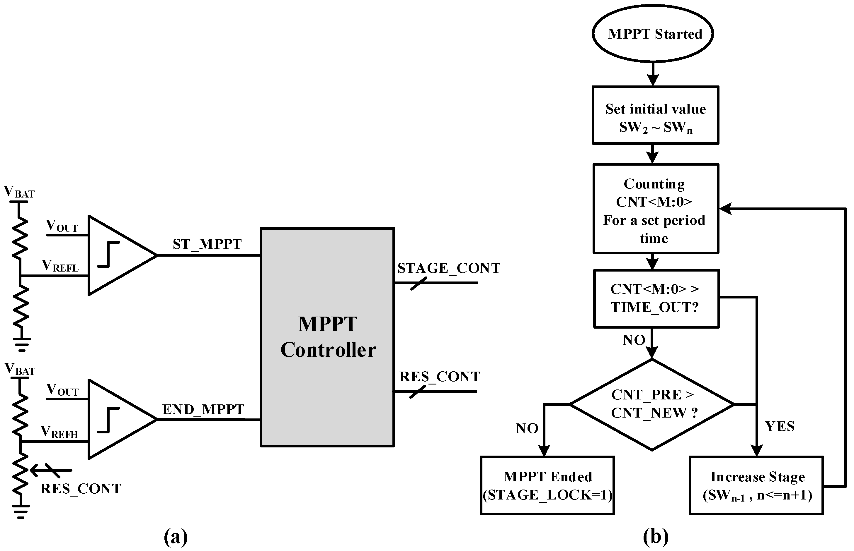
Figure 5a,b shows the block diagram and flowchart of the proposed Maximum Power Point Tracking (MPPT), respectively, to control and adjust RF–DC converter stages by adding and controlling the switches shown in
Figure 4. Since RF power isn’t a constant quantity and can vary under different environments, the load can consume the harvested energy immediately even in the low power applications. Therefore, the optimization of RF energy harvesting must be carried out under the worse possible conditions. The proposed RF–DC converter employs MPPT algorithm which automatically selects the number of stages based on the RF input power level and maintains the maximum PCE at the output. The proposed MPPT scheme consists of MPPT controller, reference generator (V
BAT) and comparators. The MPPT controller selects the stage and optimizes the control switch signals in order to determine the optimum number of stages. The control switches (
,
) are merged in each stage of the reconfigurable RF–DC converter in order to control the number of stages.
Figure 6 shows the timing diagram of the proposed MPPT to select the optimum number of stages by controlling the switches. The proposed MPPT algorithm used a digital counter to measure the charging time of V
OUT from V
REFL to V
REFH. When 1-stage is turned on, (switches
to
are turned-on while switches
to
are turned-off), the internal counter counts the charging time of the output voltage V
OUT and saves as M. Similarly when 1-stage and 2-stage are turned on, (
,
to
are turned-on while
and
are turned off), the internal counter makes L a new counted value w.r.t charging time of V
OUT. These two consecutive counted values, M and L, are then compared. If L is smaller than M, the rate of charging time increases and the output power is increased. On the other hand, if L is larger than M, the rate of charging time decreases, and the output power is decreased when 1-stage and 2-stage are turned on. This algorithm continuously decreases the counted value until the N number of stages is enabled and vice versa. The MPPT controller locks with the corresponding switches and completes the MPPT algorithm.
Figure 7 shows the operation of the nth stage of the proposed scheme during the positive phase and negative phase. During the positive input cycle, the M
n−1 and M
n transistors, in the primary rectification body, are forward-biased and are back compensated by transistor M
na in the auxiliary block. This reduces the threshold voltage of the transistors M
n−1 and M
n and increases the forward conduction current to the output. The terminal voltage V
sg of the M
nb transistor is less than the threshold voltage which makes it turned-off. During the negative input cycle, the M
n−1 and M
n transistors are reversed-biased, which sufficiently increases the terminal voltage V
sg of transistor M
nb to turn on while reducing the V
sg of M
n−1 and M
n to zero. This results in a reduced leakage current.
The source-gate voltage V
sgn of M
n transistor increases continuously with the increase of the output voltage V
OUT. The M
n transistor drives the adjacent M
n−1 transistor into the saturation region once V
sg of the M
n becomes equal to the threshold voltage. The C
Auxn capacitor stores the charge that is lost during the reverse-biased conduction.
By applying Kirchhoff’s voltage law (KVL) at the nth stage in
Figure 7, we get:
By adding (4) and (5), we get:
V
sd (n−1) and V
sdn are the voltage drop across M
n−1 and M
n transistors, respectively, and V
Auxn is the voltage drop across the C
Auxn capacitor.
By inserting the value of V
IN from (7) into (4), we get:
Subtracting (9) from (8) results in:
V
sg (n−1) and V
sgn are the gate-source voltage of the M
n−1 and M
n, respectively. Once V
sgn is equal to the threshold voltage, the M
n−1 transistor enters the saturation region. Hence, we can rewrite (6) as:
where, V
th (Mn−1) and V
th (Mn) are the threshold voltages of the M
n−1 and M
n transistors, respectively. Hence, we can minimize the threshold voltage effect over the DC-output voltage.
4. Experimental Results
The proposed low-power reconfigurable internal threshold compensated RF–DC converter is designed and implemented in 0.18 µm CMOS technology.
Figure 8 shows the layout pattern of the chip. A five-stage internal threshold compensated converter occupies an active die area of 360 µm × 160 µm, while Maximum Power Point Tracking (MPPT) occupies an active die area of 730 µm × 280 µm.
This section presents the simulated PCE of the proposed low-power reconfigurable RF–DC converter. The simulation is performed at a frequency of 900 MHz.
Figure 9a shows the simulation graph of power conversion efficiency versus RF input power for different stages having a 1 MΩ load. The RF input power level ranges from 3.16 µW to 100 µW (−25 dBm to −10 dBm). The proposed RF–DC converter exhibits different PCEs for different number of stages. It can be seen from
Figure 9a that the PCE of 1-stage RF–DC converter increases when we increase the input power from −25 dBm to −20 dBm. Also, PCE starts to decrease gradually when the input power is further increased. Similarly, the PCE of the proposed five-stages RF–DC converter increases when the input power increases from −25 dBm to −15 dBm and then starts decreasing with further increase in input power. The auxiliary block consumes the additional power, preventing the transistors in the primary rectification chain from achieving high PCE when they are forward-biased. The proposed five-stages RF–DC converter achieves a maximum simulated PCE of 39.3% at the input power of 31.6 µW (−15 dBm) for a 1 MΩ load.
Figure 9b shows the simulation results of the output DC voltage versus RF input power. The output DC voltage of each stage increases with the increase of input power. The proposed five-stages RF–DC converter delivers a 3.3 V output DC voltage for the 1 MΩ load.
Figure 9c shows the PCE of the proposed five-stage RF–DC converter for different load conditions. The proposed circuit with a 1 MΩ load has better PCE than that with a 500 KΩ load for an input power ranging from −25 dBm to −13 dBm. When the input power is further increased, the proposed circuit with the 500 KΩ load has better PCE than that with the 1 MΩ load. The proposed scheme achieves a simulated PCE of 41.7% at an input power level of 63.09 µW (−12 dBm) for a 500 KΩ load condition.
Figure 9d shows the output DC voltage of the proposed five-stage RF–DC converter for different load conditions. With the decrease in load resistance, the proposed scheme delivers less output DC voltage as compared to high load resistance. The proposed scheme produces an output DC voltage of 2.2 V at an input power level of 31.6 µW (−15 dBm) to a 500 KΩ load.
Table 1 compares the performance of the proposed scheme with recent state-of-the-art works. The proposed scheme achieves the highest performance with a PCE of 39.3% at an input power of −15 dBm and delivers a 3.3 V output DC voltage for a 1 MΩ load.

 ,
, 


