Abstract
In this paper we devise a neural-network-based model to improve the production workflow of organic solar cells (OSCs). The investigated neural model is used to reckon the relation between the OSC’s generated power and several device’s properties such as the geometrical parameters and the active layers thicknesses. Such measurements were collected during an experimental campaign conducted on 80 devices. The collected data suggest that the maximum generated power depends on the active layer thickness. The mathematical model of such a relation has been determined by using a feedforward neural network (FFNN) architecture as a universal function approximator. The performed simulations show good agreement between simulated and experimental data with an overall error of about 9%. The obtained results demonstrate that the use of a neural model can be useful to improve the OSC manufacturing processes.
1. Introduction
The basic design constraints in organic solar cells (OSCs) influence significantly the energy absorption by light trapping and the consequent conversion efficiency. OSC electrical characteristics strongly depend on the device’s geometry [1,2,3,4]. Among such geometrical values, the cell surface dimension and the thickness, particularly the active layer thickness, influences the performances of the solar cell. Such electrical performances can be devised by means of several parameters such as carrier mobility, the donor–acceptor ratio, the materials’ concentrations, and the morphology of the blend [5,6,7,8,9,10,11]. Moreover, in solar cells, electron-hole pairs are formed when light is absorbed. Unfortunately, some electrons-hole pairs can recombine before they reach the external circuit. In this latter case, the recombined pairs do not contribute to the produced electrical current; thus, these pairs reduce the conversion efficiency of the solar cell.
Also found in the literature [12] is that OSCs’ electrical output is affected by the optical properties of a device’s blend film, so it is paramount to determine the right thickness of the active layer for OSCs to achieve optimal behavior. In [13], the authors present a particle swarm optimization algorithm to devise a two-dimensional model for multilayer bulk heterojunction organic nanoscale solar cells. Such a model takes into account the active layer thickness and the device’s morphology in order to optimize electrical performances. In [14], an iterative Levenberg–Marquardt optimization algorithm was developed to investigate the dependence of the electrical characteristics from the aluminium oxide layer’s thickness in relation to several chemical parameters, such as the amount of sulphuric acid, the amount of oxalic acid, the amount of aluminium cations, the electrolyte temperature, and the anodizing time. In this paper, we propose an optimized production process, improved by means of a neural network, to reduce both cost and time. The developed neural network can be used to model the OSC and determine its efficiency based on its geometrical and optical characteristics.
The paper is structured as follows: In Section 2, we discuss the device fabrication techniques and the related production workflow, and illustrate the improvement proposed in this paper. In Section 3, we describe the adopted experimental procedure for the production of several prototypes and their analysis with AFM measurements and the determination of their electrical characteristics. In Section 4, the basis of the neural network modeling techniques are reported, while the used implementation and the obtained results are shown in Section 5. Finally, in Section 6, we draw our conclusions.
2. Device Fabrication Workflow
Many different layer processing techniques have been recently developed, and many of them are suitable for OSC production. On the other hand, the produced OSC performances have been considered dependent on a delicate and highly empirical relationship between the processing method, the solvents, the additives, the drying, the materials, the substrate, and perhaps even the operator [15,16,17,18,19,20,21]. It follows that the production workflow is strongly affected by an unavoidable, and often extensive, cycle of tries and tests until optimal manufacturing solutions are finally found. The said production workflow is generally characterizes by the following steps:
- technology selection;
- geometric design;
- prototype manufacturing;
- AFM measurement;
- electrical characterization;
- prototype testing;
- prototype evaluation;
- mass production or rejection.
Firstly when a technology is selected determining the chemical compounds to be used, a design phase should follow to define the geometrical characteristics of the prototype, aiming to find a suitable solution that can optimize the optical and electrical performances of the device. After the prototype manufacturing, a series of studies are performed on it, such as AFM measurement and electrical characterization. The latter is paramount for the prototype testing phase when the electrical performances are determined. Finally, once the data has been collected, the prototype is evaluated in order to decide whether it can be produced or not [22]. In the latter case, the prototype is rejected, and the production workflow starts again until a suitable solution is found for the mass production of a finalized device. Unfortunately, proportionally with the number or tries, the development cost of a device could grow exponentially, therefore tampering with the OSC’s production convenience and feasibility.
In this paper, we deal with the development cycle growth devising a functional model for the OSC prototype based on neural networks. Consequently, instead of an undetermined number of tries, it suffices to produce several prototypes for a chosen technology, in order to train a neural network to model the device behavior based on a set of optical and geometrical parameters. The neural network model study can be easily integrated into the production workflow as a complementary step between the AFM-electrical characterization and the production of an engineered device (see Figure 1).
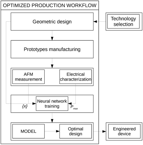
Figure 1.
The proposed improvement to the production workflow of organic solar cells (OSCs): a neural network module is introduced in order to determine a model of the OSCs’ electrical characteristics in order to devise their optimal design.
3. Experimental Prodcedure
In the following, we will show how the introduced neural network modeling technique has been integrated into the said production workflow and the related results.
3.1. Device Manufacturing
In order to investigate the thickness of layers in OSCs, we prepared and manufactured 80 samples using flexible and conductive organic materials (Figure 2). The produced samples have an active layer area of mm × mm and implements indium tin oxide (ITO)-coated glass substrates of a mm × mm surface and a mm thickness, with a resistance of 20 Ohm/m. The said substrates are rinsed and sonicated in an acetone, methanol, and isopropyl solution for 15 min each. Afterwards, the substrates are treated in a plasma oven to remove organic residues for 5 min. A water solution of poly (3,4-ethylenedioxythiophene) polystyrene sulfonate (PEDOT:PSS) is spin-coated on substrates at 5000 rpm and annealed for an hour at a temperature of 100–105 °C. This latter process is necessary to remove the water and solidify it as a layer. The next step, performed into a glove-box, requires the blending of a compound of polythiophene and phenyl-C61-butyric acid methyl ester (PCBM:P3HT) layer with a weight ratio of 1:1, and this compound is dissolved in chloroform trichloromethane (CHCl). The solution is then stirred for one hour with a magnetic stirrer and finally spin-coated on substrates for one minute at 1000 rpm. All samples are annealed at 105 °C for an hour and transferred inside the thermal evaporator, where aluminum cathodes, approximately 80 nm thick, are evaporated on the samples (Figure 3).
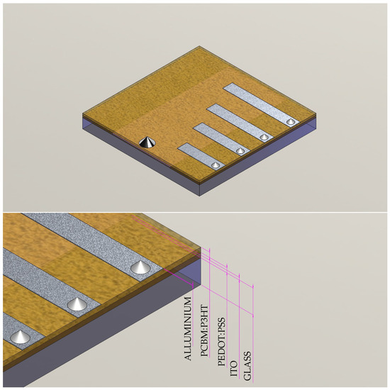
Figure 2.
A representation of the geometry of a device containing four OSCs. On the bottom panel, a detail of the layers composition of the OSCs.
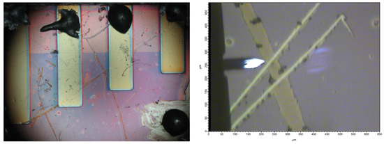
Figure 3.
On the left, an optical microscopy image of one the prototypes captured with a Zeiss Stereo Discovery.V12 microscope. On the right, a SEM image of a scratched sample.
3.2. Morphological Study
The device’s morphological studies have been performed on samples as shown in Figure 3 with Zeiss Stereo Discovery V12 microscope (Zeiss, Oberkochen, Germany) with a digital camera Zeiss 4.0×, under magnification of 150×. The topographical analyses are carried out using an atomic force microscope (AFM) (Asylum Research, Santa Barbara, CA, USA). Initially, we scratched the aluminum and located the samples under the AFM microscope. We then analyzed the surface profiles of 8 samples. Each surface profile was sampled at 512 equidistant points with a scan rate of 0.50 Hz, namely the frequency to complete a trace–retrace cycle. Each image was composed of 256 lines. The optoelectronic studies ran under simulated air mass (AM) 1.5 solar irradiation with a power density of 100 mW cm using a Stellar Net spectrometer (Stellar Net, Tampa, FL, USA), while measurements were analyzed using a Keithley Model 2420 SourceMeter instrument (Tektronix, Bracknell, UK). The measurement of generated power, in terms of current–voltage characteristics (I-V curve), was measured at room temperature under AM 1.5G conditions using a solar simulator (Steuernagel Lichttechnik, Morfelden-Walldorf, Germany) with a wavelength range of 300–750 nm.
3.3. AFM Measurements
The AFM can provide accurate 3D surface profiles at atomic resolution, measuring the force at a nano-newton scale by a laser beam deflection system. Measuring the topography can reveal information on the film structure including roughness, texture, abrasion, adhesion, cleaning, corrosion, etching, friction, lubrication, plating, and polishing. The AFM forms the image without lenses, using a very thin tip trace at the end of a flexible lever (cantilever), performing a scan on the surface of the sample. AFM tips and cantilevers are typically fabricated from Si or SiN. A typical tip radius is from a few to 10 s of nm. During the scanning, the interaction and magnetic surface forces are established between tip and sample and are typically less than N, which determine cantilever bending and the subsequent detection of the surface topography (Figure 4). The cantilever deflections can be detected up to 0.01 nm via an optical detection system consisting of a laser and a photodiode. The laser beam is reflected by the back of the cantilever towards the photomultiplier and then converts the solar energy to voltage, amplifying the incoming signal. The photodiode measures the difference in light intensities between the upper and lower photodetectors, proportional to the cantilever deflection. In conditions of null deflection, the difference signal is assumed equal to zero. Through this system, the cantilever movements are amplified several times. The sample is placed on a miniature piezoelectric tube designed to move along the system of crystallographic axes . Piezoelectric tube is made of a particular material (piezoelectric ceramics) that is able to expand or change the response subjected to an electric field. An AFM image is typically comprised of a signal representing some Z distance of cantilever motion per X,Y point on the scan raster. All signals are typically read as a voltage in the software control system. For biology applications and material science, different modes of operations are used for the system such as intermittent contact mode (called AC mode). In contact mode, the tip is in full contact with the surface as the sample is rastered in an XY pattern, and maintains a user-defined deflection voltage (i.e., the force on the tip is repulsive, with a mean value of N to keep a positive deflection on the cantilever).
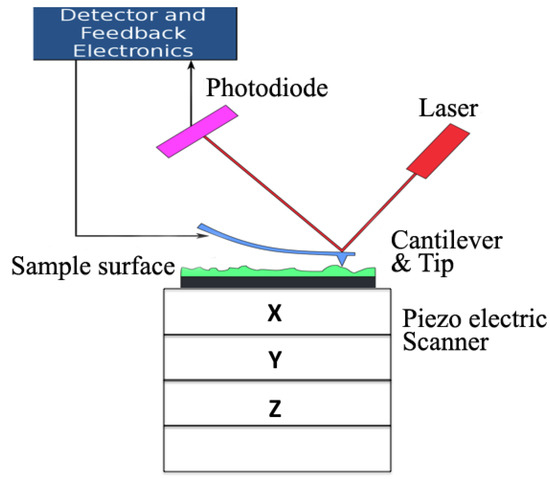
Figure 4.
A schematics of the AFM piezoelectric scanner: the tip scans the surface and the resulting cantilever deflections are detected from an optical system consisting of a laser, a set of lenses, and a photodiode.
3.4. Data Acquisition
AFM can reveal a sample surface and precisely up to nanometer size in three dimensions. We have analyzed the surface profiles of 80 samples produced at the Optoelectronic Organic Semiconductor Devices Laboratory at Ben Gurion University of the Negev (Figure 5). Each surface profile was sampled at 512 equidistant points with a scan rate of 0.50 Hz, namely the frequency to complete a trace–retrace cycle. Each image was composed of 256 lines. The scan size varied between 30 and 60 μm. A thermal tune was performed to determine the natural resonant frequency of the cantilever by monitoring the amplitude over a user-defined frequency range. During the measurements, the AFM tip was excited at the resonant frequency to obtain a free oscillating amplitude that corresponds to 800 mV output of the integrated detector (Set Point) with an intergral gain of 12.76. The resonance curve of the cantilever obtained in AC mode is expected to peak around 200–400 kHz. The (Version 13, Revision A-1715, Asylum Research, Santa Barbara, CA, USA) allows one to better ensure that the tip experiences net repulsive forces with the sample as it interacts with the surface. Based on the height profile, pixel histograms from images can be counted and plotted. The Histogram Graph appears with a pixel count (Y) relative to the Z scale (X). The histogram method is used to determine the thickness. The whole range of height difference is divided into small pieces, each of which is counted by statistics. By fitting these histogram peaks using Gaussian equations, the height difference (175 nm for P3HT:PCBM and 4 nm for PCBM:PEDOT) and the ITO substrate can be accurately determined. We evaluated the current as a function of different film thicknesses for active layers. The current increases typical for film thicknesses over 50 nm and near 250 nm are shown in Figure 6. The problem in OSCs, especially in -conjugated polymers, is mainly related to the low charge carrier mobility exhibiting reduced Langevin bimolecular charge recombination. The recombination of free charge carriers (electron and holes) is often described with the Langevin recombination rate expressed by
where e is the electron charge, the Langevin-type bimolecular recombination coefficient, the mobility of electrons and holes, and the relative dielectric permittivity. The recombination could be influenced by the active layer thickness, nevertheless physical parameters, electronic properties, and defects contribute mostly.
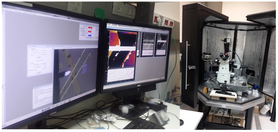
Figure 5.
The laboratory in the Ilse Katz Institute for Nanoscale Science and Technology at Ben-Gurion University of the Negev, where the devices have been analyzed.
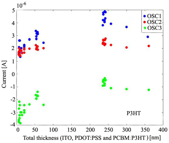
Figure 6.
Current as a function of active layer thickness (ITO, PEDOT:PSS, PCBM:P3HT) for three different OSC samples (labeled OSC1, OSC2, and OSC3).
The experimental data collected during our measurement campaign suggested that the maximum generated power depends on the active layer thickness (see Figure 7). It was observed that optimal efficiency, in terms of generated power, can be obtained by using specific thickness configurations (e.g., by using a PEDOT:PSS films 40 nm thick and a PCBM:P3HT of 180 nm, see Figure 8).
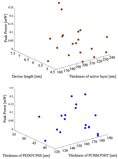
Figure 7.
The figure shows the results of the trained neural network. On the top, the dependence of the generated power from the total thickness and length is reported. On the bottom, the power as a function of the PEDOT:PSS and PCBM:PSS thicknesses is shown.
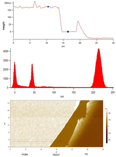
Figure 8.
Extraction profiles of PCBM, PEDOT, and ITO. Top to bottom: the profile collected by Z sensor channel; a histogram of the height difference between PCBM:PEDOT and ITO; 2D topographical image.
These experimental results suggests that it exists a highly non-linear relation between power and active layer thickness. Our purpose here is to devise such a non-linear relation. In order to model such a relation, we used a neural-network-based architecture due to its well known ability to approximate mathematical functions, as will be described in the following.
Since the entire physical structure of an OPV affects the obtained performances, we used the neural network to reckon the relation between the generated power (network output) and the following input parameters.
- PEDOT:PSS thickness ();
- PCBM:P3HT thickness ();
- overall device thickness (t);
- overall device length (l);
- overall device height (h).
The basics of the adopted neural modeling technique will be described in the following.
4. Neural-Network-Based Modeling
A typical application of neural networks is to extract and identify useful relationships/structures in complex systems, frequently for several available data and mostly containing a little information. The neural network is composed by nodes, input, hidden, and output units connected by links with associated numeric weights . The output of each unit is expressed as a function of its input , and an activation function g is then applied to the weighted sum of inputs. To parametrize the behavior of the activation functions, the bias weight is used:
By adjusting the weights at each step and by changing the function of the network, the learning procedure is defined. The feed-forward neural network (FFNN) has three layers of neurons: an input layer, one or more hidden layers, and an output layer with neurons connected with the layers and input units. In a similar fashion, a neural network can be represented as a directed graph composed by a finite number of nodes, called neurons, and weighted edges, called connections. The neurons are organized in layers: an input layer, an output layer, and a variable number of hidden layers. The neurons of each hidden layer are called hidden neurons. This latter uses the output of the previous layer’s neurons as an input weighted by means of the related connections’ weights, and computes on such input a function (called activation totransfer function). In a general formulation, suppose an N-dimensional input such that
We will define input layer the set of neurons so that
Given the l-th hidden layer, it can be similarly formalized as
where is the output of the j-th neuron of the l-th layer (composed by neurons), its activation function, and the bias; is the number of neurons in the previous layer; is the connection weight from the i-th neuron (with output ) on the -th layer (composed by neurons) to the j-th neuron on the L-th layer. The output layer will be composed of M neurons with a value given by
Neural Networks as Universal Approximators
As is well known [23,24,25], any Riemann-integrable function, that we will call signals, can be arbitrarily approximated by means of an FFNN regardless of the activation function or input space, while signals with a finite support can be exactly approximated by a single layer of neural units. Although similar to the Cybenko–Hornik theorem, it must be highlighted that the MLP approximation theorem does not need a continuous signal among its hypothesis. An FFNN [26] can approximate signals using two hidden layers [27,28]: the first hidden layer approximates the signal by means of a step function such that
is the output of the first hidden layer (composed by neurons ), with respect to the input (composed by elements ), where are neural weights and is the bias used as threshold for the step function. The second hidden layer computes the height of the stair step, in which the input value lies in order to return a value to the output layer. The threshold logic units’ computation can be interpreted geometrically as they split the input hyperplane in two half-hyperplanes. In this representation, the separation line’s equation depends on the weights and bias. Such variables are determined by a training algorithm based on the overall approximation error that affects the network. On the other hand, the approximation accuracy after training strictly depends on the number of neurons, which influences the size of the stair steps.
5. The Implemented Neural Model and Results
The FFNN proposed in this paper is developed in order to obtain an approximate mathematical expression of OSC’s maximum power depending on the device’s geometrical parameters and the active layer’s thickness (PEDOT:PSS and PCBM:P3HT). The proposed neural network, shown in Figure 9, is composed of four layers: an input layer, two hidden layers, and an output layer. The input layer has five inputs (the device’s overall length, l, the height, h, the thickness, t, the PEDOT:PSS layer thickness, , and the PCBM:P3HT layer thickness, ). The two hidden layers of the implemented FFNN use logsigmoid activation functions and are respectively composed of 7 and 4 neurons. The proposed neural network has been trained to minimize its root mean squared error (RMSE) by means of a Gradient Descend with Momentum Algorithm (GDMA) [29], using the geometrical parameters and the measured thicknesses as inputs and the measured maximum power as target (see Figure 6, where three examples of the measured generated currents are reported in relation to the active layer thicknesses).
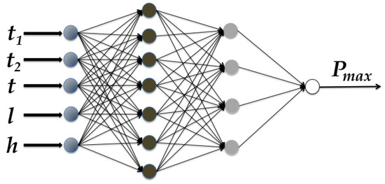
Figure 9.
The implemented feed-forward neural network (FFNN) architecture.
Figure 7 shows some of the results obtained using the neural network: respectively, the dependence of the maximum generated power from the total thickness and length of the device versus the maximum power as a function of the PEDOT:PSS and PCBM:P3HT thicknesses.
6. Conclusions
The implemented FFNN was trained by means of the experimental measurements collected on 80 devices with active layers (PEDOT:PSS and PCBM:P3HT) with different thicknesses at the Optoelectronic Organic Semiconductor Devices Laboratory at Ben Gurion University of the Negev. Once trained, the network was shown to be capable of determining the maximum power as a function mainly dependent on the active layers’ thickness, The extensive simulations show good agreement between simulated and experimental data with an overall error of about 9%. Furthermore, the simulations show that the active layer has a great influence on the OSCs’ efficiency. The neural network at hand has thus been validated as an empirical mathematical model of the relation between the thickness and the maximum power generated by OSCs. Finally, ultrathin OSCs with GLASS/ITO/PEDOT:PSS/PF3HT:PCBM/Al structures with different active layer thicknesses dependent on carrier mobility were investigated. An AFM in AC mode was used to better measure the active layer’s thickness and therefore to determinethe OSC’s maximum power by means of a dedicated FFNN. The experiments showed the effect of the thicknesses of the P3HT:PCBM and PEDOT:PSS active layers on the power conversion efficiency of the organic cell. The implemented neural architecture can be integrated in the manufacturing workflow in order to improve OSCs’ efficiency and reduce the related production costs.
Author Contributions
All the authors contributed equally to this work.
Acknowledgments
The authors would like to acknowledge the contribution to this research from the Rector of Silesian University of Technology under grant RGH 2017 No. 09/010/RGH17/0026 for Prospective Professors, which covered the costs of open-access publication. This work has been also supported by the BGU-ENEA joint lab and the ILSE-Joint Italian-Israeli Laboratory on Solar and Alternative Energies. Finally, we thank Jurgen Jopp of Ilse Katz Institute for Nanoscale Science and Technology.
Conflicts of Interest
The authors declare no conflict of interest.
References
- Lo Sciuto, G.; Capizzi, G.; Coco, S.; Shikler, R. Geometric Shape Optimization of Organic Solar Cells for Efficiency Enhancement by Neural Networks. In Advances on Mechanics, Design Engineering and Manufacturing, Proceedings of the International Joint Conference on Mechanics, Design Engineering & Advanced Manufacturing (JCM 2016), Catania, Italy, 14–16 September, 2016; Eynard, B., Nigrelli, V., Oliveri, S.M., Peris-Fajarnes, G., Rizzuti, S., Eds.; Springer International Publishing: Cham, Switzerland, 2017; pp. 789–796. [Google Scholar]
- Capizzi, G.; Lo Sciuto, G.; Napoli, C.; Tramontana, E. A Multithread Nested Neural Network Architecture to Model Surface Plasmon Polaritons Propagation. Micromachines 2016, 7, 110. [Google Scholar] [CrossRef]
- Bonanno, F.; Capizzi, G.; Lo Sciuto, G.; Napoli, C.; Pappalardo, G.; Tramontana, E. A Cascade Neural Network Architecture Investigating Surface Plasmon Polaritons Propagation for Thin Metals in OpenMP. In Artificial Intelligence and Soft Computing; Rutkowski, L., Korytkowski, M., Scherer, R., Tadeusiewicz, R., Zadeh, L.A., Zurada, J.M., Eds.; Springer International Publishing: Cham, Switzerland, 2014; pp. 22–33. [Google Scholar]
- Barnea, S.N.; Lo Sciuto, G.; Hai, N.; Shikler, R.; Capizzi, G.; Woźniak, M.; Połap, D. Photo-Electro Characterization and Modeling of Organic Light-Emitting Diodes by Using a Radial Basis Neural Network. In Artificial Intelligence and Soft Computing; Rutkowski, L., Korytkowski, M., Scherer, R., Tadeusiewicz, R., Zadeh, L.A., Zurada, J.M., Eds.; Springer International Publishing: Cham, Switzerland, 2017; pp. 378–389. [Google Scholar]
- Ye, L.; Hu, H.; Ghasemi, M.; Wang, T.; Collins, B.A.; Kim, J.H.; Jiang, K.; Carpenter, J.H.; Li, H.; Li, Z.; et al. Quantitative relations between interaction parameter, miscibility and function in organic solar cells. Nat. Mater. 2018, 17, 253–260. [Google Scholar] [CrossRef] [PubMed]
- Ye, L.; Zhao, W.; Li, S.; Mukherjee, S.; Carpenter, J.H.; Awartani, O.; Jiao, X.; Hou, J.; Ade, H. High-Efficiency Nonfullerene Organic Solar Cells: Critical Factors that Affect Complex Multi-Length Scale Morphology and Device Performance. Adv. Energy Mater. 2017, 7, 1602000. [Google Scholar] [CrossRef]
- Chen, G.; Ning, Z.; Agren, H. Nanostructured Solar Cells. Nanomaterials 2016, 6, 145. [Google Scholar] [CrossRef] [PubMed]
- Cataldo, S.; Pignataro, B. Polymeric Thin Films for Organic Electronics: Properties and Adaptive Structures. Materials 2013, 6, 1159–1190. [Google Scholar] [CrossRef] [PubMed]
- Hakim, F.; Alam, M.K. Improvement of photo-current density of P3HT:PCBM bulk heterojunction organic solar cell using periodic nanostructures. In Proceedings of the 2017 International Conference on Electrical, Computer and Communication Engineering (ECCE), Cox’s Bazar, Bangladesh, 16–18 February 2017; pp. 170–174. [Google Scholar]
- Hakim, F.; Alam, M.K. Optimization and performance analysis of PCBM acceptor-based bulk heterojunction organic solar cells using different donor materials. In Proceedings of the 2016 9th International Conference on Electrical and Computer Engineering (ICECE), Dhaka, Bangladesh, 20–22 December 2016; pp. 127–130. [Google Scholar]
- Chen, H.; Miao, J.; Yan, J.; He, Z.; Wu, H. Improving Organic Solar Cells Efficiency Through a Two-Step Method Consisting of Solvent Vapor Annealing and Thermal Annealing. IEEE J. Sel. Top. Quantum Electron. 2016, 22, 66–72. [Google Scholar] [CrossRef]
- Duan, C.; Huang, F.; Cao, Y. Solution processed thick film organic solar cells. Polym. Chem. 2015, 6, 8081–8098. [Google Scholar] [CrossRef]
- Rahmani, R.; Karimi, H.; Ranjbari, L.; Emadi, M.; Seyedmahmoudian, M.; Shafiabady, A.; Ismail, R. Structure and thickness optimization of active layer in nanoscale organic solar cells. Plasmonics 2015, 10, 495–502. [Google Scholar] [CrossRef]
- Michal, P.; Vagaská, A.; Gombár, M.; Kmec, J.; Spišák, E.; Kučerka, D. Usage of Neural Network to Predict Aluminium Oxide Layer Thickness. Sci. World J. 2015, 2015, 253568. [Google Scholar] [CrossRef] [PubMed]
- Rafique, S.; Abdullah, S.M.; Sulaiman, K.; Iwamoto, M. Fundamentals of bulk heterojunction organic solar cells: An overview of stability/degradation issues and strategies for improvement. Renew. Sustain. Energy Rev. 2018, 84, 43–53. [Google Scholar] [CrossRef]
- Schiefer, S.; Zimmermann, B.; Würfel, U. Layout optimization of organic wrap through solar cells by combined electrical and optical modeling. Solar Energy Mater. Solar Cells 2013, 115, 29–35. [Google Scholar] [CrossRef]
- Nam, Y.M.; Huh, J.; Jo, W.H. Optimization of thickness and morphology of active layer for high performance of bulk-heterojunction organic solar cells. Solar Energy Mate. Solar Cells 2010, 94, 1118–1124. [Google Scholar] [CrossRef]
- Bello, L.L.; Mirabella, O.; Torrisi, N. Modelling and Evaluating traceability systems in food manufacturing chains. In Proceedings of the 13th IEEE International Workshops on Enabling Technologies: Infrastructure for Collaborative Enterprises, Modena, Italy, 14–16 June 2004; pp. 173–179. [Google Scholar]
- Liao, K.S.; Yambem, S.D.; Haldar, A.; Alley, N.J.; Curran, S.A. Designs and Architectures for the Next Generation of Organic Solar Cells. Energies 2010, 3, 1212–1250. [Google Scholar] [CrossRef]
- Kaya, M.; Hajimirza, S. Extremely Efficient Design of Organic Thin Film Solar Cells via Learning-Based Optimization. Energies 2017, 10, 1981. [Google Scholar] [CrossRef]
- Wang, J.; Tapio, K.; Habert, A.; Sorgues, S.; Colbeau-Justin, C.; Ratier, B.; Scarisoreanu, M.; Toppari, J.; Herlin-Boime, N.; Bouclé, J. Influence of Nitrogen Doping on Device Operation for TiO2-Based Solid-State Dye-Sensitized Solar Cells: Photo-Physics from Materials to Devices. Nanomaterials 2016, 6, 35. [Google Scholar] [CrossRef] [PubMed]
- Lo Sciuto, G.; Capizzi, G.; Gotleyb, D.; Linde, S.; Shikler, R.; Woźniak, M.; Połap, D. Combining SVD and Co-occurrence Matrix Information to Recognize Organic Solar Cells Defects with an Elliptical Basis Function Network Classifier. Artificial Intelligence and Soft Computing; Rutkowski, L., Korytkowski, M., Scherer, R., Tadeusiewicz, R., Zadeh, L.A., Zurada, J.M., Eds.; Springer International Publishing: Cham, Switzerland, 2017; pp. 518–532. [Google Scholar]
- Cybenko, G. Approximation by superpositions of a sigmoidal function. Math. Control Signals Syst. 1989, 2, 303–314. [Google Scholar] [CrossRef]
- Hornik, K.; Stinchcombe, M.; White, H. Multilayer feedforward networks are universal approximators. Neural Networks 1989, 2, 359–366. [Google Scholar] [CrossRef]
- Barron, A.R. Universal approximation bounds for superpositions of a sigmoidal function. IEEE Trans. Inf. Theory 1993, 39, 930–945. [Google Scholar] [CrossRef]
- Haykin, S.S. Neural Nnetworks: A Comprehensive Foundation, 2nd ed.; Prentice-Hall: Englewood Cliffs, NJ, USA, 1998. [Google Scholar]
- Kruse, R.; Borgelt, C.; Braune, C.; Mostaghim, S.; Steinbrecher, M. Computational Intelligence: A Methodological Introduction; Springer: Cham, Switzerland, 2016. [Google Scholar]
- Zurada, J.M.; Malinowski, A.; Cloete, I. Sensitivity analysis for minimization of input data dimension for feedforward neural network. In Proceedings of the 1994 IEEE International Symposium on Circuits and Systems, London, UK, 30 May–2 June 1994; Volume 6, pp. 447–450. [Google Scholar]
- Han, S.; Pool, J.; Tran, J.; Dally, W. Learning both weights and connections for efficient neural network. arXiv, 2015; arXiv:1506.02626. [Google Scholar]
© 2018 by the authors. Licensee MDPI, Basel, Switzerland. This article is an open access article distributed under the terms and conditions of the Creative Commons Attribution (CC BY) license (http://creativecommons.org/licenses/by/4.0/).