An Enhanced Control Scheme Based on New Adaptive Filters for Cascaded NPC/H-Bridge System


Abstract
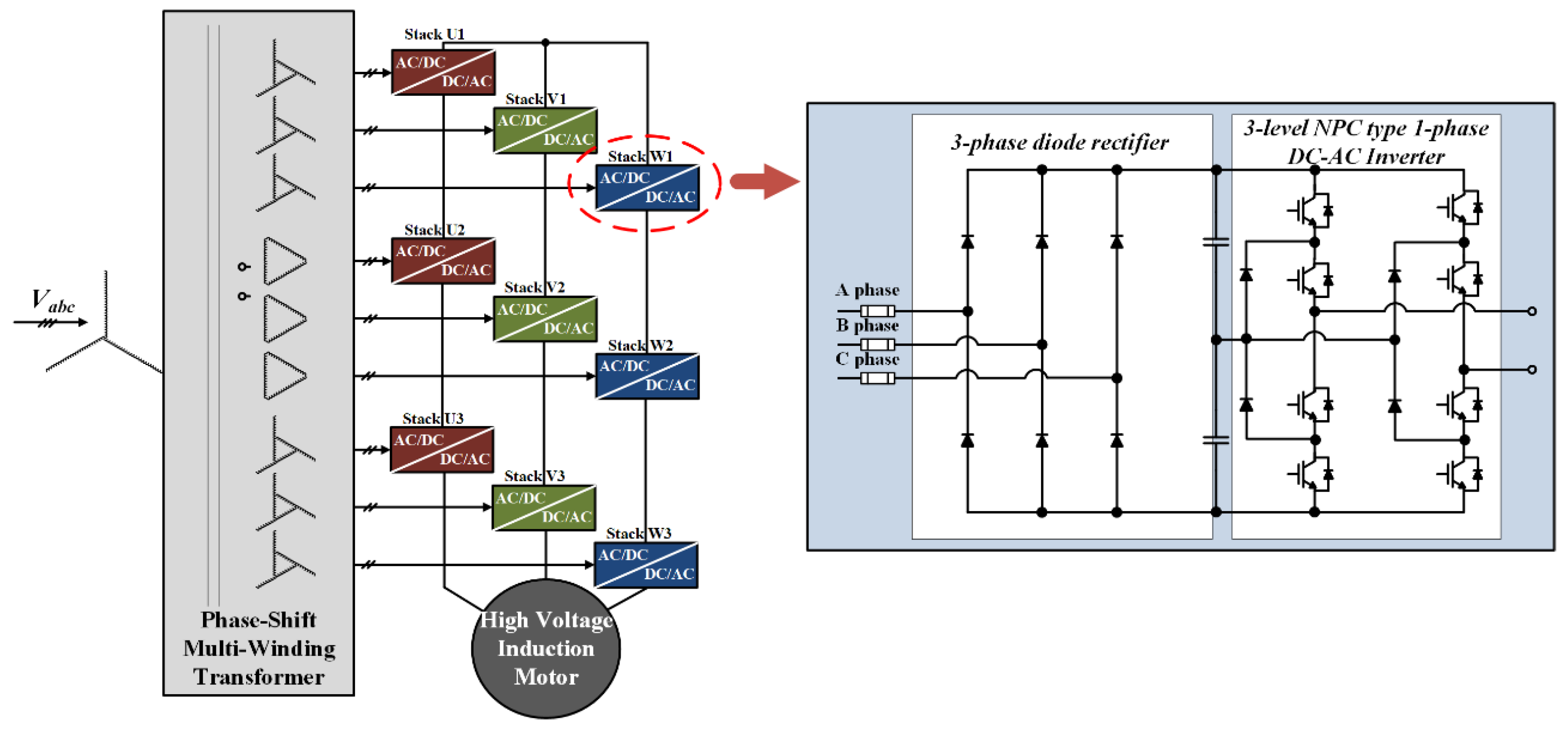
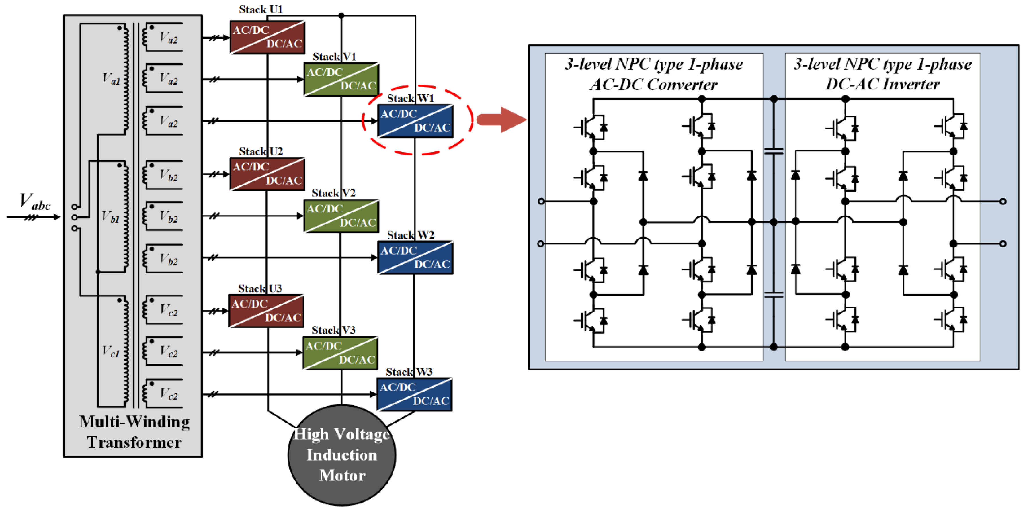
1. Introduction
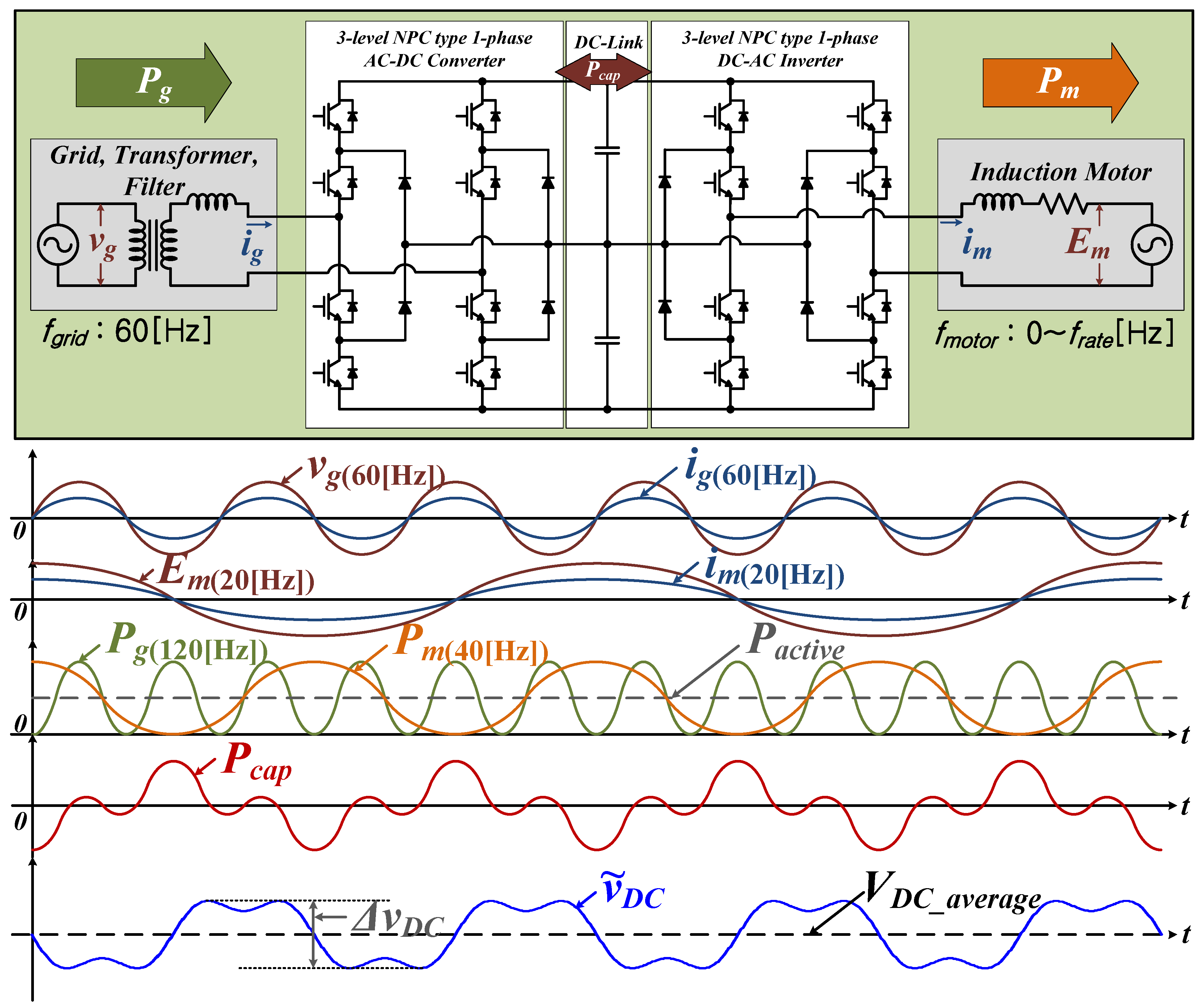
2. Analysis of the DC-Link in the CNHB System
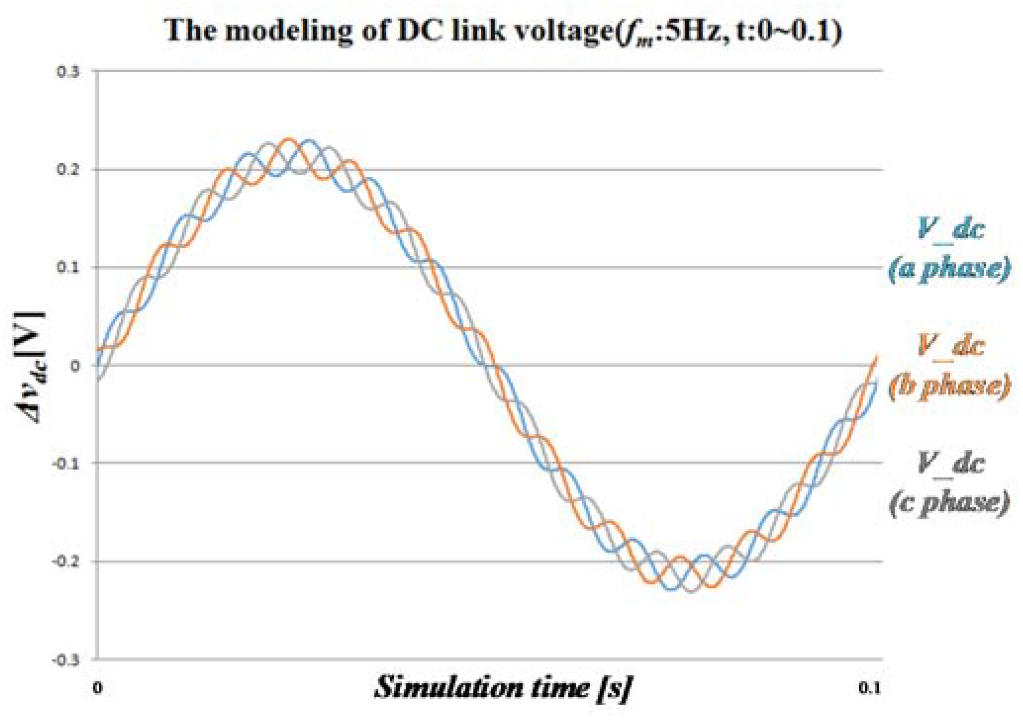
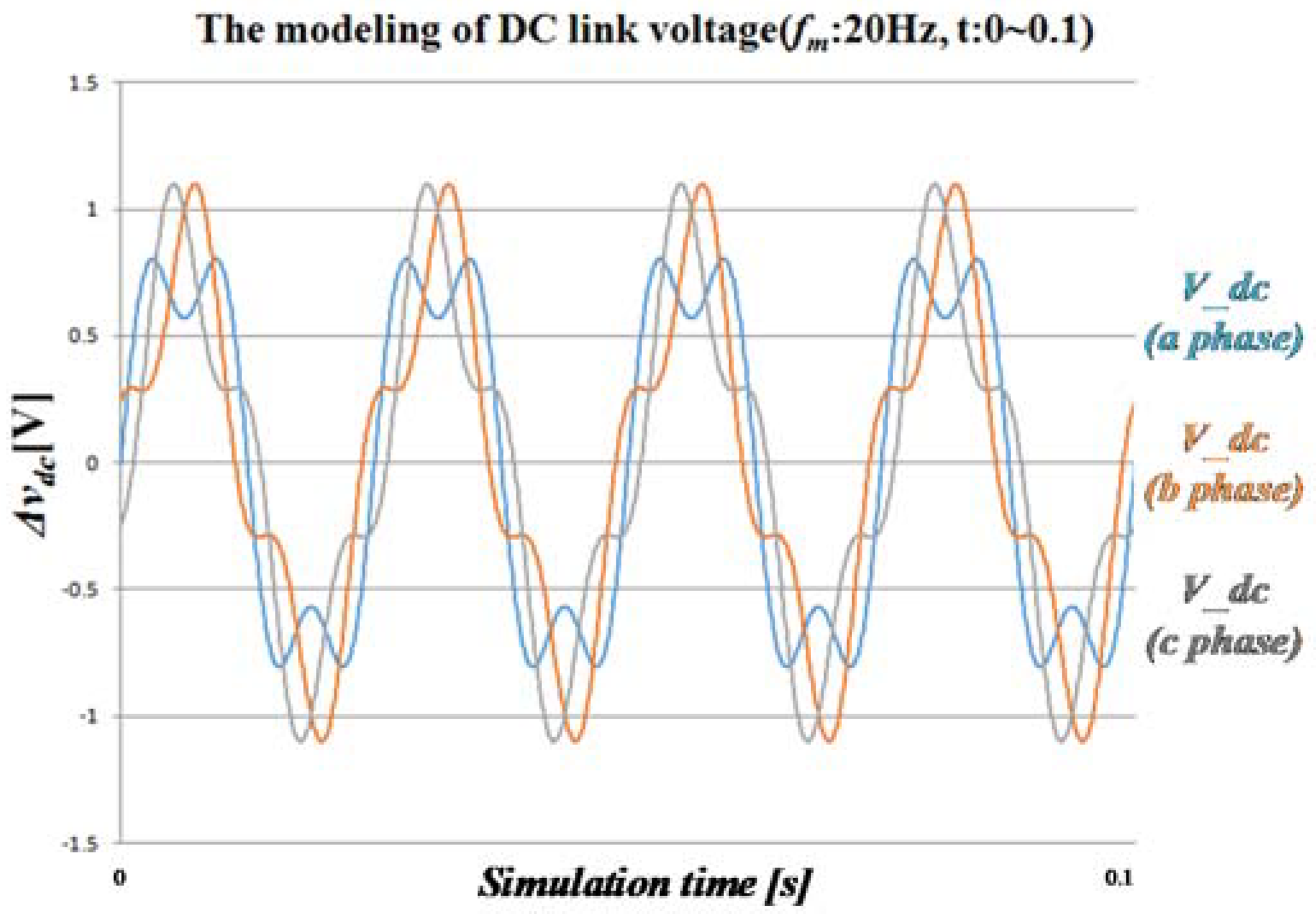
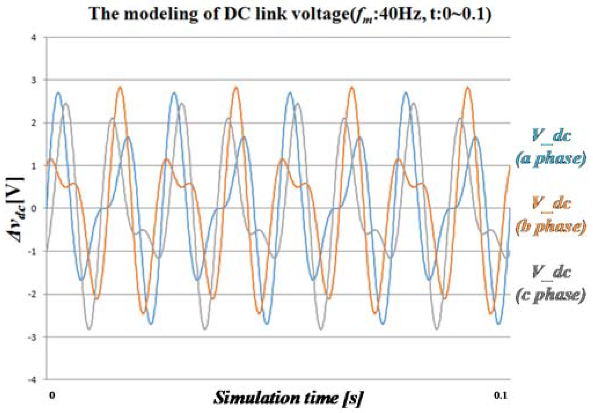
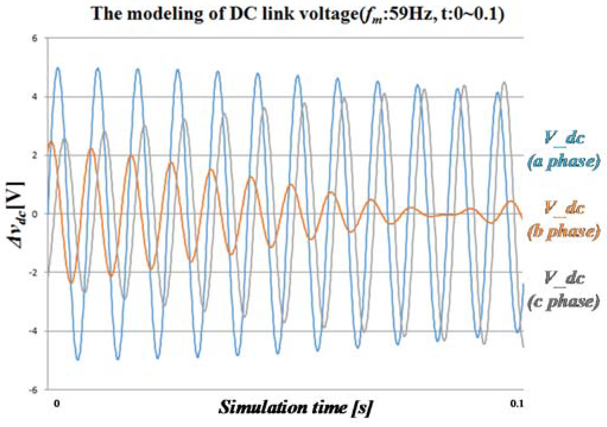
2.1. Voltage Fluctuation Analysis in the DC-Link of One Cell
2.2. Optimal Designing DC-Link Capacitor
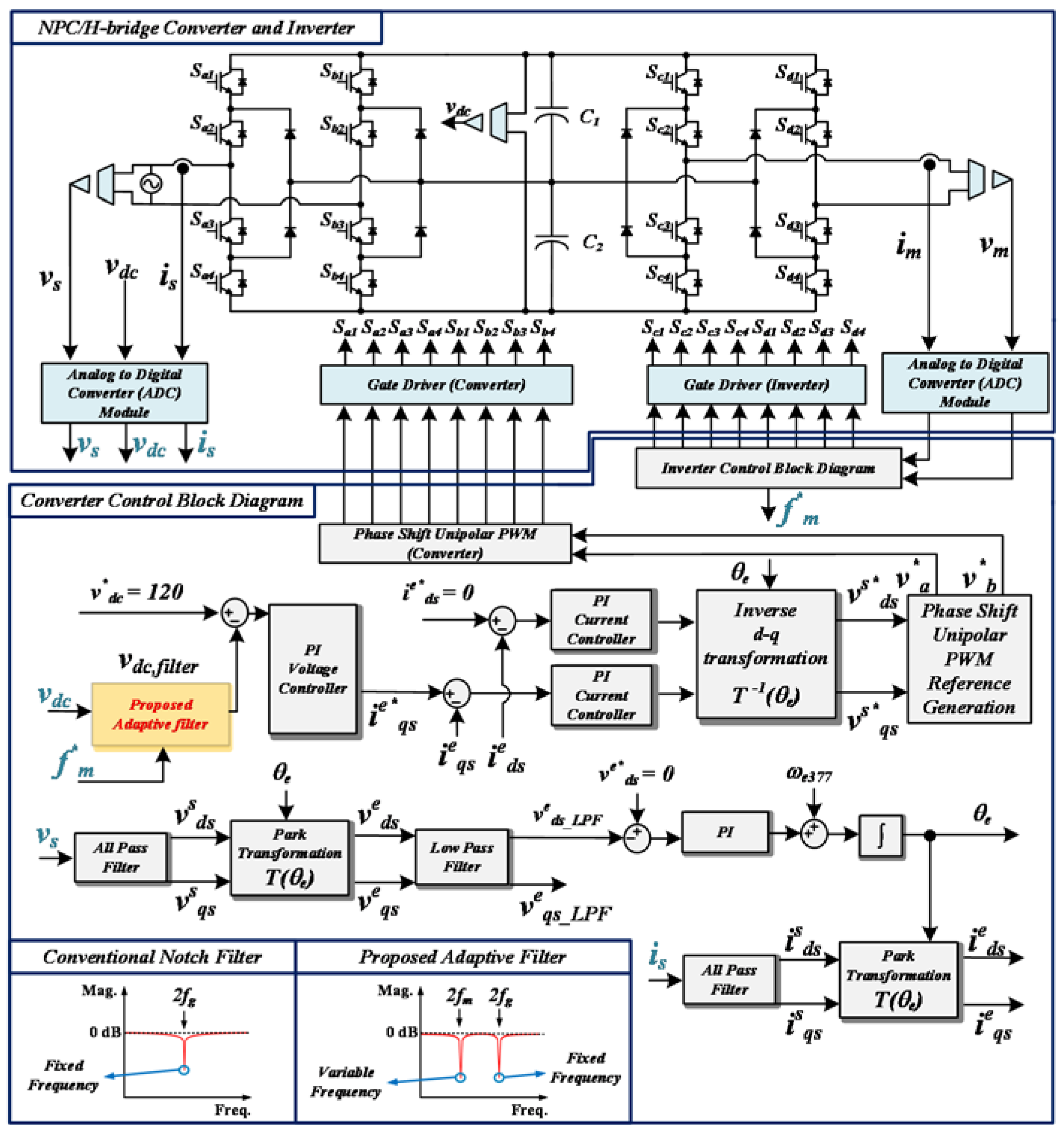
3. Proposed Control Method Using Adaptive Filters
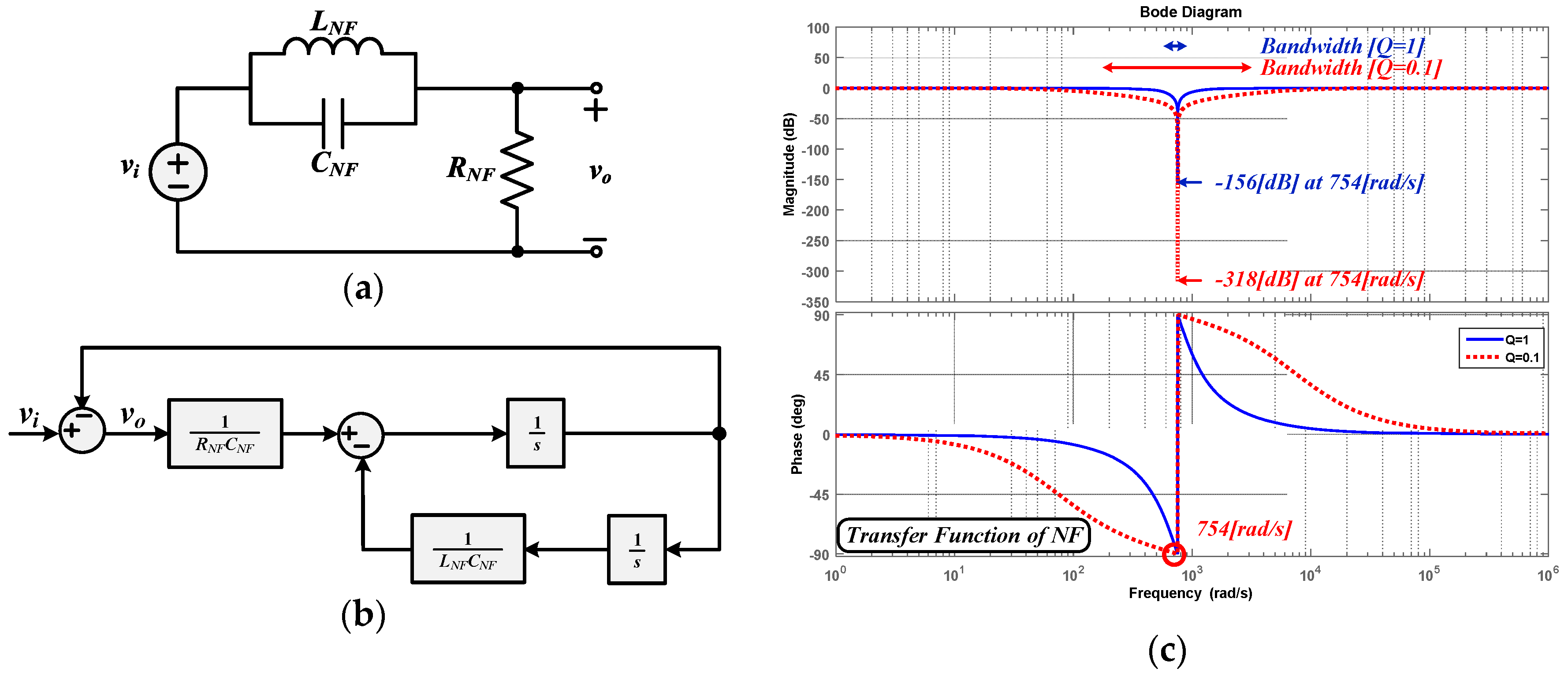
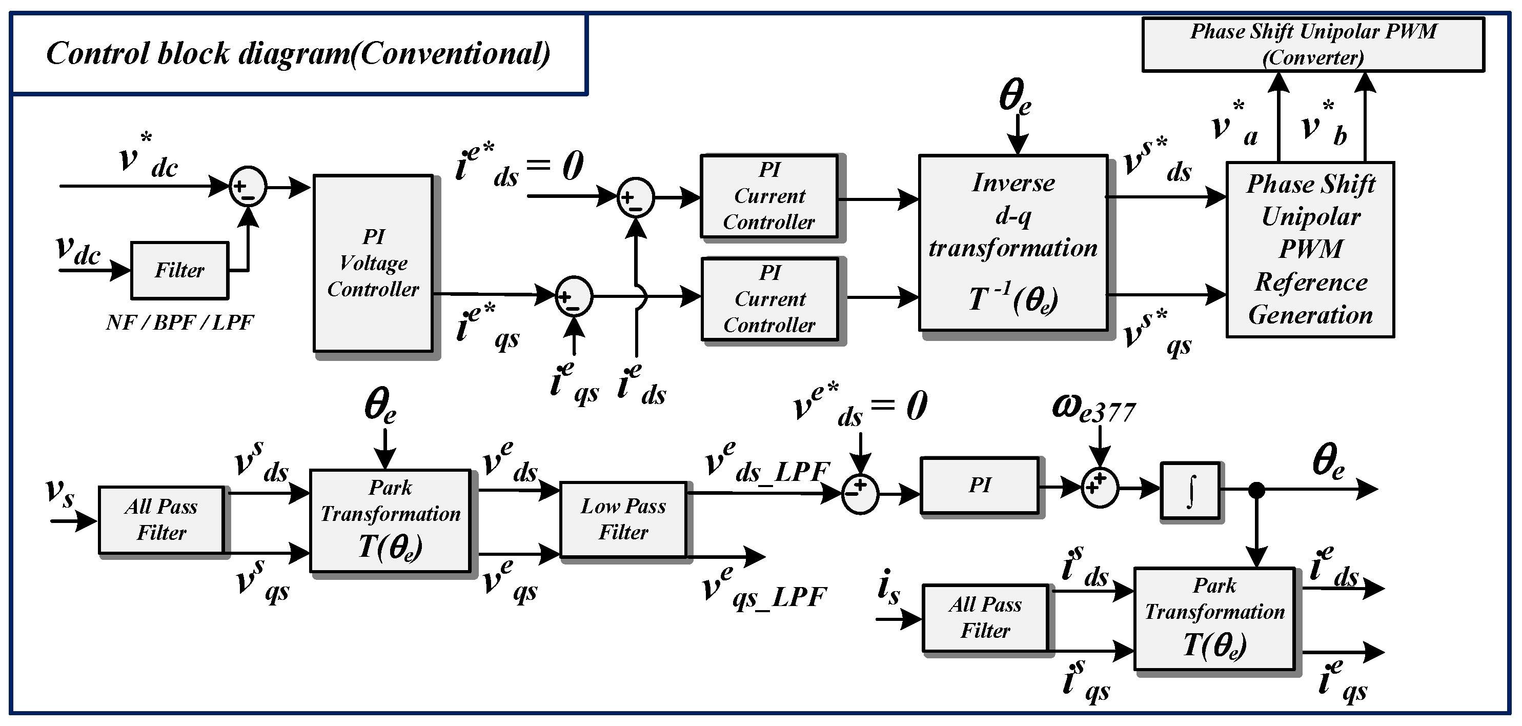
3.1. Conventional Filter
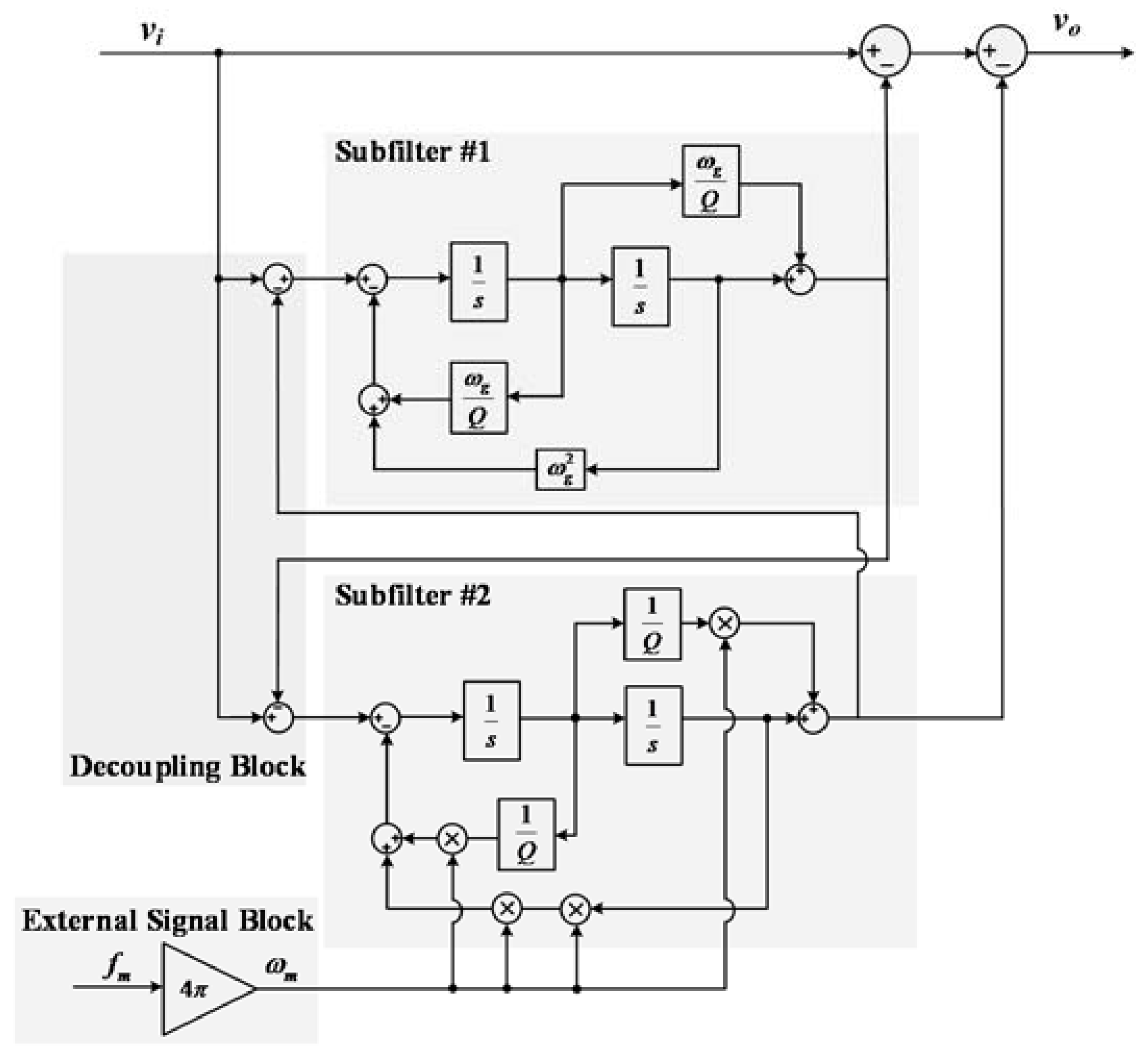
3.2. Proposed Adaptive Filters and Control Method
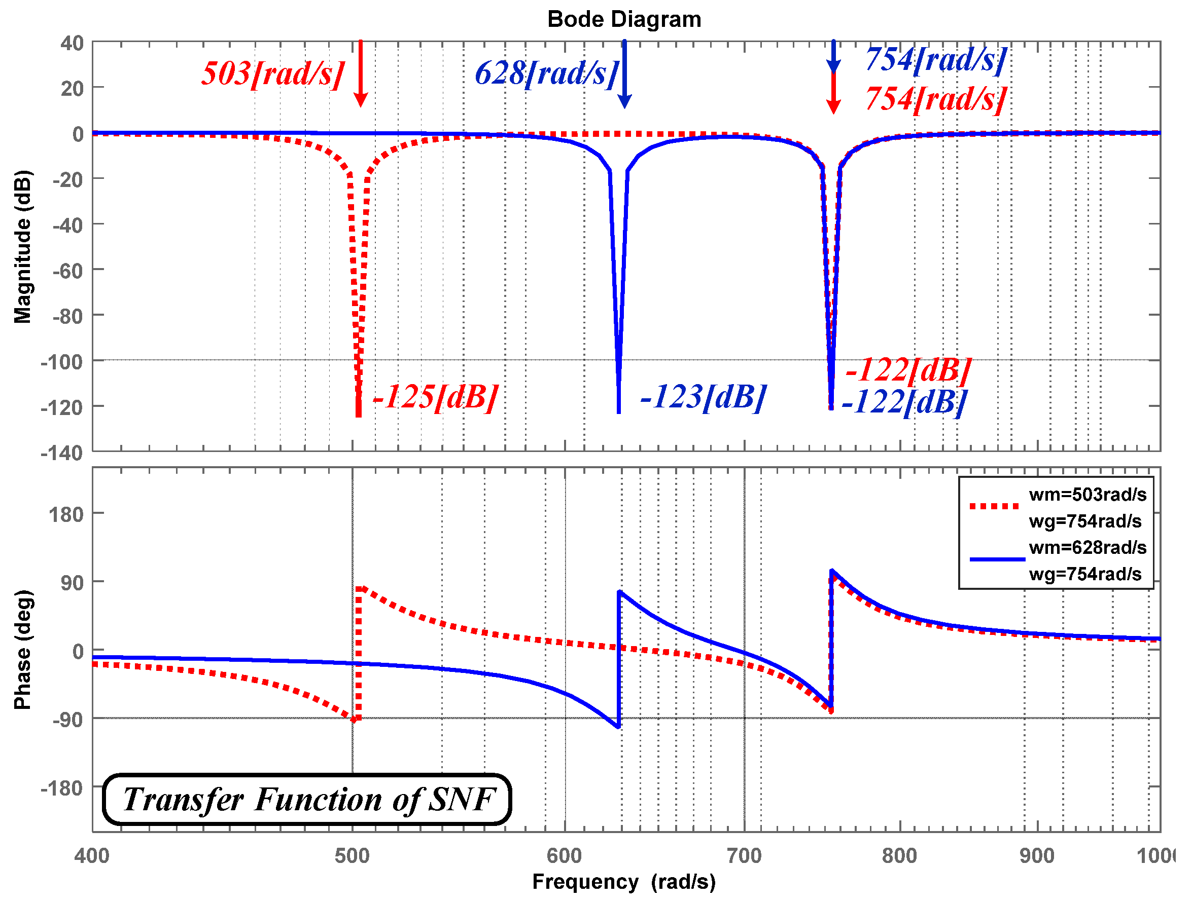
3.2.1. Series Notch Filter
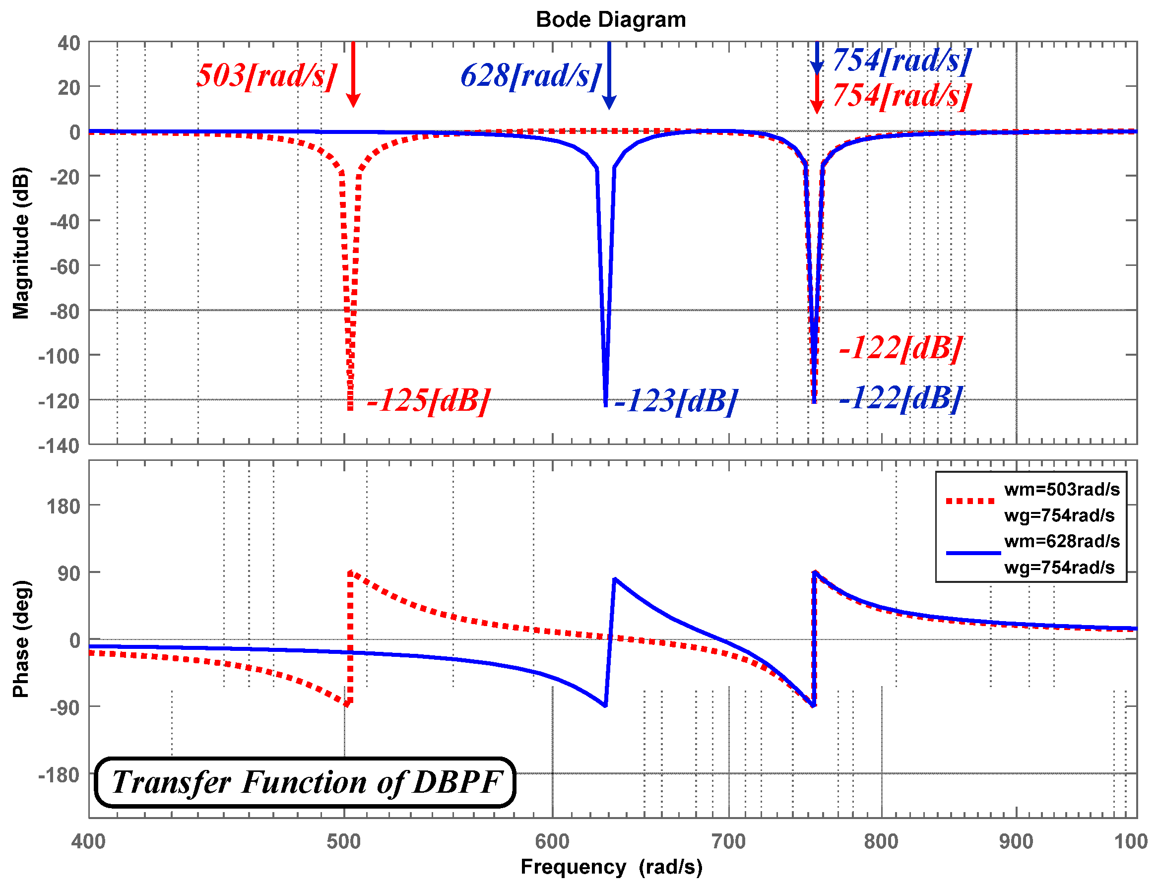
3.2.2. Decoupled Band Pass Filter
3.2.3. Control Method
4. Simulation Results
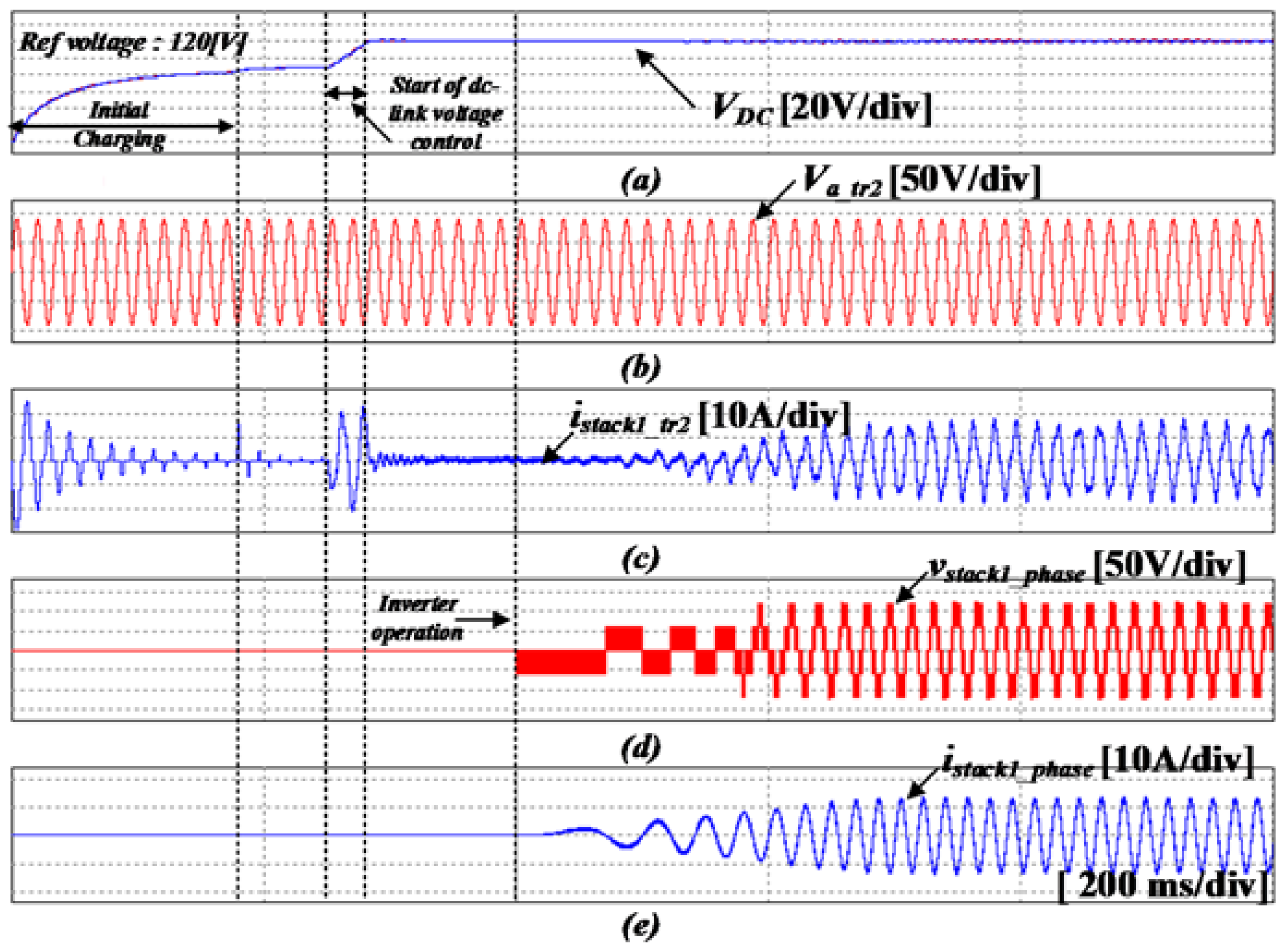
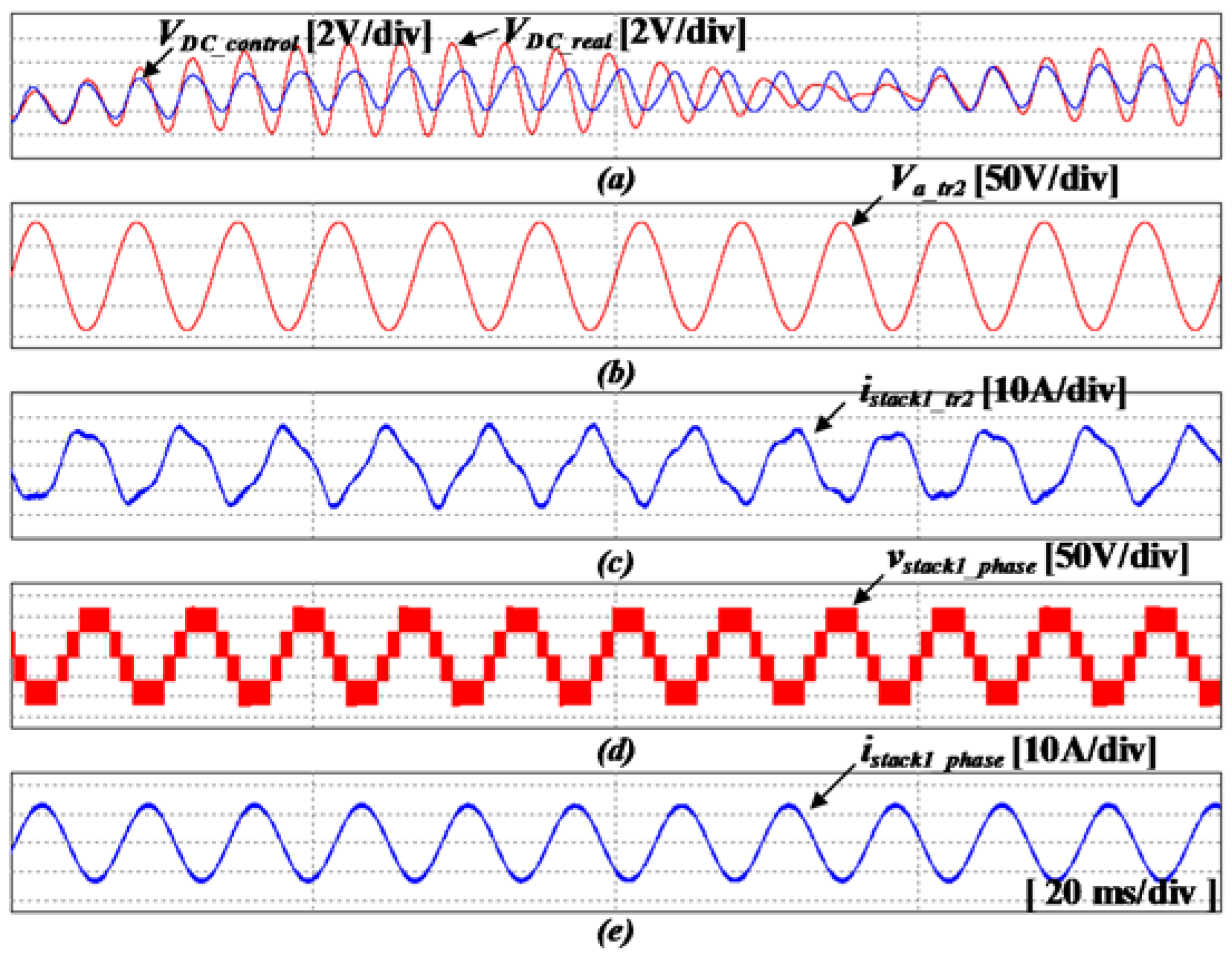
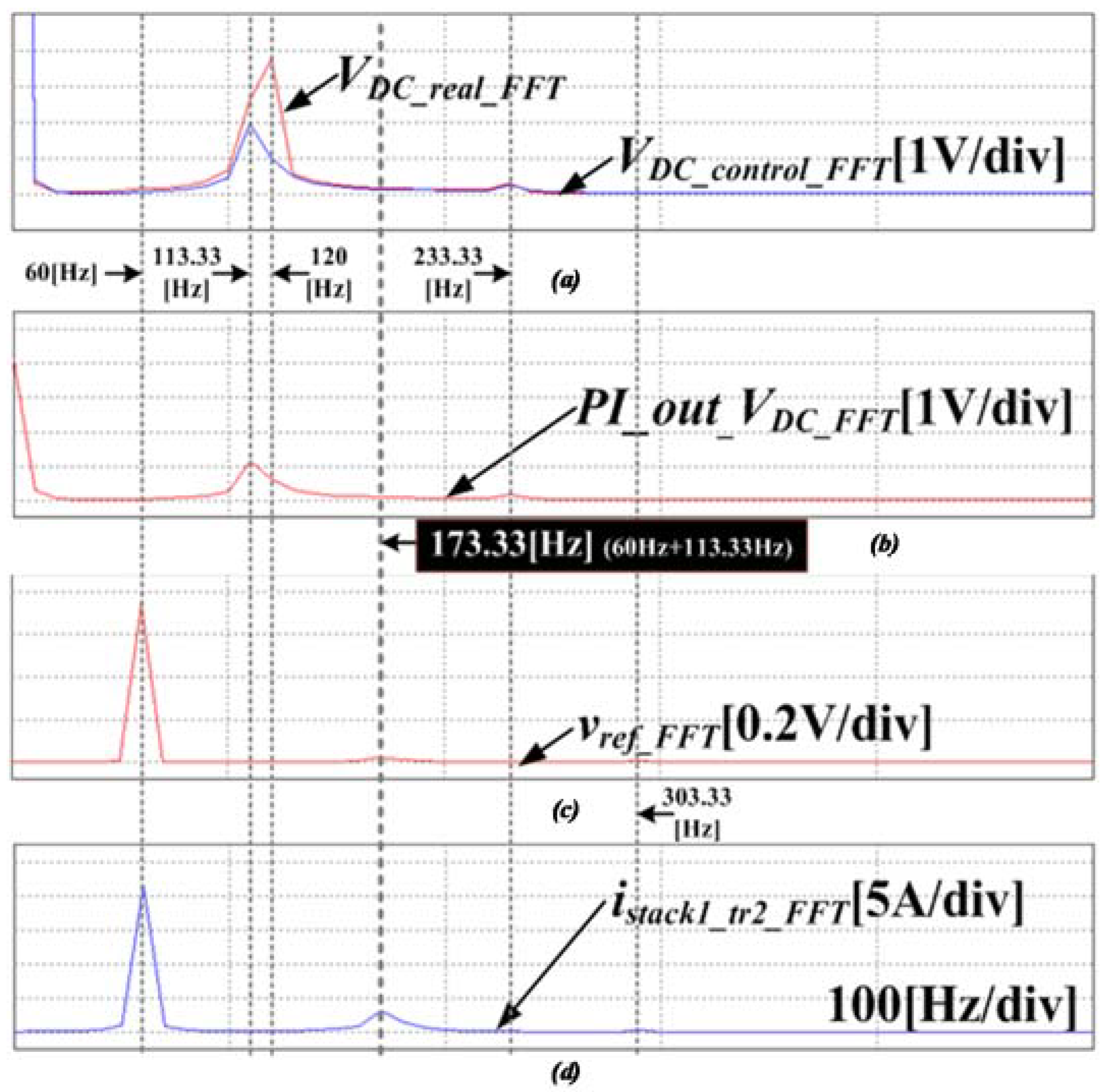
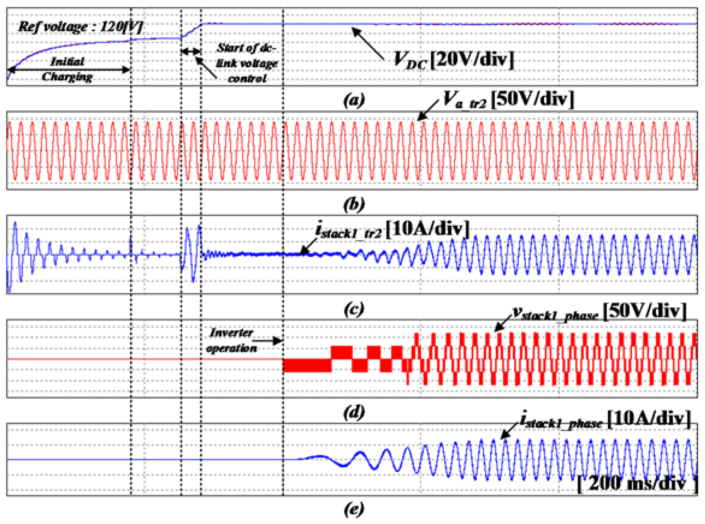
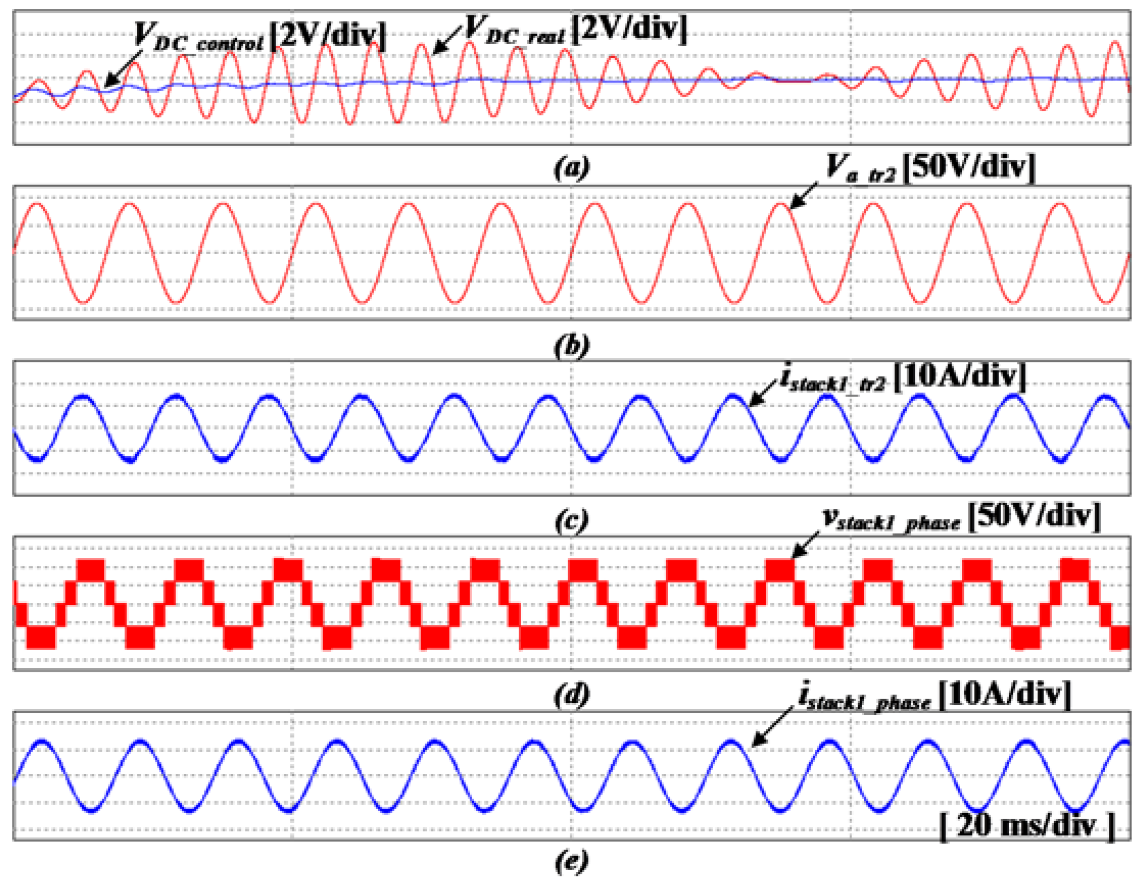
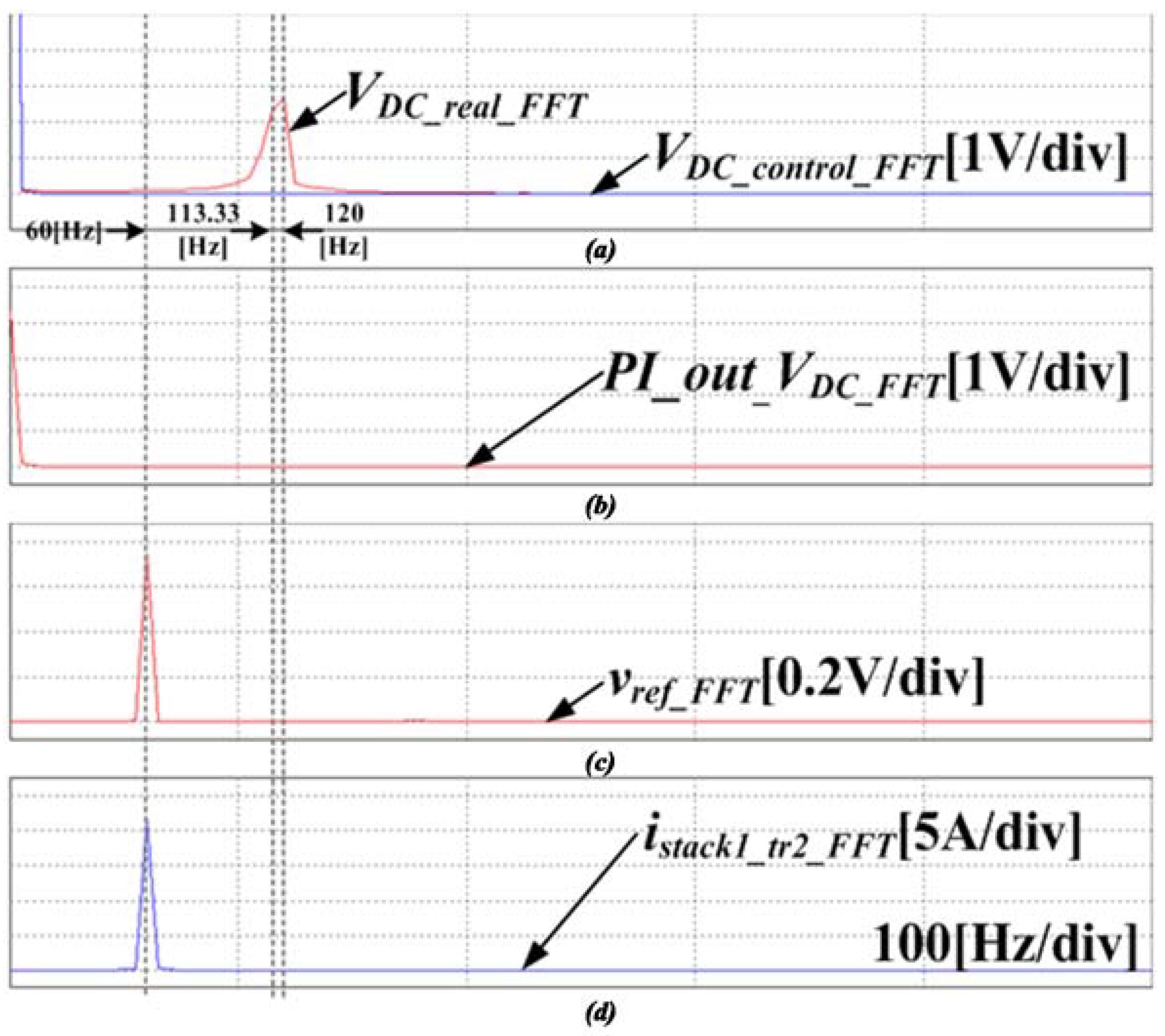
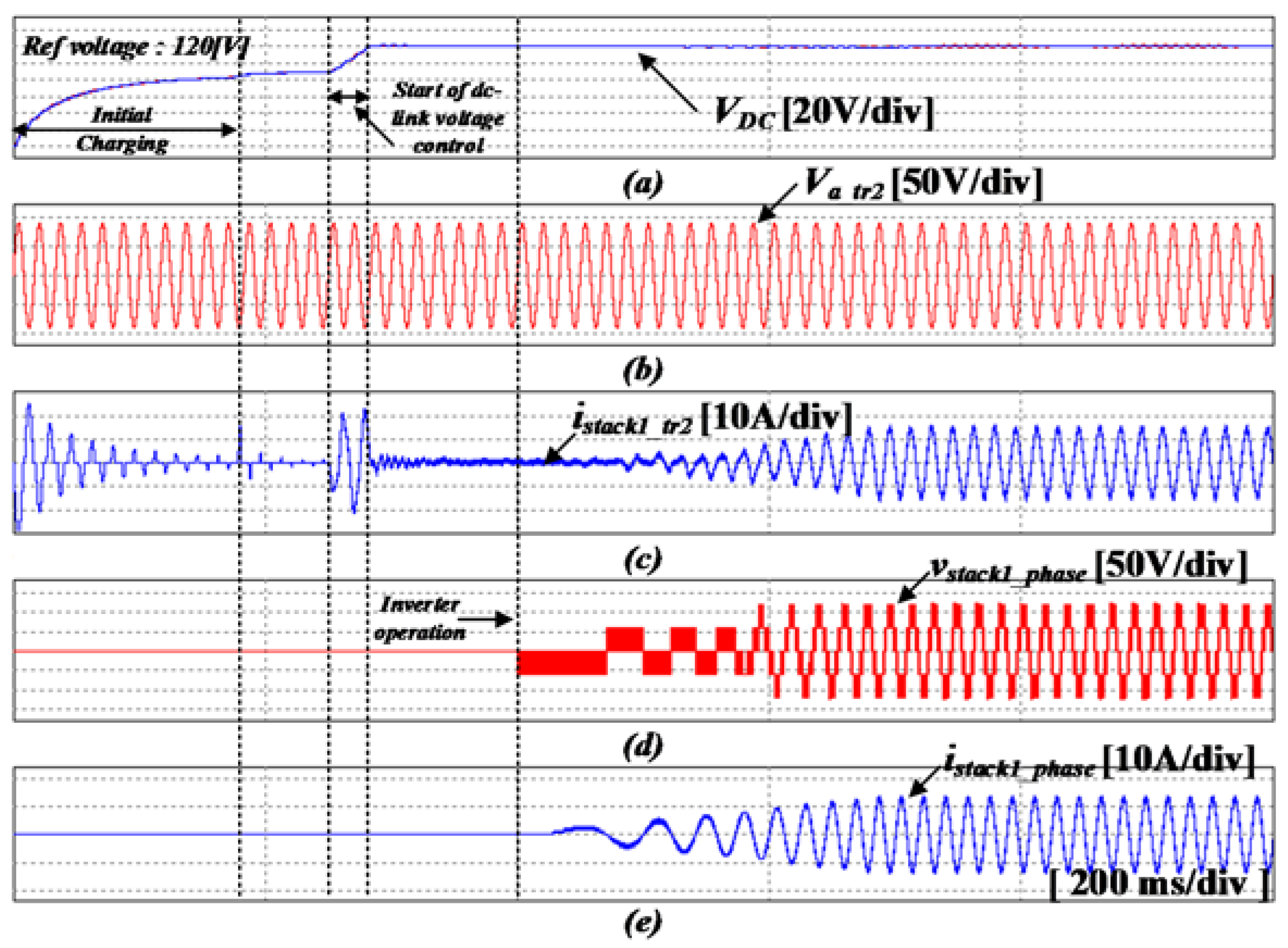
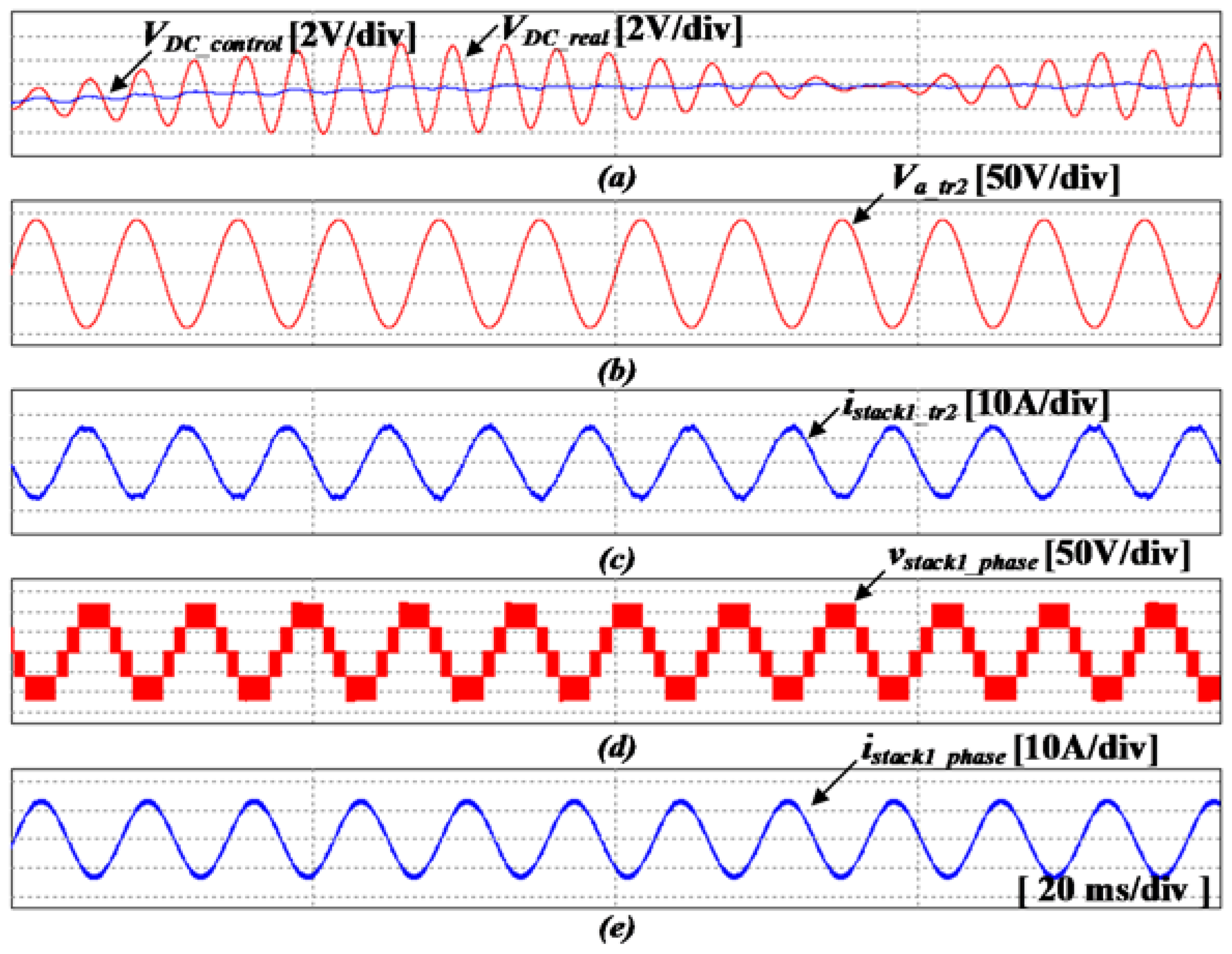
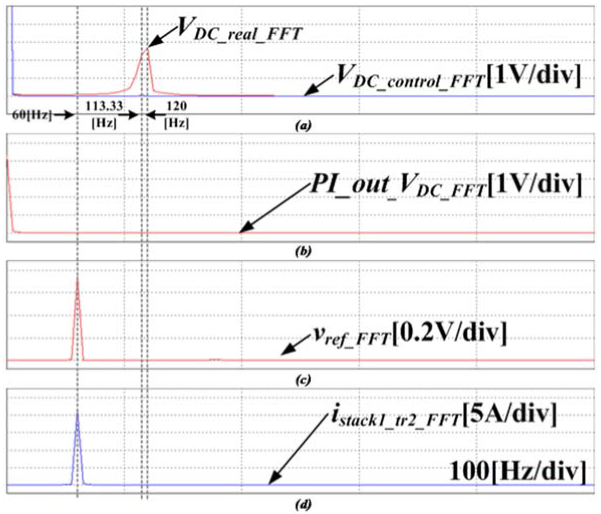
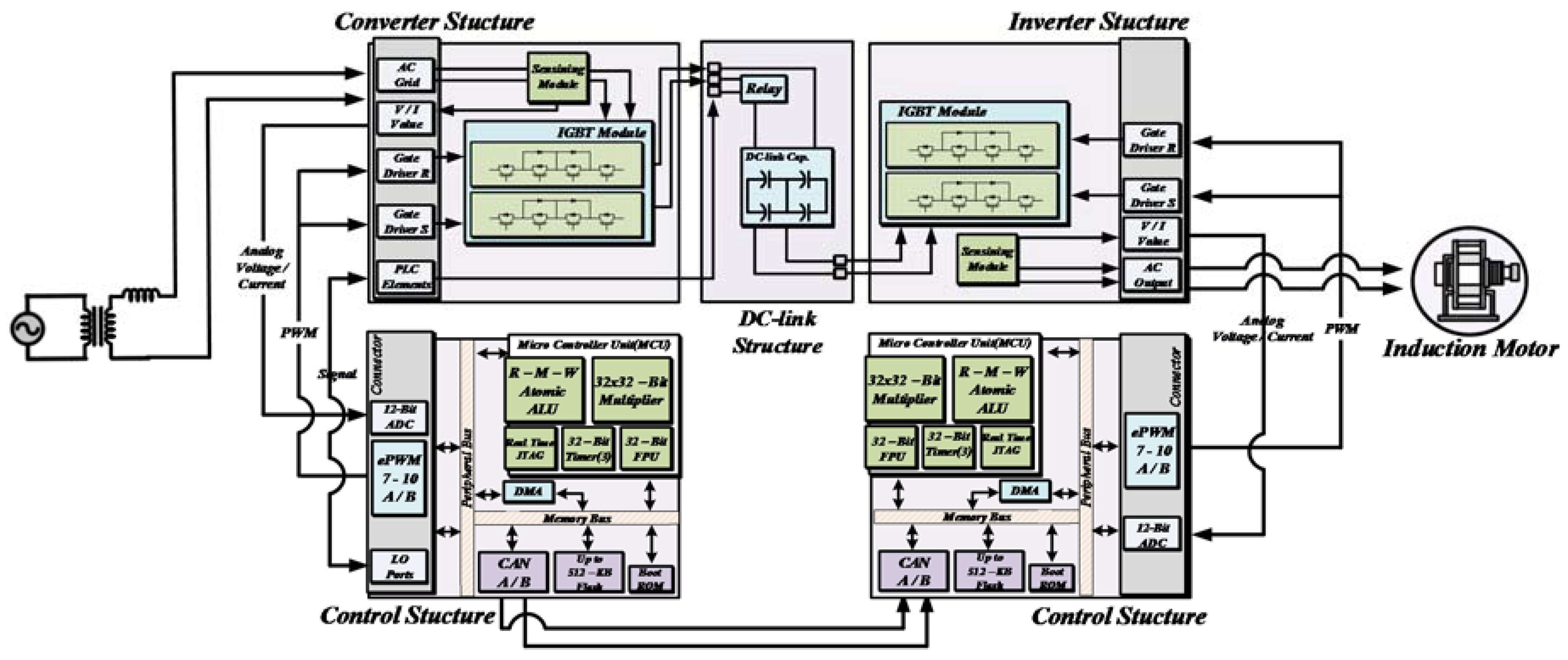
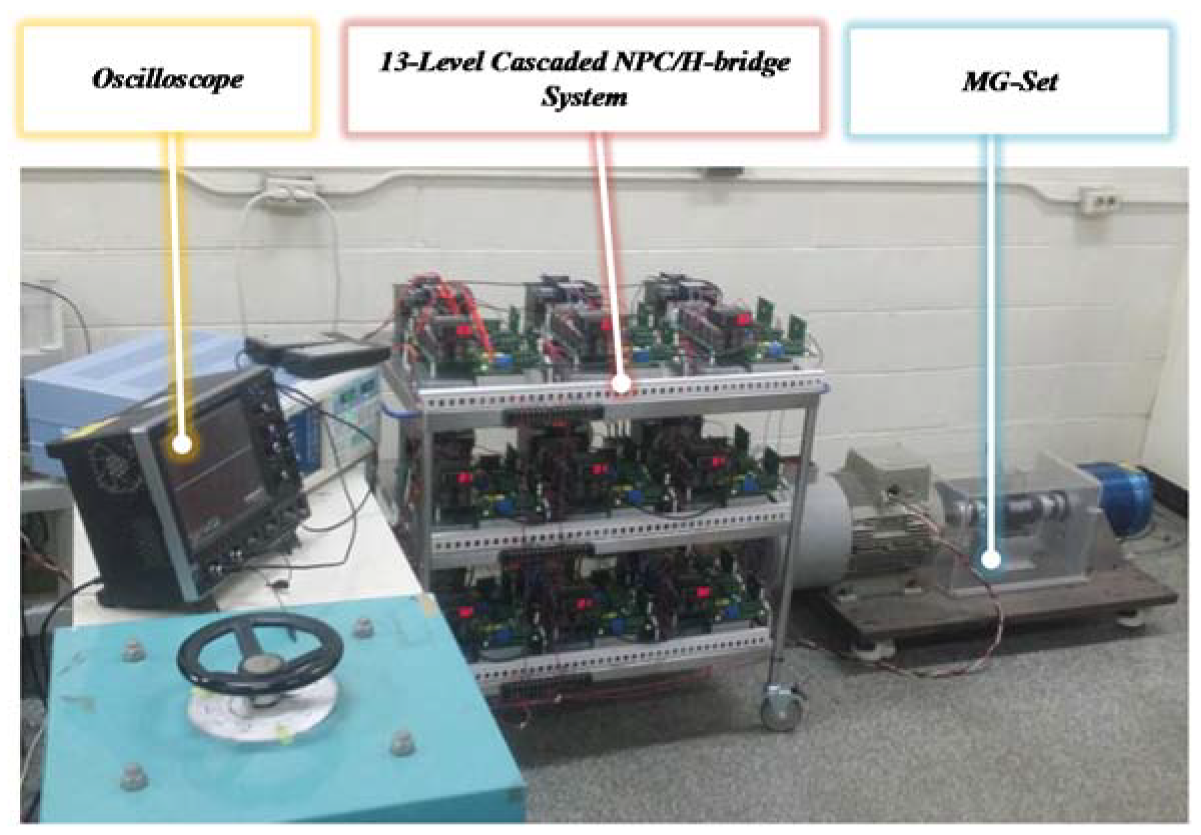
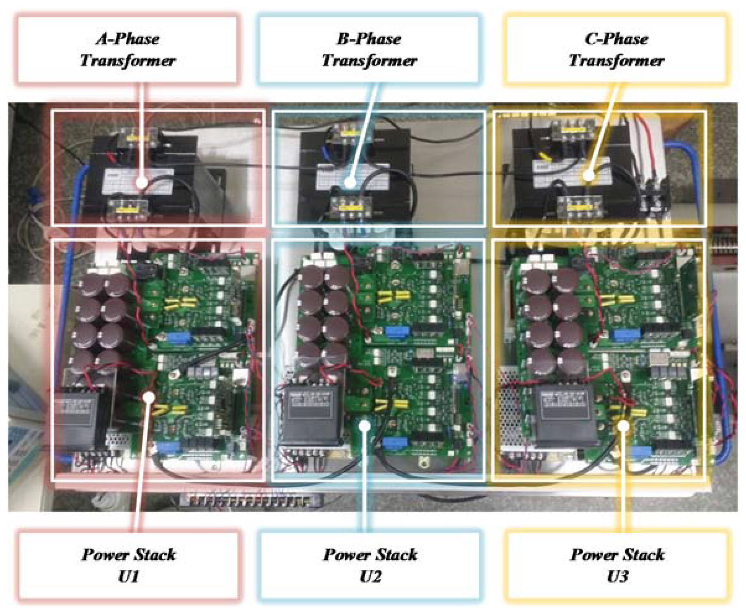
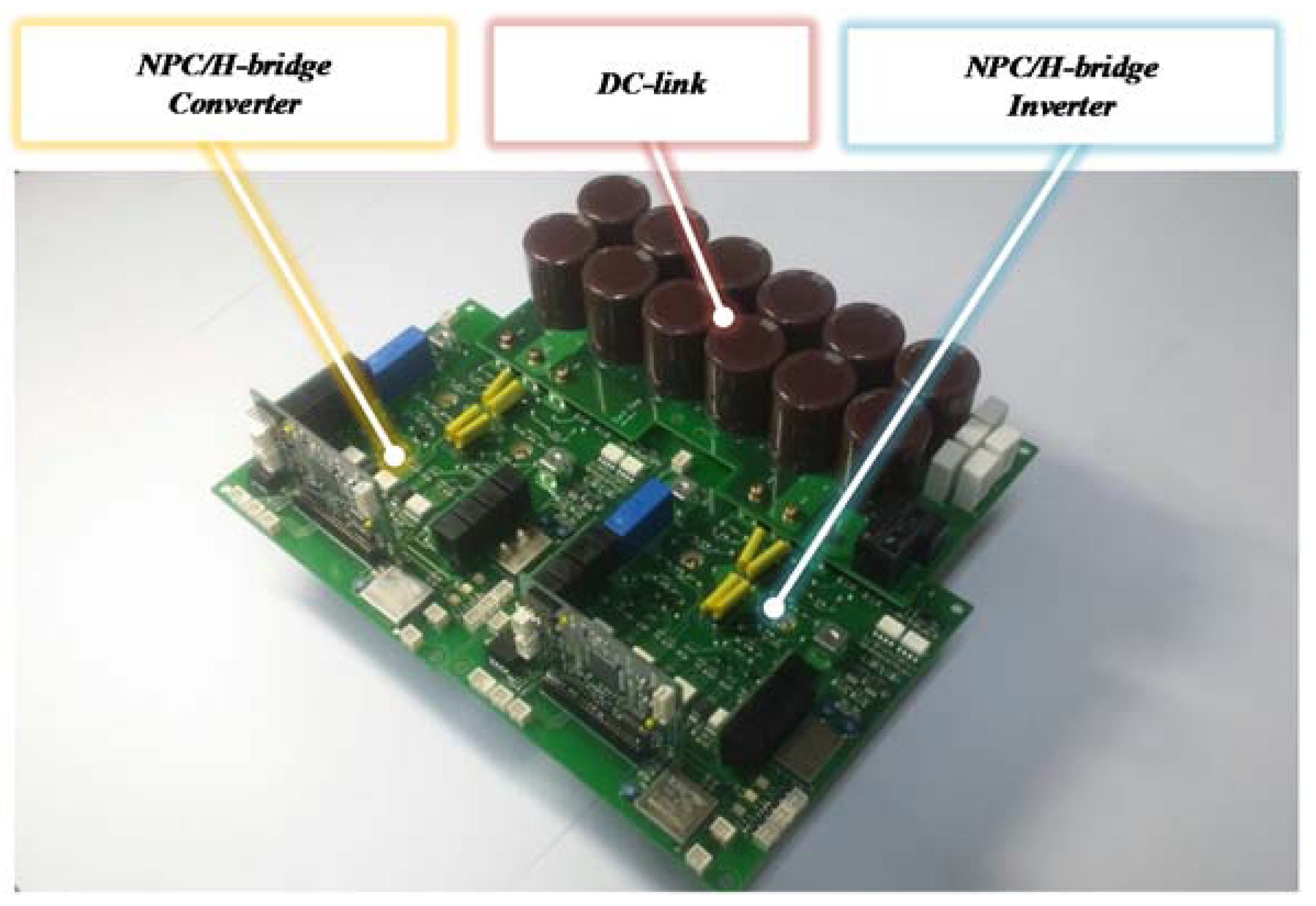
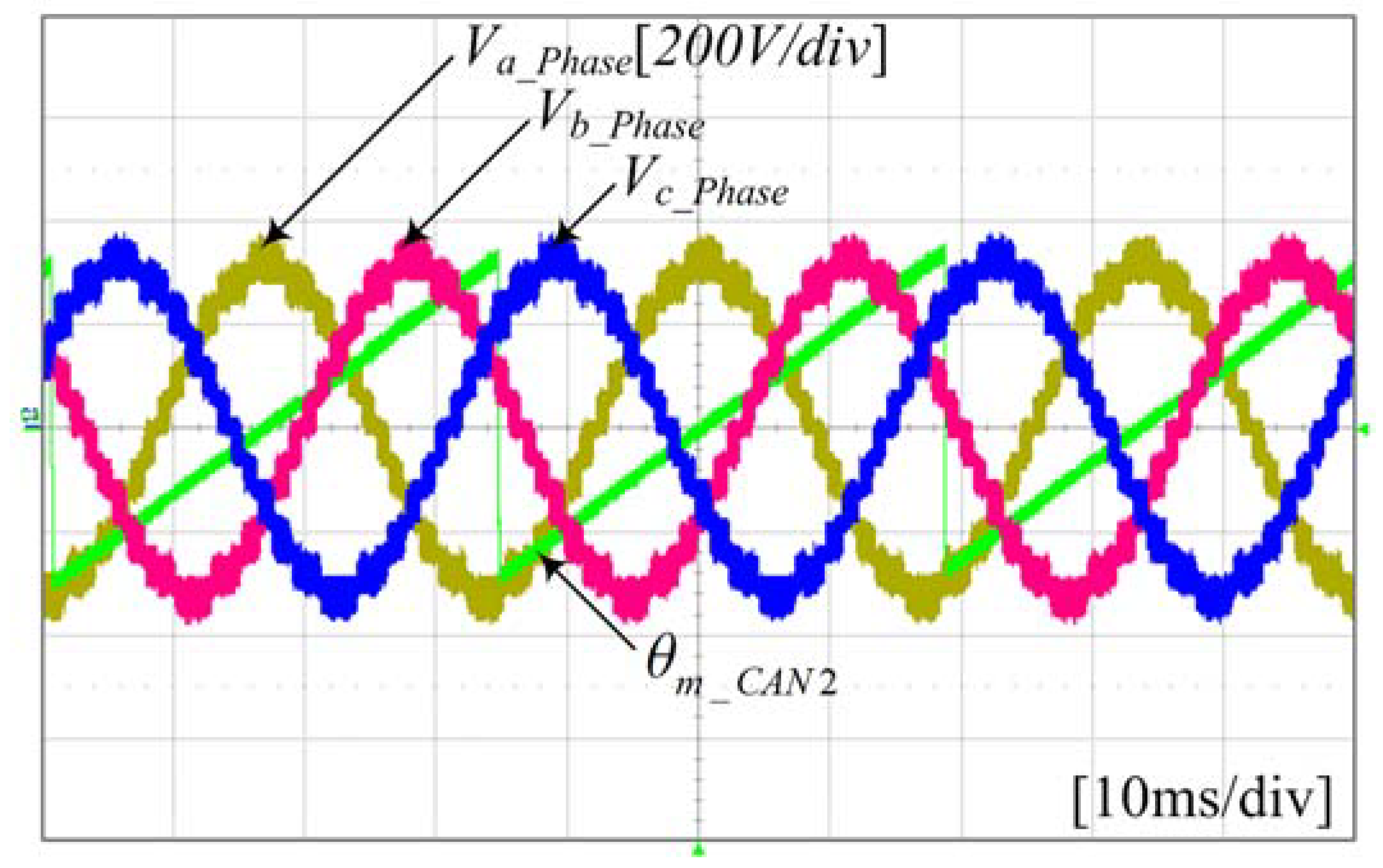
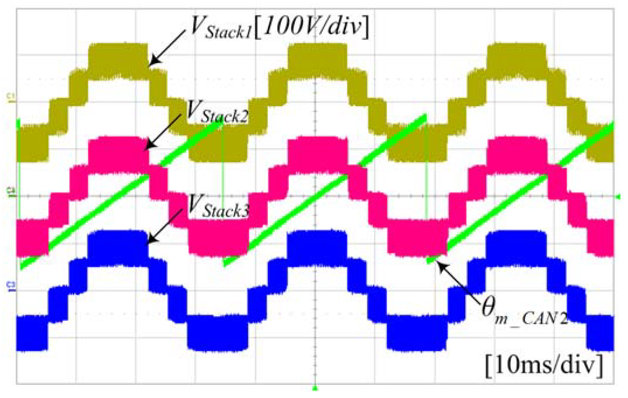
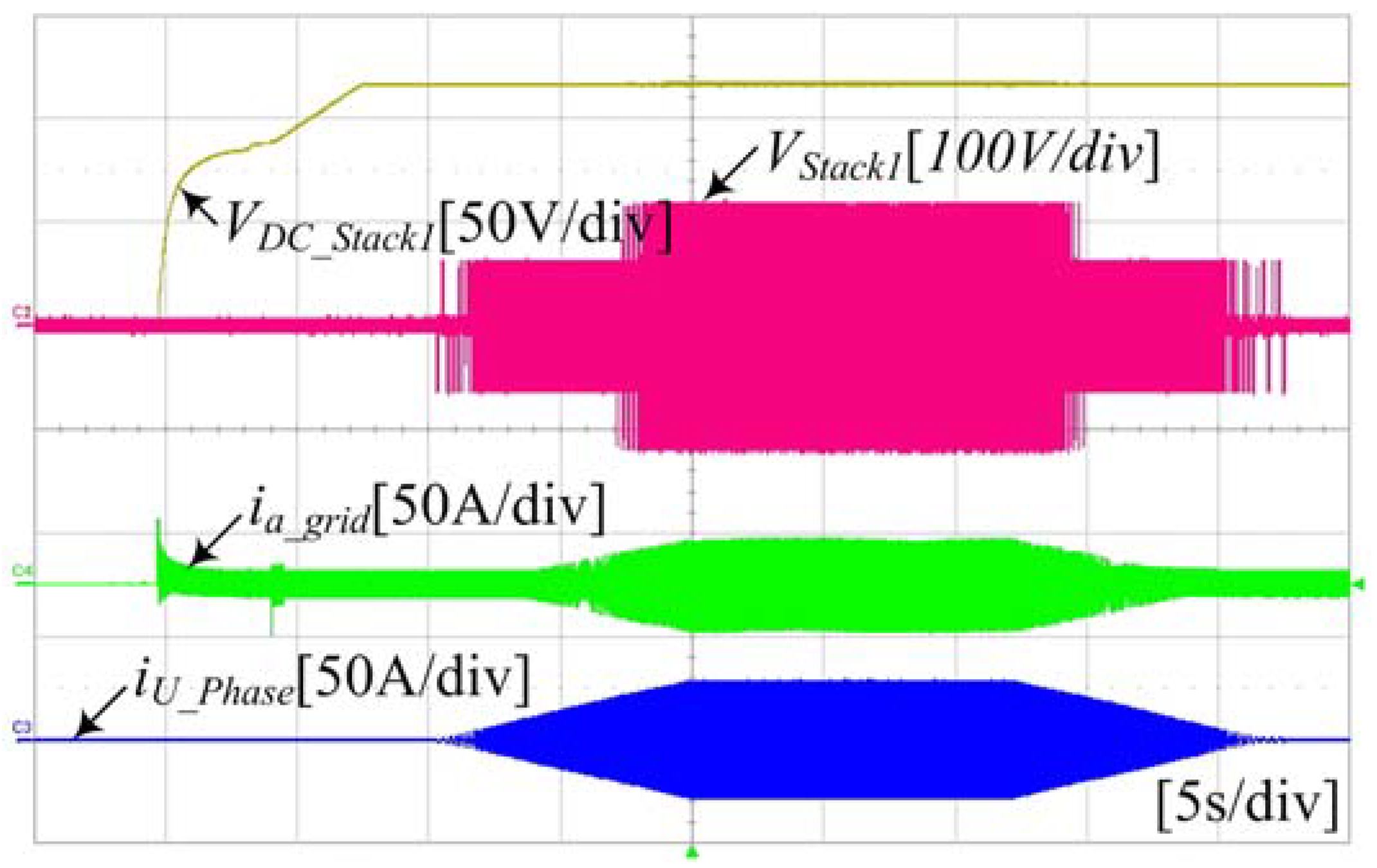
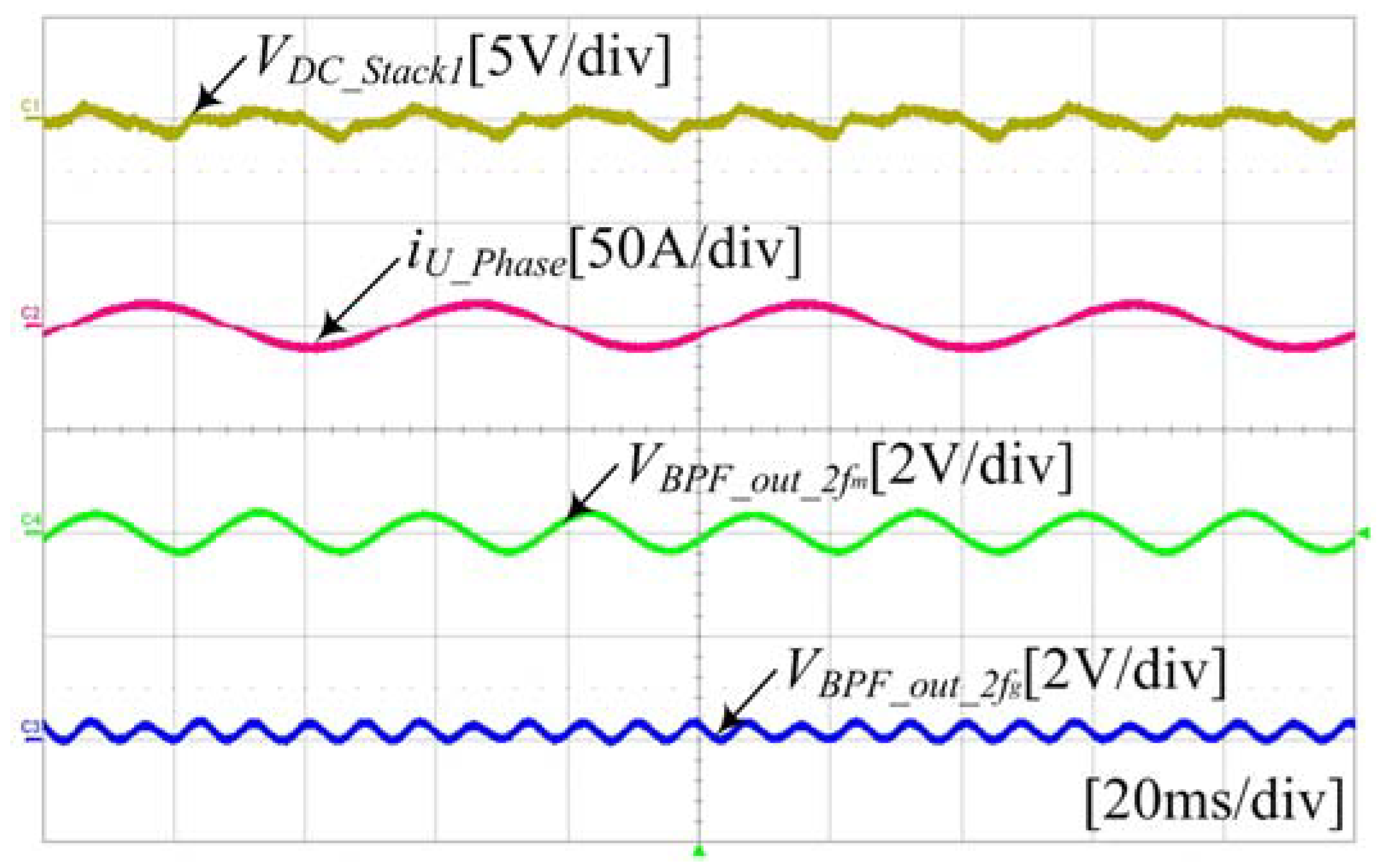
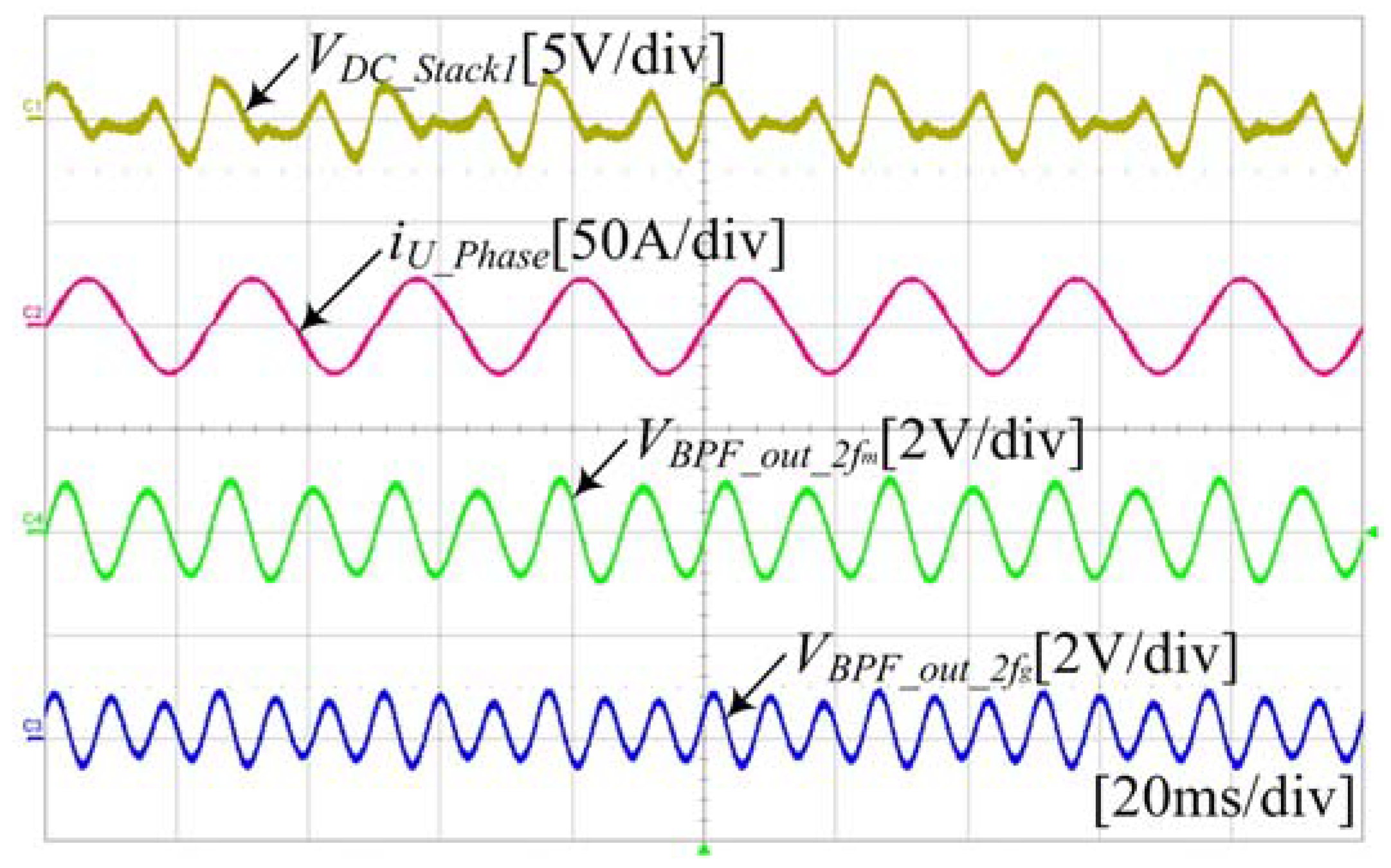
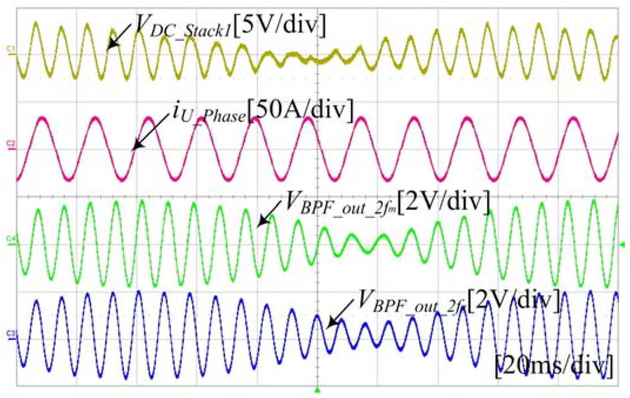
5. Experiment Results
6. Conclusions
Author Contributions
Acknowledgments
Conflicts of Interest
References
- Ying, J.; Gan, H. High power conversion technologies and trend. In Proceedings of the 2012 7th International Power Electronics and Motion Control Conference (IPEMC), Harbin, China, 2–5 June 2012; pp. 1766–1770. [Google Scholar]
- Marzoughi, A.; Burgos, R.; Boroyevich, D.; Xue, Y. Investigation and comparison of cascaded H-bridge and modular multilevel converter topologies for medium-voltage drive application. In Proceedings of the 40th Annual Conference of IEEE Industrial Electronics Society-IECON, Dallas, TX, USA, 29 October–1 November 2014; pp. 1562–1568. [Google Scholar]
- Qashqai, P.; Sheikholeslami, A.; Vahedi, H.; Al-Haddad, K. A review on multilevel converter topologies for electric transportation applications. In Proceedings of the IEEE-Vehicular Power and Propulsion Conference, Montréal, QC, Canada, 19–22 October 2015; pp. 1–6. [Google Scholar]
- Marzoughi, A.; Burgos, R.; Boroyevich, D.; Xue, Y. Design and Comparison of Cascaded H-Bridge, Modular Multilevel Converter, and 5-L Active Neutral Point Clamped Topologies for Motor Drive Applications. IEEE Trans. Ind. Appl. 2018, 54, 1404–1413. [Google Scholar] [CrossRef]
- Song, Z.; Tian, Y.; Yan, Z.; Chen, Z. Direct power control for three-phase two-level voltage-source rectifiers based on extended-state observation. IEEE Trans. Ind. Electron. 2016, 63, 4593–4603. [Google Scholar] [CrossRef]
- Hammond, P. A new approach to enhance power quality for medium voltage ac drives. IEEE Trans. Ind. Appl. 1997, 33, 202–208. [Google Scholar] [CrossRef]
- Sau, S.; Karmakar, S.; Fernandes, B.G. Modular Transformer-Based Regenerative-Cascaded Multicell Converter for Drives with Multilevel Voltage Operation at Both Input and Output Sides. IEEE Trans. Ind. Electron. 2018, 65, 5313–5323. [Google Scholar] [CrossRef]
- Malinowski, M.; Gopakumar, K.; Rodriguez, J.; Perez, M.A. A survey on cascaded multilevel inverters. IEEE Trans. Ind. Electron. 2010, 57, 2197–2206. [Google Scholar] [CrossRef]
- Ramírez, R.; Espinoza, J.; Baier, C. Operating region of a power cell in a CHB based topology operating at reduced second harmonic. In Proceedings of the 42nd Annual Conference of the IEEE Industrial Electronics Society, Florence, Italy, 23–26 October 2016; pp. 5058–5063. [Google Scholar]
- Liu, X.; Wang, P.; Loh, P.C.; Blaabjerg, F.; Xue, M. Six switches solution for single-phase AC/DC/AC converter with capability of second-order power mitigation in DC-link capacitor. In Proceedings of the Energy Conversion Congress and Exposition (ECCE), Phoenix, AZ, USA, 17–22 September 2011; pp. 1368–1375. [Google Scholar]
- Engel, S.P.; De Doncker, R.W. Control of the Modular Multi-Level Converter for minimized cell capacitance. In Proceedings of the 14th European Conference on Power Electronics and Applications (EPE 2011), Birmingham, UK, 30 August–1 September 2011; pp. 1–10. [Google Scholar]
- Kim, M.N.; Noh, Y.S.; Kim, J.G.; Jung, Y.C.; Won, C.Y. Active power decoupling using bi-directional resonant converter for flyback inverter without electrolytic capacitor of PV AC module system. In Proceedings of the International Conference on Electrical Machines and Systems, Busan, Korea, 26–29 October 2013; pp. 351–356. [Google Scholar]
- Zhu, G.R.; Tan, S.C.; Chen, Y.; Tse, C.K. Mitigation of Low-Frequency Current Ripple in Fuel-Cell Inverter Systems through Waveform Control. IEEE Trans. Power Electron. 2013, 28, 779–792. [Google Scholar] [CrossRef]
- Narayanasamy, B.; Luo, F.; Chu, Y. High density EMI mitigation solution using active approaches. In Proceedings of the IEEE International Symposium on Electromagnetic Compatibility & Signal/Power Integrity (EMCSI 2017), Washington, DC, USA, 7–11 August 2017; pp. 813–818. [Google Scholar]
- Zhao, H.; Wang, S.; Moeini, A.; Yang, L. Investigation of CCL filter for multilevel selective compensation (SHC) with staircase modulation. In Proceedings of the IEEE Energy Conversion Congress and Exposition (ECCE), Cincinnati, OH, USA, 1–5 October 2017; pp. 5206–5213. [Google Scholar]
- Peña-Alzola, R.; Campos-Gaona, D.; Ksiazek, P.F.; Ordonez, M. DC-Link Control Filtering Options for Torque Ripple Reduction in Low-Power Wind Turbines. IEEE Trans. Power Electron. 2017, 32, 4812–4826. [Google Scholar] [CrossRef]
- Sha, D.; Xu, Y.; Zhang, J.; Yan, Y. Current-Fed Hybrid Dual Active Bridge DC–DC Converter for a Fuel Cell Power Conditioning System with Reduced Input Current Ripple. IEEE Trans. Ind. Electron. 2017, 64, 6628–6638. [Google Scholar] [CrossRef]
- Zhao, W.; Ruan, X.; Yang, D.; Chen, X.; Jia, L. Neutral Point Voltage Ripple Suppression for a Three-Phase Four-Wire Inverter with an Independently Controlled Neutral Module. IEEE Trans. Ind. Electron. 2017, 64, 2608–2619. [Google Scholar] [CrossRef]
- Ghartemani, M.K.; Khajehoddin, S.A.; Jain, P.K.; Bakhshai, A.; Mojiri, M. Addressing DC component in PLL and notch filter algorithms. IEEE Trans. Power Electron. 2012, 27, 78–86. [Google Scholar] [CrossRef]
- Trinh, Q.N.; Wang, P.; Tang, Y.L.; Koh, H.; Choo, F.H. Compensation of DC Offset and Scaling Errors in Voltage and Current Measurements of Three-Phase AC/DC Converters. IEEE Trans. Power Electron. 2018, 33, 5401–5414. [Google Scholar] [CrossRef]
- Karimi-Ghartemani, M.; Mojiri, M.; Safaee, A.; Walseth, J.A.; Khajehoddin, S.A.; Jain, P.; Bakhshai, A. A New Phase-Locked Loop System for Three-Phase Applications. IEEE Trans. Power Electron. 2013, 28, 1208–1218. [Google Scholar] [CrossRef]
- Wu, F.; Sun, D.; Duan, J. Diagnosis of single-phase open-line fault in three-phase PWM rectifier with LCL filter. IET Gener. Trans. Distrib. 2016, 10, 1410–1421. [Google Scholar] [CrossRef]
- Hansen, A.D.; Michalke, G. Modelling and control of variable-speed multi-pole permanent magnet synchronous generator wind turbine. Wind Energy 2008, 11, 537–554. [Google Scholar] [CrossRef]
- Zhu, C.; Zeng, Z.; Zhao, R. Adaptive suppression method for DC-link voltage offset in three-phase four-switch inverter-fed PMSM drives. IET Electron. Lett. 2016, 52, 1442–1444. [Google Scholar] [CrossRef]
- Zhao, Z. Adaptive internal model control based ripple rejection for improved response of PFC rectifiers. In Proceedings of the 30th Annual Conference on Electrical and Computer Engineering (CCECE 2017), Windsor, ON, USA, 30 April–3 May 2017; pp. 1–6. [Google Scholar]
- El-Naga, A.A.A.; Marei, M.I.; El-Goharey, H.S.K. Second order adaptive notch filter based wind power smoothing using flywheel energy storage system. In Proceedings of the 19th International Middle East Power Systems Conference (MEPCON), Nasr City, EG, USA, 19–21 December 2017; pp. 314–319. [Google Scholar]
- Kang, J.W.; Hyun, S.W.; Park, W.H.; Lee, H.; Won, C.W. Advanced Control Method for Reduction of DC-Link Ripple in Cascaded NPC/H-bridge System. In Proceedings of the 23rd International Conference on Electrical Engineering, Weihai, China, 4–7 July 2017; pp. 1421–1426. [Google Scholar]
- Lezana, P.; Rodriguez, J.; Oyarzun, D.A. Cascaded Multilevel Inverter with Regeneration Capability and Reduced Number of Switches. IEEE Trans. Ind. Electron. 2008, 55, 1059–1066. [Google Scholar] [CrossRef]
- Xinghua, T.; Yongdong, L.; Min, S. A phase-disposition PWM method for DC voltage balance in cascaded H-Bridge rectifier. In Proceedings of the 2010 International Conference on Electrical Machines and Systems (ICEMS 2010), Incheon, Korea, 10–13 October 2010; pp. 243–248. [Google Scholar]


| Parameter | Value | Unit | Parameter | Value | Unit |
|---|---|---|---|---|---|
| Rated power of transformer | 1.1 | kW | Input voltage of each stack | 89 | V |
| Turn ratio | 2:1 | turn | Filter inductance | 1 | |
| Rated power | 15 | kW | Switching frequency | 10 | kHz |
| Rated voltage | 380 | Vrms | DC-link voltage | 120 | V |
| Rated current | 27.8 | Arms | DC-link capacitance | 4 | |
| Rated power of each stack | 1.1 | kW |
| Control Method | [V] | [V] | [V] | THD [%] | Power Factor |
|---|---|---|---|---|---|
| Conventional NF | 126.1 | 114.6 | 11.4 | 17.03 | 0.98 |
| Proposed SNF | 125.4 | 114.5 | 10.9 | 2.38 | 0.99 |
| Proposed DBPF | 125.4 | 114.5 | 10.9 | 2.36 | 0.99 |
© 2018 by the authors. Licensee MDPI, Basel, Switzerland. This article is an open access article distributed under the terms and conditions of the Creative Commons Attribution (CC BY) license (http://creativecommons.org/licenses/by/4.0/).
Share and Cite
Kang, J.-W.; Lee, H.; Hyun, S.-W.; Kim, J.; Won, C.-Y. An Enhanced Control Scheme Based on New Adaptive Filters for Cascaded NPC/H-Bridge System. Energies 2018, 11, 1034. https://doi.org/10.3390/en11051034
Kang J-W, Lee H, Hyun S-W, Kim J, Won C-Y. An Enhanced Control Scheme Based on New Adaptive Filters for Cascaded NPC/H-Bridge System. Energies. 2018; 11(5):1034. https://doi.org/10.3390/en11051034
Chicago/Turabian StyleKang, Jin-Wook, Hoon Lee, Seung-Wook Hyun, Jintae Kim, and Chung-Yuen Won. 2018. "An Enhanced Control Scheme Based on New Adaptive Filters for Cascaded NPC/H-Bridge System" Energies 11, no. 5: 1034. https://doi.org/10.3390/en11051034
APA StyleKang, J.-W., Lee, H., Hyun, S.-W., Kim, J., & Won, C.-Y. (2018). An Enhanced Control Scheme Based on New Adaptive Filters for Cascaded NPC/H-Bridge System. Energies, 11(5), 1034. https://doi.org/10.3390/en11051034