An Original Transformer and Switched-Capacitor (T & SC)-Based Extension for DC-DC Boost Converter for High-Voltage/Low-Current Renewable Energy Applications: Hardware Implementation of a New T & SC Boost Converter

 ,
,  ,
, 
 and
and
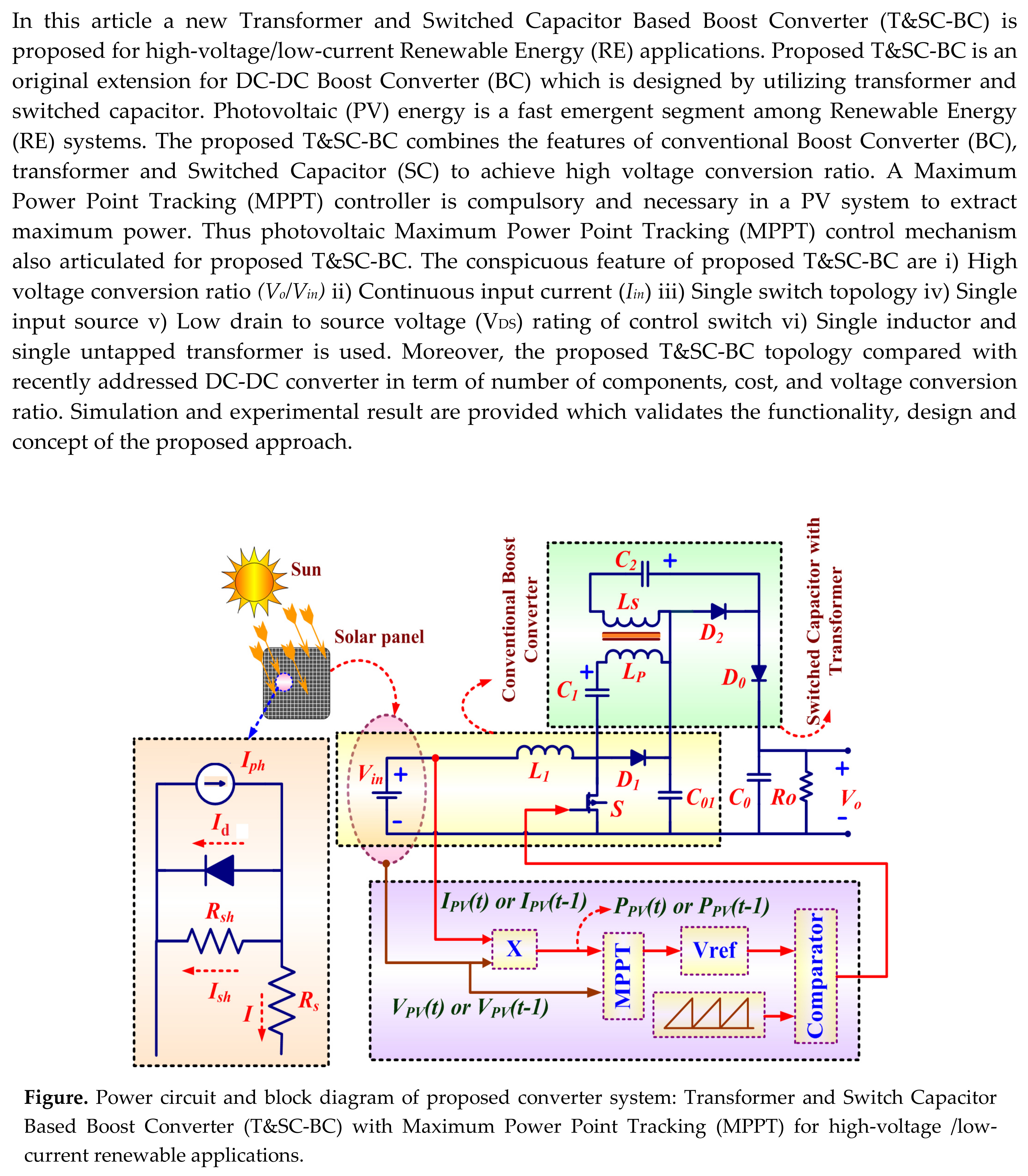
Abstract
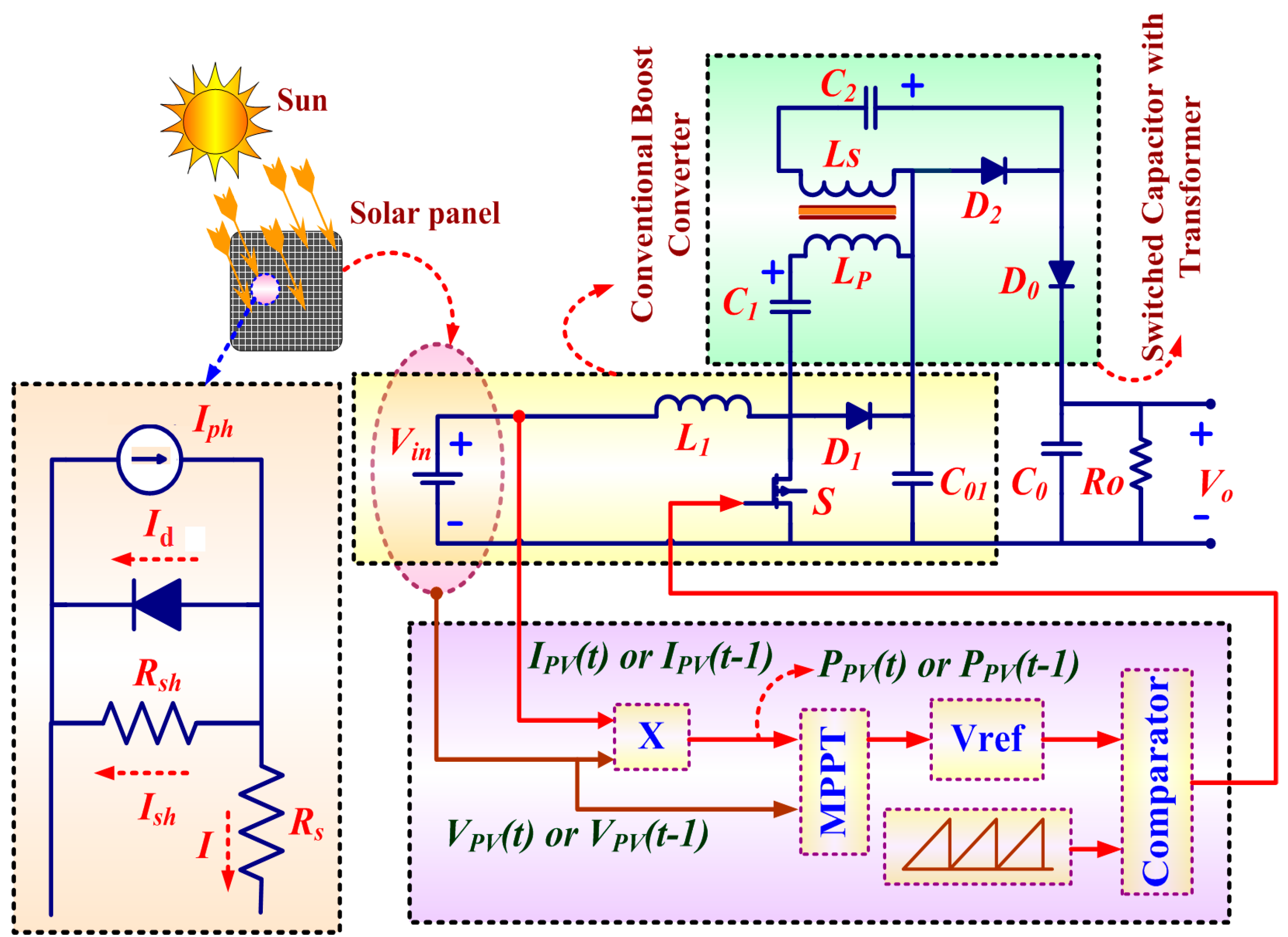
: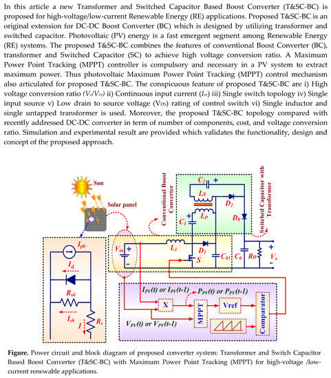
1. Introduction
- (1)
- High voltage conversion ratio (Vo/Vin),
- (2)
- Continuous input current (Iin),
- (3)
- Single switch topology,
- (4)
- Single input source,
- (5)
- Low Drain to Source voltage (VDS) rating of switch,
- (6)
- Single inductor and single untapped transformer.
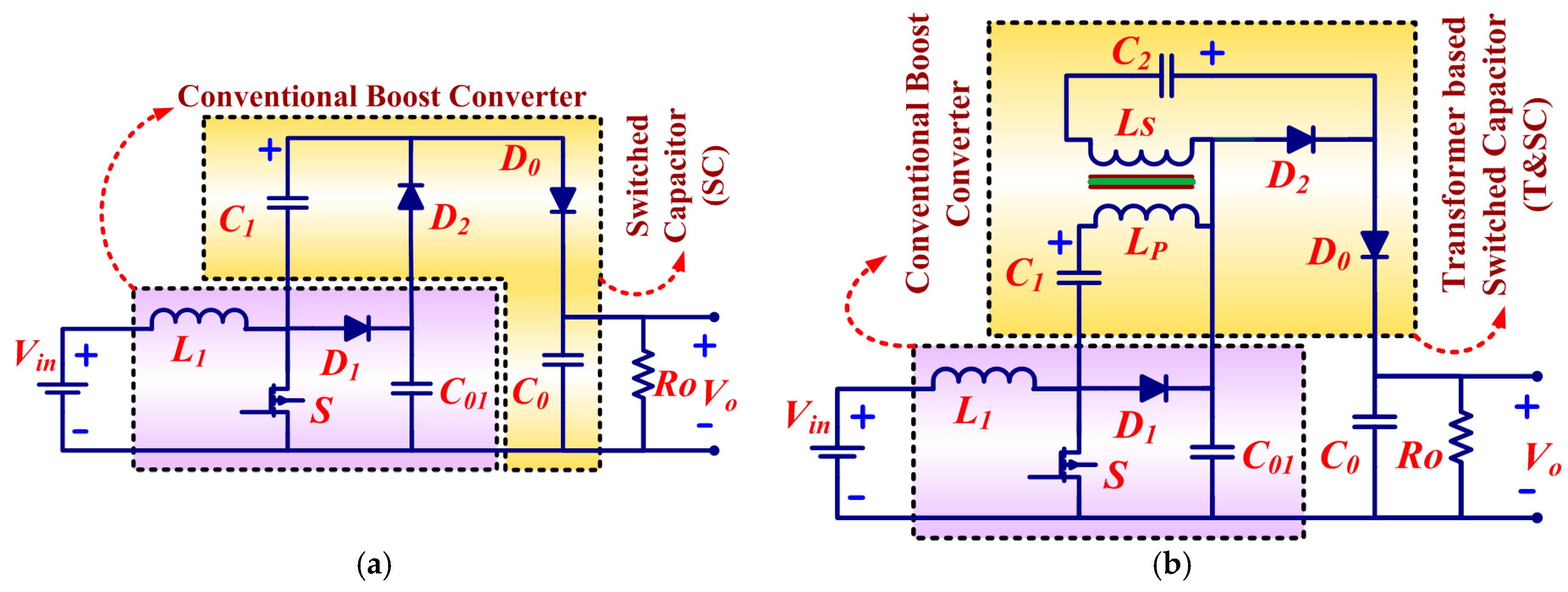
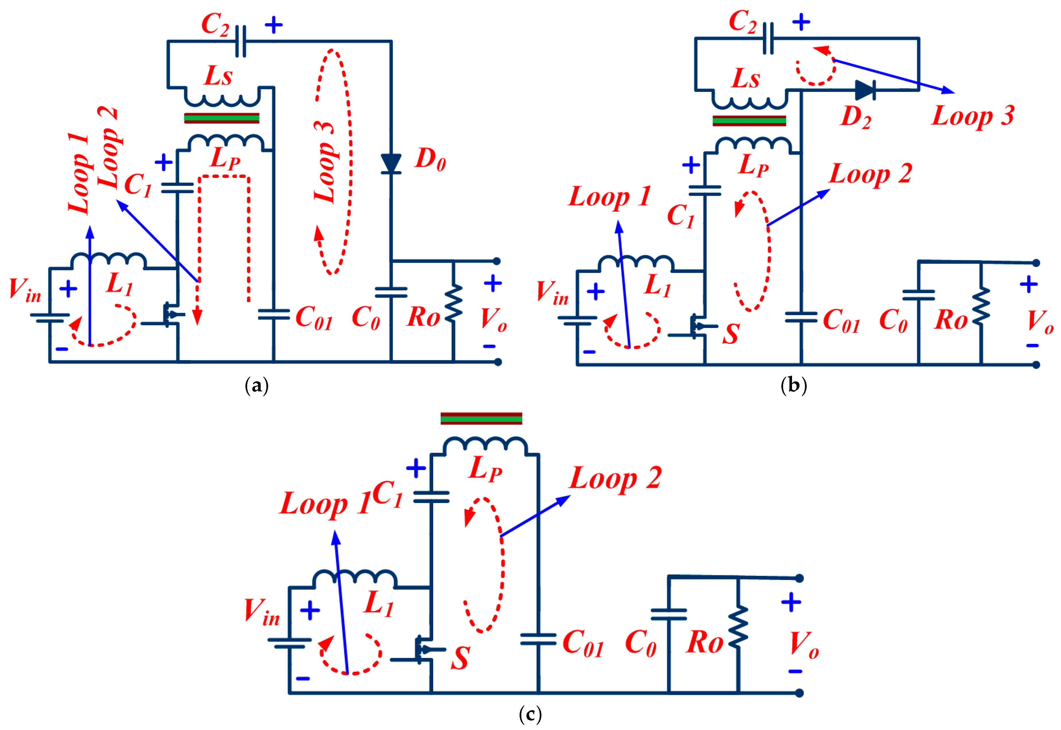
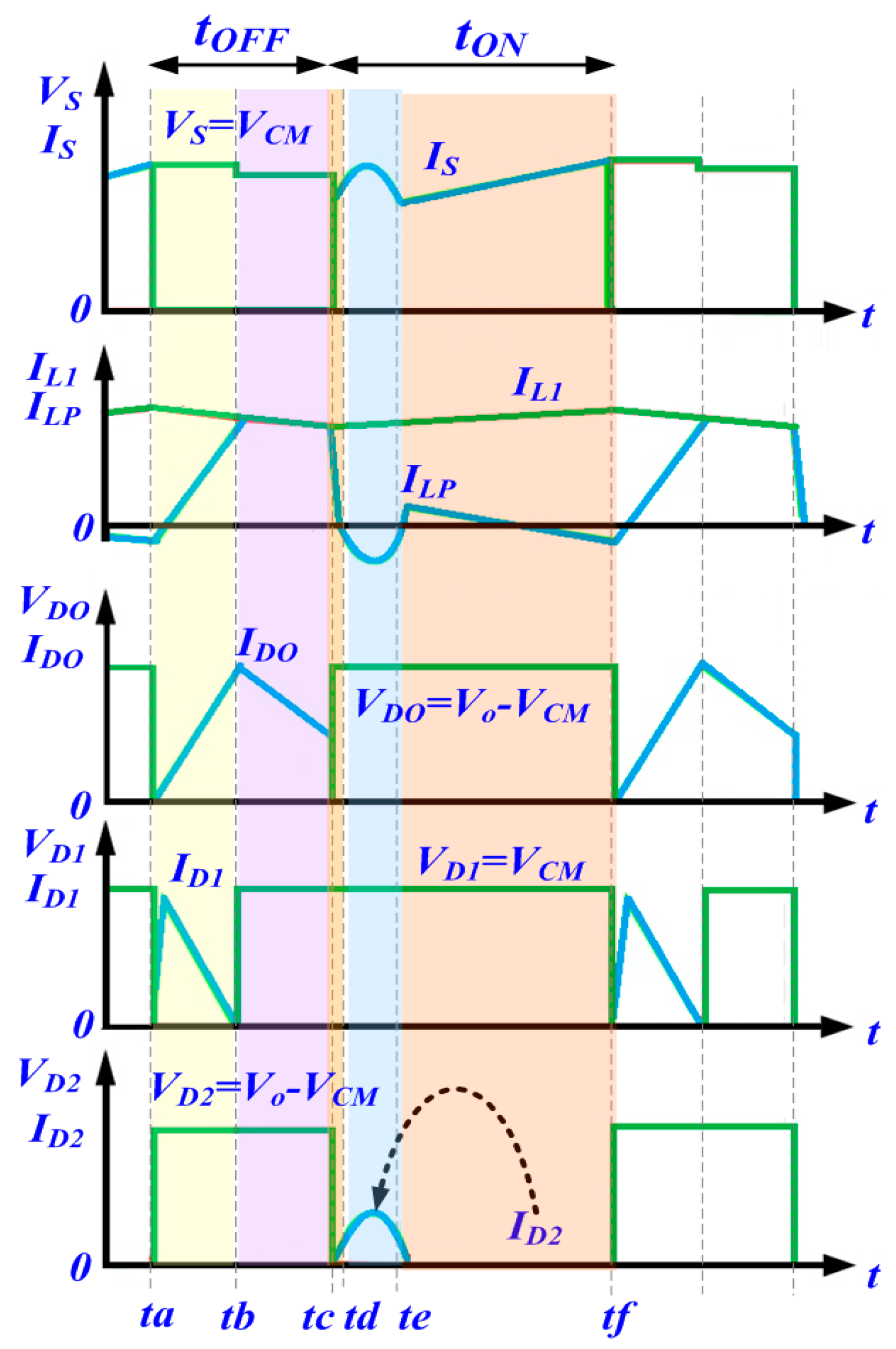
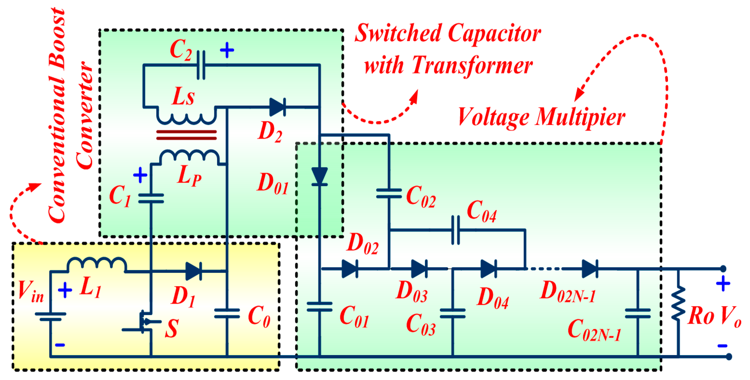
2. Power Circuit and Operation Modes of Transformer and Switch Capacitor Based Boost Converter (T & SC-BC)
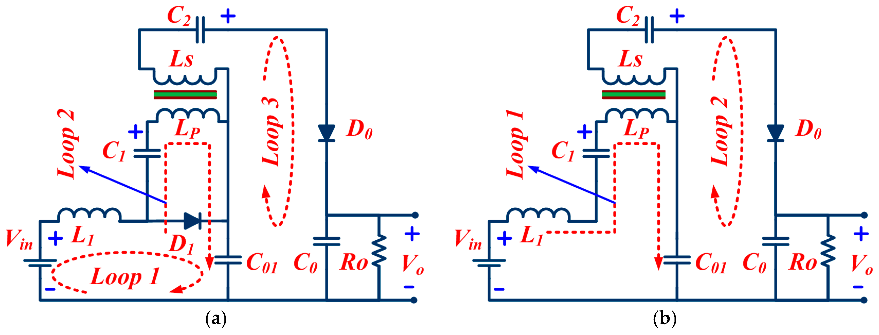
2.1. Mode-1 (Time ta–tb)
2.2. Mode-2 (Time tb–tc)
2.3. Mode-3 (Time tc–td)
2.4. Mode-4 (Time td–te)
2.5. Mode-5 (Time te–tf)
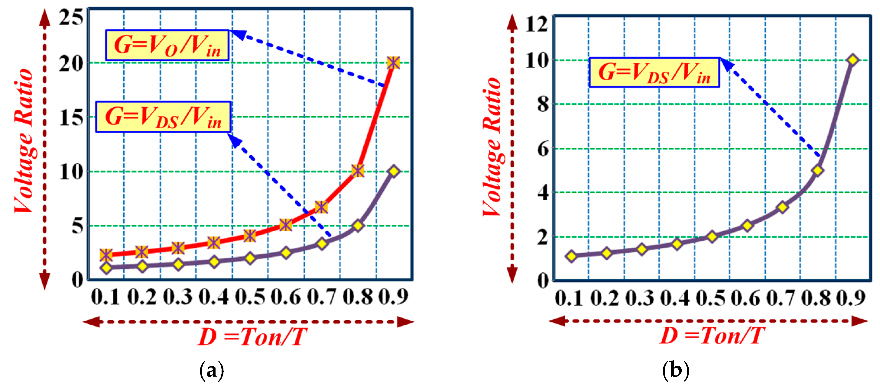
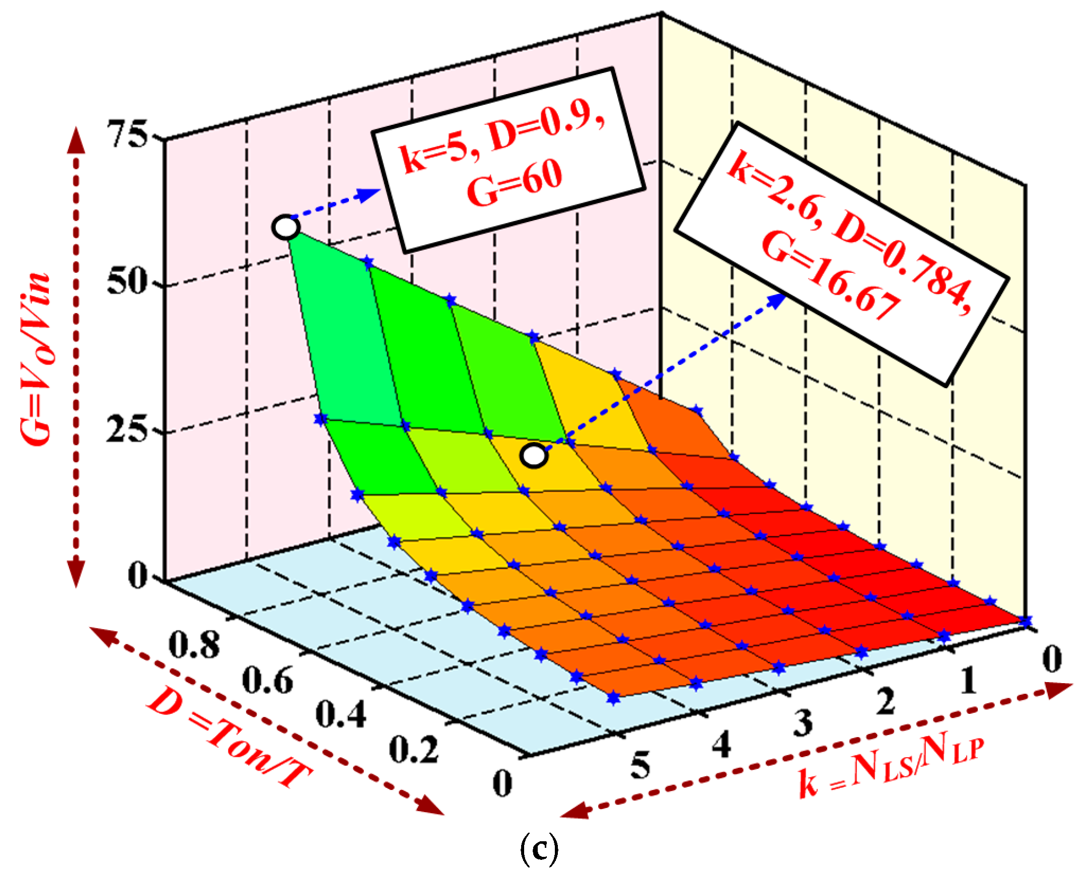
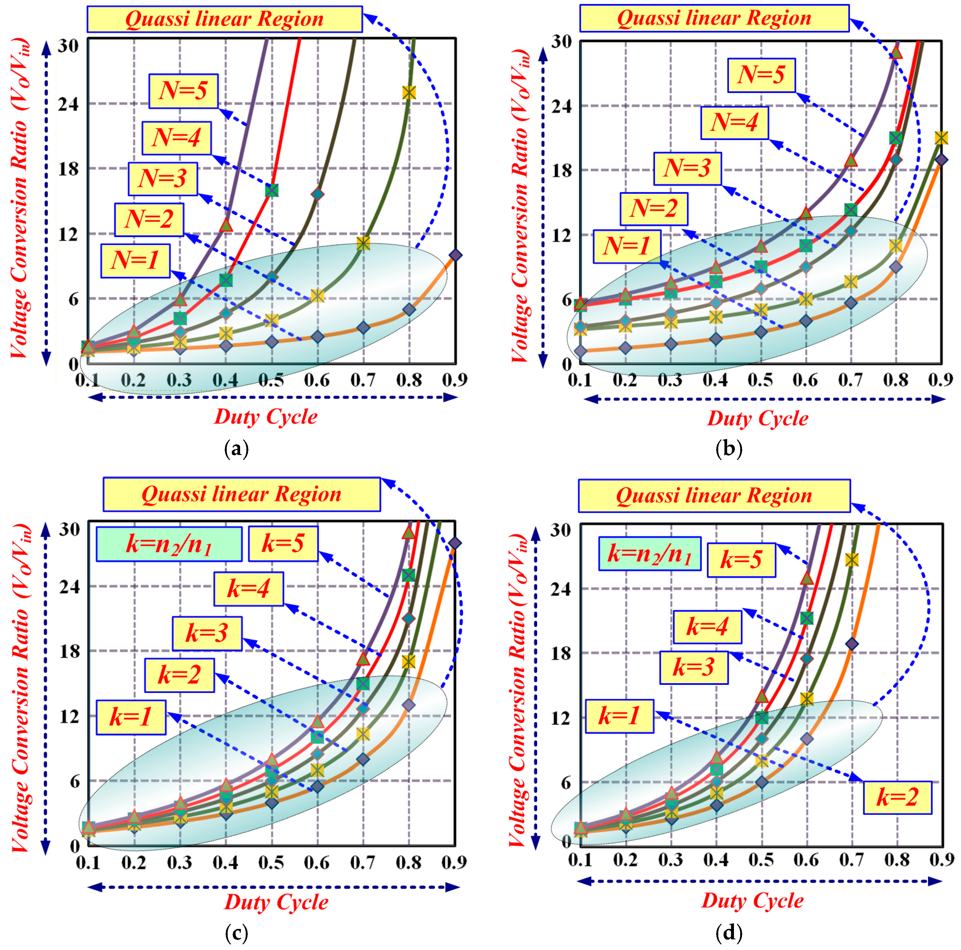
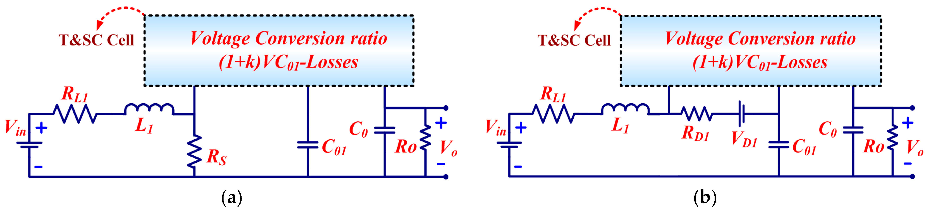
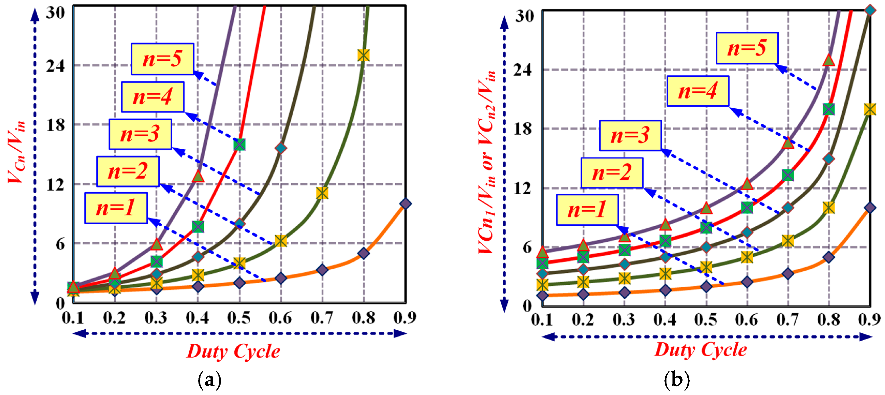
3. Steady State Analysis of Transformer and Switch Capacitor Based Boost Converter (T & SC-BC)
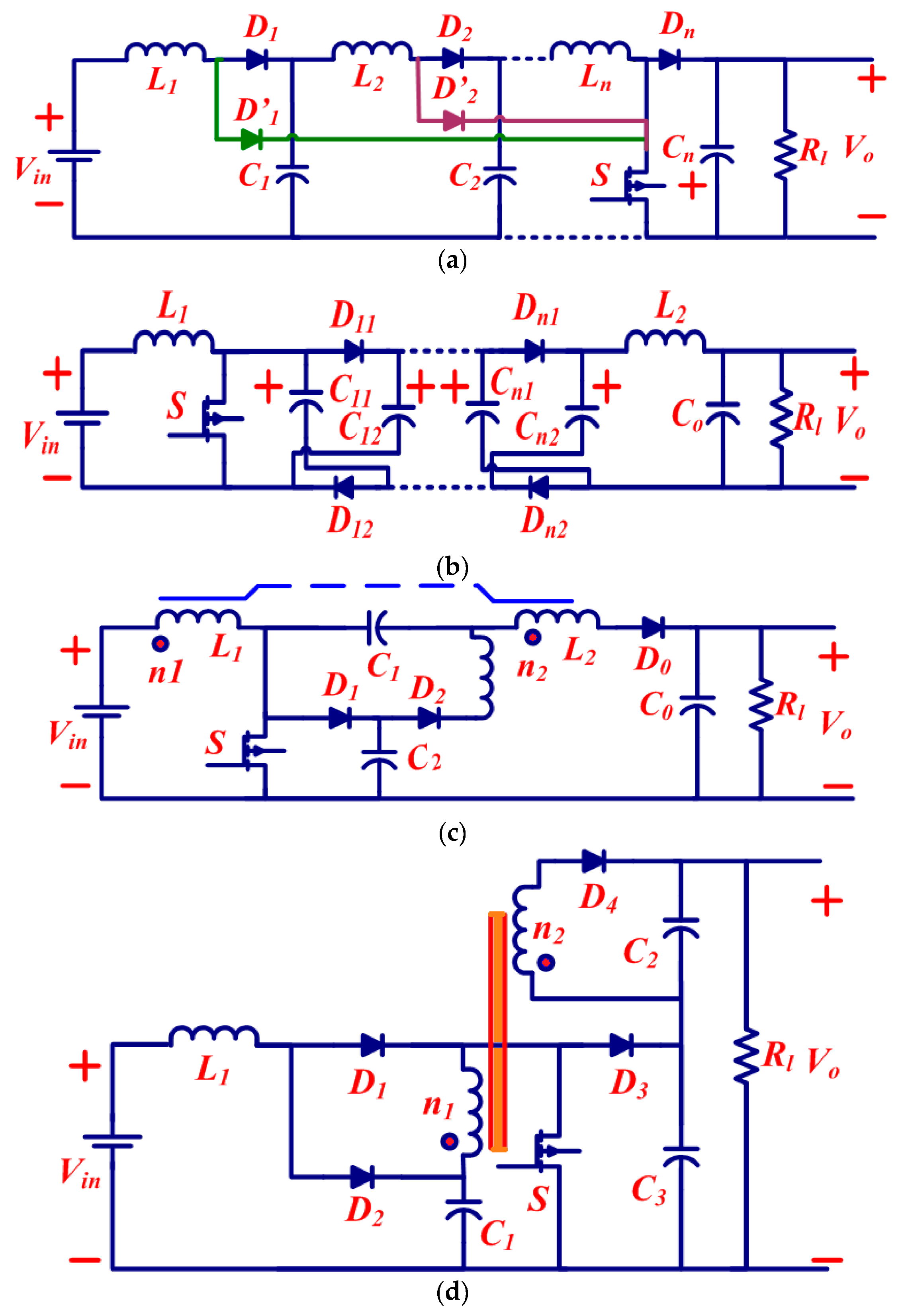
4. Comparison of Proposed Transformer and Switch Capacitor Based Boost Converter (T & SC-BC) with Newly Addressed DC-DC Converters
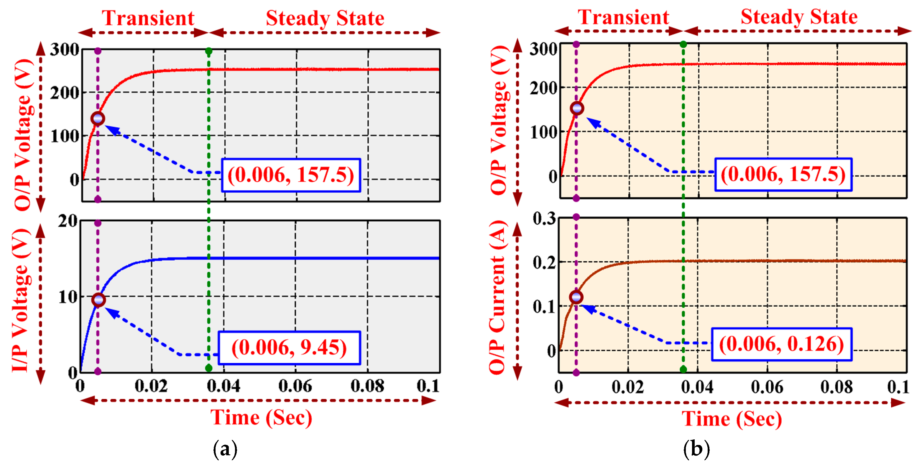
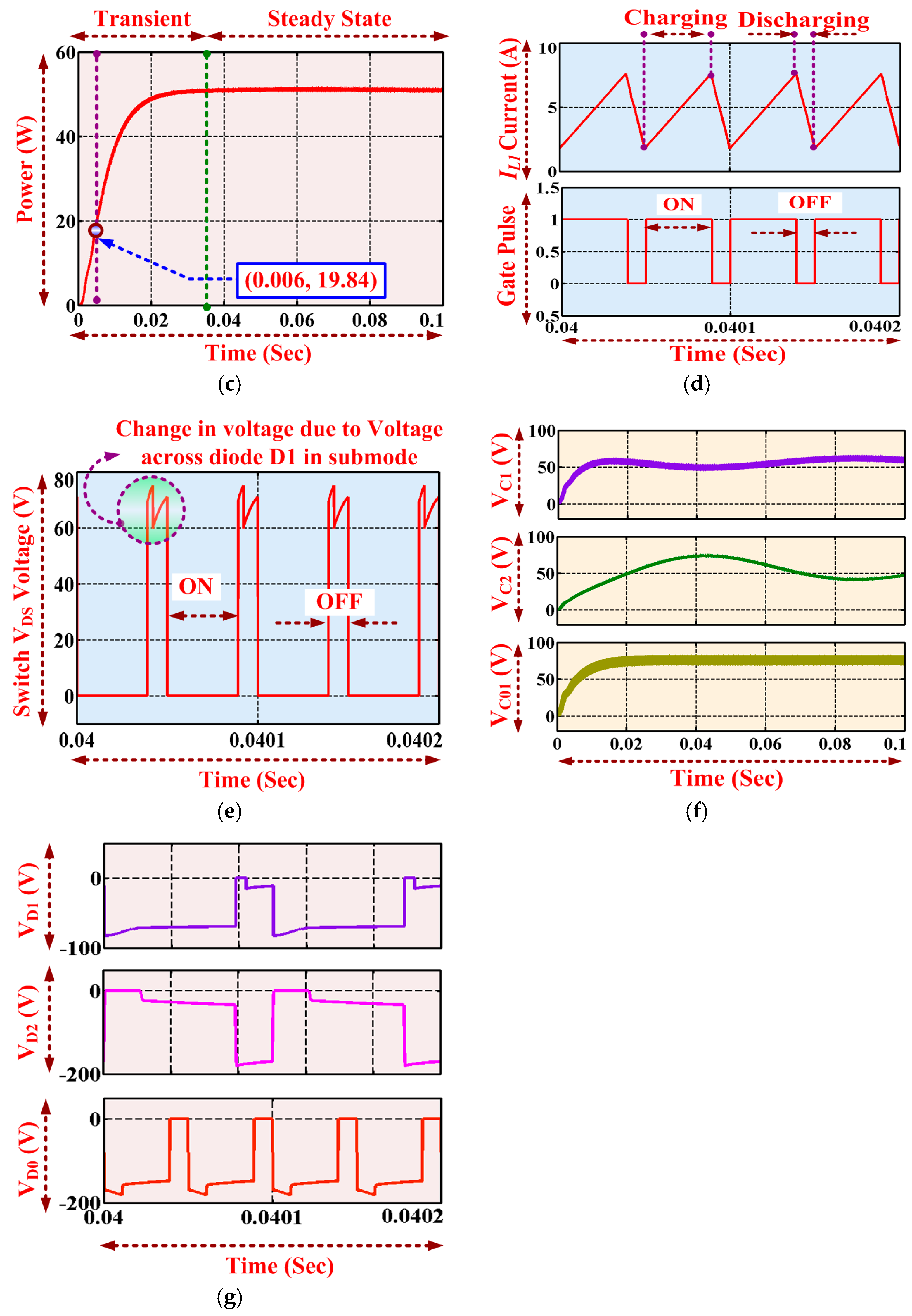
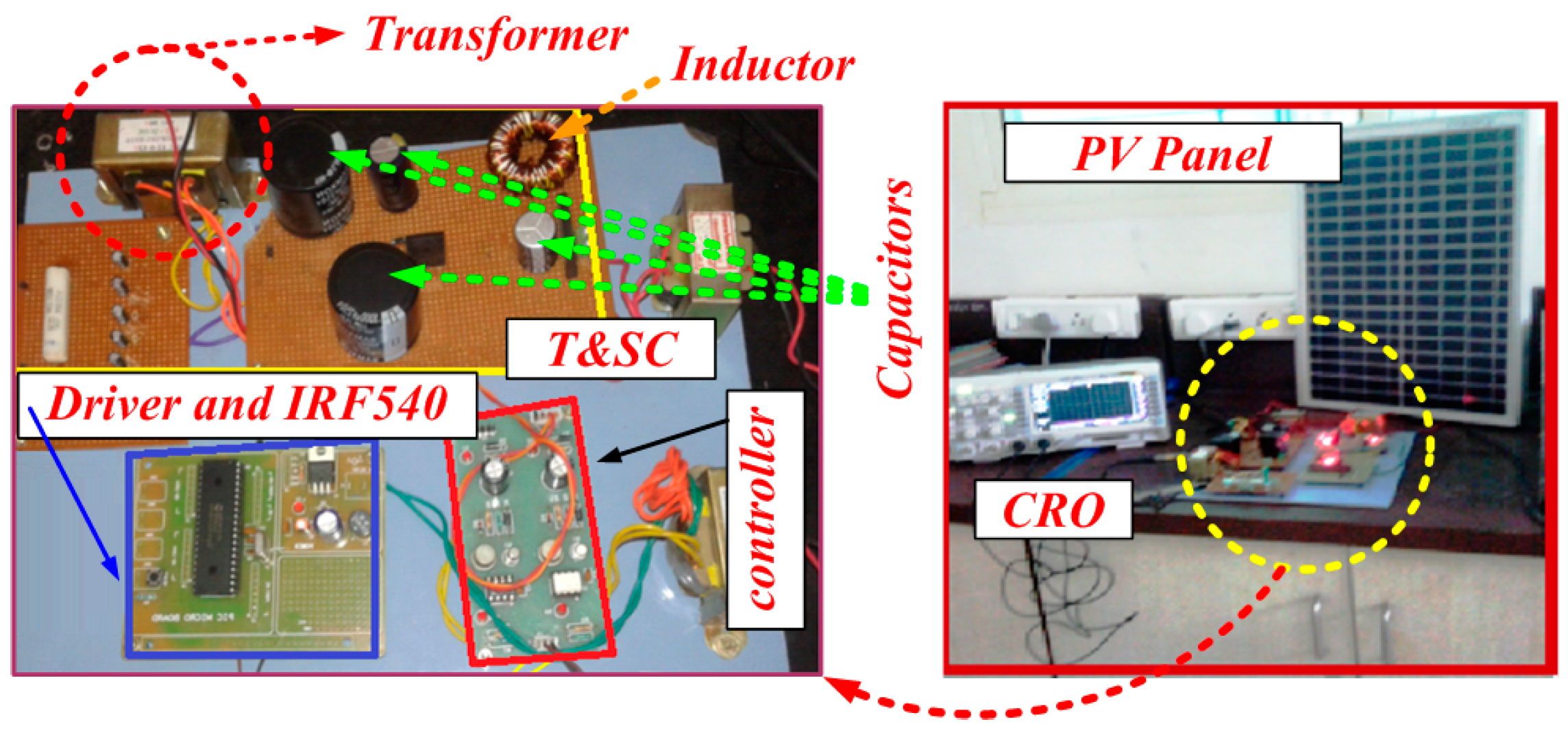
5. Simulation and Experimental Results
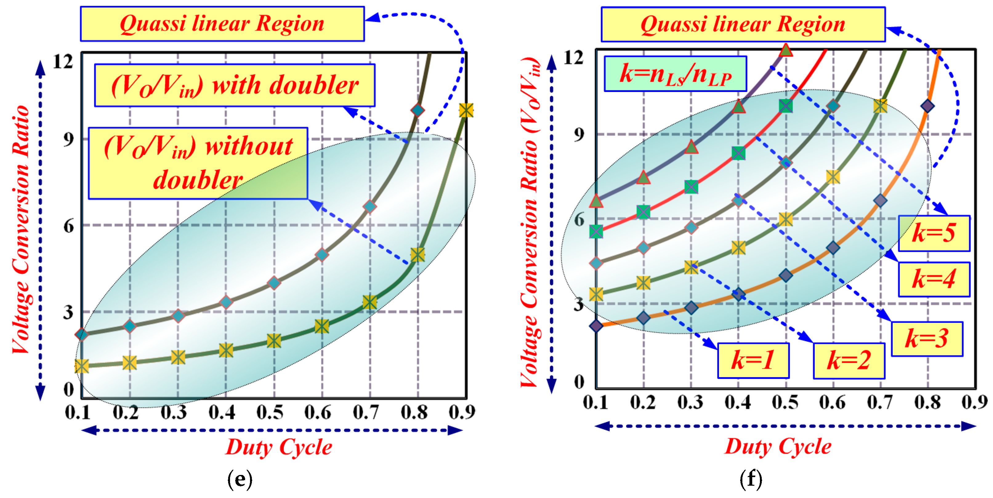
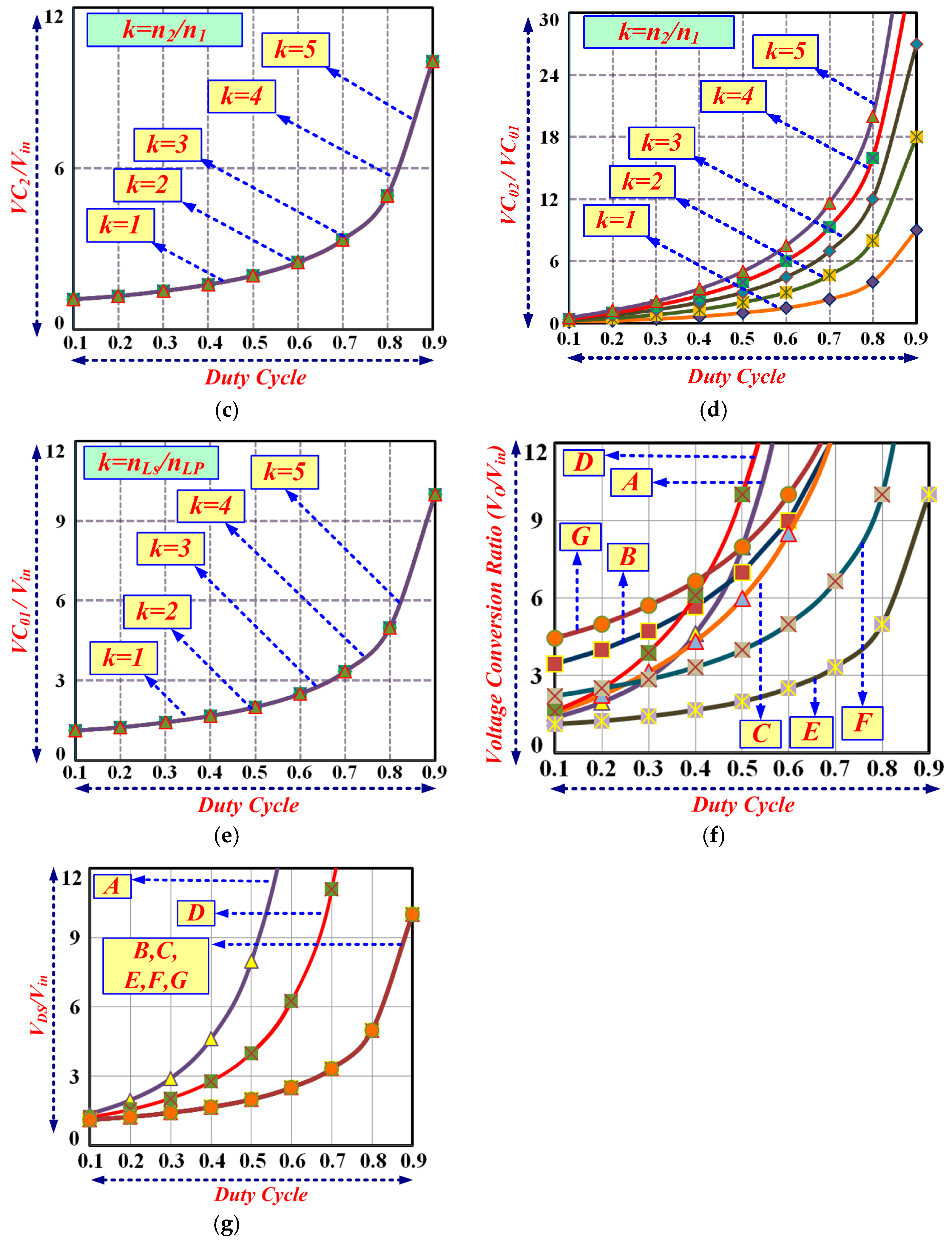
6. Future Extension and Combination of the Proposed T & SC-BC Topology with a Voltage Multiplier
7. Conclusions
Author Contributions
Conflicts of Interest
References
- Hussain, S.; Al-ammari, R.; Iqbal, A.; Jafar, M.; Padmanaban, S. Optimization of Hybrid Renewable Energy System Using Iterative Filter Selection Approach. IET Renew. Power Gener. 2017, 11, 1440–1445. [Google Scholar] [CrossRef]
- Chandramohan, K.; Padmanaban, S.; Kalyanasundaram, R.; Bhaskar, M.S.; Mihet-Popa, L. Grid Synchronization of Seven-phase Wind Electric Generator using d-q PLL. Energies 2017, 10, 926. [Google Scholar] [CrossRef]
- REN21. Renewable 2017: Global Status Report. Available online: http://www.ren21.net/ (accessed on 14 June 2017).
- REN21. Global Futures Report: Scenario Profiles Report. Available online: http://www.ren21.net (accessed on 16 January 2013).
- Coster, E.J.; Myrzik, J.M.A.; Kruimer, B.; Kling, W.L. Integration issues of distributed generation in distribution grids. Proc. IEEE 2011, 99, 28–39. [Google Scholar] [CrossRef]
- Teodorescu, R.; Liserre, M.; Rodriguez, P. Grid Converters for Photovoltaic and Wind Power Systems; Wiley: Hoboken, NJ, USA, 2011. [Google Scholar]
- Padmanaban, S.; Pecht, M. An Isolated/Non-Isolated Novel Multilevel Inverter Configuration for Dual Three-Phase Symmetrical/Asymmetrical Converter. Eng. Sci. Technol. Int. J. 2016, 19, 1763–1770. [Google Scholar] [CrossRef]
- Gunabalan, R.; Sanjeevikumar, P.; Blaabjerg, F.; Olorunfemi, O.; Subbiah, V. Analysis and Implementation of Parallel Connected Two Induction Motor Single Inverter Drive by Direct Vector Control for Industrial Application. IEEE Trans. Power Electron. 2015, 30, 6472–6475. [Google Scholar] [CrossRef]
- Dragonas, F.A.; Nerrati, G.; Sanjeevikumar, P.; Grandi, G. High-Voltage High-Frequency Arbitrary Waveform Multilevel Generator for DBD Plasma Actuators. IEEE Trans. Ind. Appl. 2015, 51, 3334–3342. [Google Scholar] [CrossRef]
- Türkay, B.; Telli, A.Y. Economic analysis of standalone and grid connected hybrid energy systems. Renew. Energy 2011, 36, 1931–1943. [Google Scholar] [CrossRef]
- Energy Information Administration (EIA). International Energy Outlook 2009. United States Department of Energy; 2009. Available online: www.eia.doe.gov (accessed on 27 May 2009).
- International Energy Agency (IEA). World Energy Outlook 2012. Available online: www.worldenergyoutlook.org (accessed on 12 November 2012).
- Das, V.; Padmanaban, S.; Venkitusamy, K.; Selvamuthukumaran, R.; Blaabjerg, F.; Siano, P. Recent Advances and Challenges of Fuel Cell Based Power System Architectures and Control—A Review. Renew. Sustain. Energy 2017, 73, 10–18. [Google Scholar] [CrossRef]
- Vavilapalli, S.; Sanjeevikumar, P.; Umashankar, S.; Mihet-Popa, L. Power Balancing Control for Grid Energy Storage System in PV Applications—Real Time Digital Simulation Implementation. Energies 2017, 10, 928. [Google Scholar] [CrossRef]
- European Photovoltaic Industry Association (EPIA). Global Market Outlook for Photo-Voltaic until 2013; EPIA: Brussels, Belgium, 2009. [Google Scholar]
- Timilsina, G.R.; Kurdgelashvili, L.; Narbel, P.A. Solar energy: Markets, economics and policies. Renew. Sustain. Energy 2012, 16, 449–465. [Google Scholar] [CrossRef]
- Blaabjerg, F.; Yang, Y.; Ma, K.; Wang, X. Power Electronics—The key Technology for renewable energy system Integration. In Proceedings of the 4th International Conference on Renewable Energy Research and Application (ICRERA), Palermo, Italy, 22–25 November 2015. [Google Scholar]
- Joshi, A.S.; Dincer, I.; Reddy, B.V. Performance analysis of photovoltaic systems: A review. Renew. Sustain. Energy 2009, 13, 1884–1897. [Google Scholar] [CrossRef]
- Blaabjerg, F.; Ma, K.; Yang, Y. Power Electronics for Renewable Energy Systems—Status and Trends. In Proceedings of the 8th International Conference on Integrated Power Systems (CIPS), Nuremberg, Germany, 25–27 February 2014. [Google Scholar]
- Liu, C.; Wu, B.; Cheung, R. Advanced Algorithm for Control of Photovoltaic Systems. In Proceedings of the Canadian Solar Buildings Conference, Montreal, QC, Canada, 20–24 August 2004. [Google Scholar]
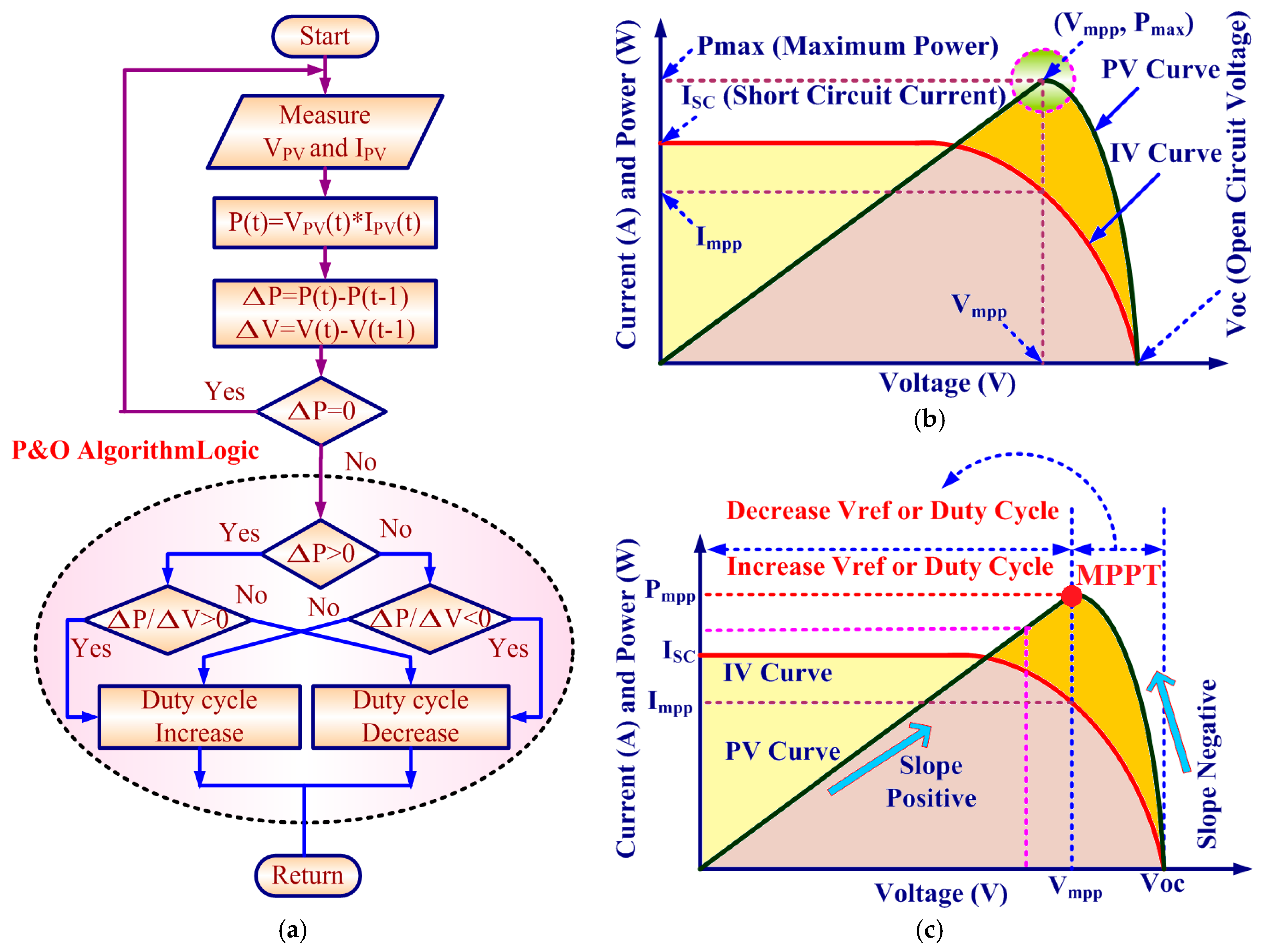
- Gupta, A.; Chauhan, Y.; Pachauri, R. A comparative investigation of maximum power point tracking methods for solar PV system. Sol. Energy 2016, 136, 236–253. [Google Scholar] [CrossRef]
- Sanjeevikumar, P.; Grandi, G.; Wheeler, P.; Blaabjerg, F.; Loncarski, J. A Simple MPPT Algorithm for Novel PV Power Generation system by High Output Voltage DC-DC Boost Converter. In Proceedings of the 24th IEEE International Symposium on Industrial Electronics, Rio de Janeiro, Brazil, 3–5 June 2015; pp. 214–220. [Google Scholar]
- Sanjeevikumar, P.; Blaabjerg, F.; Wheeler, P.; Ojo, J.O.; Ertas, A. High-Voltage DC-DC Converter Topology for PV Energy Utilization—Investigation and Implementation. J. Electr. Power Compon. Syst. 2016, 1–12. [Google Scholar] [CrossRef]
- Mahajan, S.B.; Sanjeevikumar, P.; Blaabjerg, F. A Multistage DC-DC Step-up Self Balanced and Magnetic Component–Free Converter for photovoltaic Application: Hardware Implementation. Energies 2017, 10, 719. [Google Scholar] [CrossRef]
- Tofoli, F.L.; Pereira, D.C.; Paula, W.J. Comparative Study of Maximum Power Point Tracking Techniques for Photovoltaic Systems. Int. J. Photoenergy 2015, 2015, 812582. [Google Scholar] [CrossRef]
- Jain, S.; Ramulu, C.; Padmanaban, S.; Ojo, J.O.; Ertas, A.H. Dual MPPT Algorithm for Dual PV Source Fed Open-End Winding Induction Motor Drive for Pumping Application. Eng. Sci. Technol. Int. J. 2016, 19, 1771–1780. [Google Scholar] [CrossRef]
- Subudhi, B.; Pradhan, R. A comparative study on maximum power point tracking techniques for photovoltaic power systems. IEEE Trans. Sustain. Energy 2013, 4, 89–98. [Google Scholar] [CrossRef]
- Gules, R.; dos Santos, W.M.; dos Reis, F.A.; Romaneli, E.F.R.; Badin, A.A. A Modified Sepic Converter with High Static gain for Renewable Applications. IEEE Trans. Power Electron. 2014, 29, 5860–5871. [Google Scholar] [CrossRef]
- Meneses, D.; Blaabjerg, F.; Garcia, O.; Cobos, J. Review and comparison of step-up transformerless topologies for photovoltaic AC-Module application. IEEE Trans. Power Electron. 2013, 28, 2649–2663. [Google Scholar] [CrossRef]
- Forouzesh, M.; Siwakoti, Y.; Gorji, S.; Blaabjerg, F.; Lehman, B. Step-up DC–DC Converters: A Comprehensive Review of Voltage Boosting Techniques, Topologies, and Applications. IEEE Trans. Power Electron. 2017. [Google Scholar] [CrossRef]
- Tofoli, F.L.; Dênis de Castro, P.; Josias de Paula, W.; de Sousa Oliveira Júnior, D. Survey on non-isolated high-voltage step-up dc–dc topologies based on the boost converter. IET Power Electron. 2015. [Google Scholar] [CrossRef]
- Prudente, M.; Pfitscher, L.; Emmendoerfer, G.; Romaneli, E.; Gules, R. Voltage multiplier cells applied to non-isolated DC–DC converters. IEEE Trans. Power Electron. 2008, 23, 871–887. [Google Scholar] [CrossRef]
- Zhou, D.; Pietkiewicz, A.; Cuk, S. A Three-Switch high-voltage converter. IEEE Trans. Power Electron. 1999, 14, 177–183. [Google Scholar] [CrossRef]
- Henn, G.; Silva, R.; Praca, P.; Barreto, L.; Oliveira, D. Interleaved boost converter with high voltage gain. IEEE Trans. Power Electron. 2010, 25, 2753–2761. [Google Scholar] [CrossRef]
- Wai, R.; Lin, C.; Duan, R.; Chang, Y. High-Efficiency DC-DC converter with high voltage gain and reduced switch stress. IEEE Trans. Ind. Electron. 2007, 54, 1354–1364. [Google Scholar] [CrossRef]
- Wai, R.; Duan, R. High-efficiency power conversion for low power fuel cell generation system. IEEE Trans. Power Electron. 2005, 20, 847–856. [Google Scholar] [CrossRef]
- Li, W.; He, X. A family of interleaved DC–DC converters deduced from a basic cell with winding-cross-coupled inductors (WCCIs) for high step-up or step-down conversions. IEEE Trans. Power Electron. 2008, 23, 1791–1801. [Google Scholar] [CrossRef]
- Young, C.; Chen, M.; Chang, T.; Ko, C.; Jen, K. Cascade Cockcroft–Walton Voltage Multiplier Applied to Transformer-less High Step-up DC–DC Converter. IEEE Trans. Ind. Electron. 2013, 60, 523–537. [Google Scholar] [CrossRef]
- Tomaszuk, A.; krupa, A. High efficiency high step-up DC/DC converters—A review. Bull. Pol. Acad. Sci. Tech. Sci. 2011, 59. [Google Scholar] [CrossRef]
- Chen, S.; Liang, T.; Yang, L.; Chen, J. A Cascaded High Step-up DC–DC Converter with Single Switch for Microsource Applications. IEEE Trans. Power Electron. 2011, 26. [Google Scholar] [CrossRef]
- Mahajan, S.B.; Kulkarni, R.; Sanjeevikumar, P.; Siano, P.; Blaabjerg, F. Hybrid Non-Isolated and Non Inverting Nx Interleaved DC-DC Multilevel Boost Converter for Renewable Energy Applications. In Proceedings of the 16th IEEE International Conference on Environment and Electrical Engineering, Florence, Italy, 7–10 June 2016; pp. 1–6. [Google Scholar]
- Mahajan, S.B.; Kulkarni, R.; Sanjeevikumar, P.; Blaabjerg, F.; Fedák, V.; Cernat, M. Non Isolated and Non-Inverting Cockcroft Walton Multiplier Based Hybrid 2Nx Interleaved Boost Converter for Renewable Energy Applications. In Proceedings of the 17th IEEE Conference on the Power Electronics and Motion Control, Varna, Bulgaria, 25–30 September 2016; pp. 146–151. [Google Scholar]
- Mahajan, S.B.; Sanjeevikumar, P.; Blaabjerg, F.; Norum, L.; Ertas, A. 4Nx Non-Isolated and Non-Inverting Hybrid Interleaved Boost Converter Based on VLSI Cell and Cockroft Walton Voltage Multiplier for Renewable Energy Applications. In Proceedings of the IEEE International Conference on Power Electronics, Drives and Energy Systems, Trivandrum, India, 14–17 December 2016; pp. 1–6. [Google Scholar]
- Mahajan, S.B.; Sanjeevikumar, P.; Ojo, O.; Marco, R.; Kulkarani, R. Non-Isolated and Inverting Nx Multilevel Boost Converter For Photovoltaic DC Link Applications. In Proceedings of the IEEE International Conference on Automatica, XXII Congress of the Chilean Association of Automatic Control, Talca, Chile, 19–21 October 2016; pp. 1–8. [Google Scholar]
- Mahajan, S.B.; Sanjeevikumar, P.; Blaabjerg, F.; Kulkarni, R.; Seshagiri, S.; Hajizadeh, A. Novel LY Converter Topologies for High Gain Transfer Ratio-A New Breed of XY Family. In Proceedings of the 4th IET International Conference on Clean Energy and Technology (IET_CEAT16), Kuala Lumpur, Malaysia, 14–15 November 2016. [Google Scholar]
- Mahajan, S.B.; Sanjeevikumar, P.; Wheeler, P.; Blaabjerg, F.; Rivera, M.; Kulkarni, R. XY Converter Family: A New Breed of Buck Boost Converter for High Step-up Renewable Energy Applications. In Proceedings of the Proceedings of the IEEE International Conference on Automatica, XXII Congress of the Chilean Association of Automatic Control (IEEE-ICA/ACCA’16), Talca, Chile, 19–21 October 2016; pp. 1–8. [Google Scholar]
- Axelrod, B.; Berkovich, Y.; Ioinovici, A. Switched-Capacitor/Switched-Inductor structures for getting transformerless hybrid DC–DC PWM converters. IEEE Trans. Circuits Syst. I Regul. Pap. 2008, 55, 687–696. [Google Scholar] [CrossRef]
- Villalva, M.; Gazoli, J.R.; Filho, E. Comprehensive Approach to Modeling and Simulation of Photovoltaic Arrays. IEEE Trans. Power Electron. 2009, 24, 1198–1208. [Google Scholar] [CrossRef]
- Bendib, B.; Belmili, H.; Krim, F. A survey of the most used MPPT methods: Conventional and advanced algorithms applied for photovoltaic systems. Renew. Sustain. Energy Rev. 2015, 45, 637–648. [Google Scholar] [CrossRef]
- Safari, A.; Mekhilef, S. Simulation and Hardware Implementation of Incremental Conductance MPPT with Direct Control Method Using Cuk Converter. IEEE Trans. Ind. Electron. 2011, 58. [Google Scholar] [CrossRef]
- Saad Saoud, M.; Abbassi, H.; Kermiche, S.; Nada, D. Improved incremental conductance method for maximum power point tracking using cuk converter. Mediterr. J. Model. Simul. 2014, 57–65. Available online: http://www.webreview.dz/IMG/pdf/mjms_01_2014_057-065.pdf (accessed on 1 January 2014).
- Hartmann, L.V.; Vitorino, M.A.; de Rossiter Correa, M.B.; Lima, A.M.N. Combining model-based and heuristic techniques for fast tracking the maximum power point of photovoltaic systems. IEEE Trans. Power Electron. 2013, 28, 2875–2885. [Google Scholar] [CrossRef]
- Esram, T.; Chapman, P. Comparison of Photovoltaic Array Maximum Power Point Tracking Techniques. IEEE Trans. Energy Convers. 2007, 22. [Google Scholar] [CrossRef]


| DC-DC Converter | Voltage Conversion Ratio (Vo/Vin) | Number of Switches | Number of Inductors | Number of Capacitors | Number of Diodes |
|---|---|---|---|---|---|
| Single switch n-stage CBC [38] | 1 | n | n | 2n − 1 | |
| Single switch boost converter with voltage multiplier [38] | 1 | 2 | 2n + 1 | 2n | |
| Coupled inductor based step-up converter [39] | 1 | 3 (2 Inductor are Coupled) | 3 | 3 | |
| Quadratic Boost Converter (QBC) with coupled inductor [40] | 1 | 3 (2 Inductor are Coupled) | 3 | 4 | |
| Boost converter with voltage doubler (Figure 5a) | 1 | 1 | 3 | 3 | |
| Proposed converter | 1 | 1 Inductor with 1 transformer | 4 | 3 |
| DC-DC Converter | Cost of Converter |
|---|---|
| Single switch n-stage CBC [38] | CS + [n × CL] + [n × CC] + [(2n − 1) × CD] |
| Single switch boost converter with voltage multiplier [38] | CS + [2 × CL] + [(2n + 1) × CC] + [(2n) × CD] |
| Coupled inductor based step-up converter [39] | CS + [(1 × CcL) + (1 × CL)] + [3 × CC] + [3 × CD] |
| QBC with coupled inductor [40] | CS + [(1 × CcL) + (1 × CL)] + [3 × CC] + [4 × CD] |
| Boost converter with voltage doubler (Figure 5a) | Cs + CL + [3 × CC] + [3 × CD] |
| Proposed T & SC-BC | CS + [(1 × CcL) + (1 × CT)] + [4 × CC] + [3 × CD] |
| DC-DC Converter | Switch Drain to Source Voltage (VDS) | Efficiency | Applications | Output Ripple |
|---|---|---|---|---|
| Single switch n-stage CBC [38] (Figure 2a) | moderate (85–90%) | low/medium power | high | |
| Single switch boost converter with voltage multiplier [38], (Figure 2b) | moderate (85–90%) | low/medium power | high | |
| Coupled inductor based step-up converter [39], (Figure 2c) | high (90–95%) | medium/high power | low | |
| Quadratic Boost Converter (QBC) with coupled inductor [40], (Figure 2d) | high (90–95%) | medium/high power | low | |
| Conventional boost converter with voltage doubler (Figure 5a) | high (90–95%) | low/medium power | high | |
| Proposed converter (Figure 5b) | high (90–95%) | medium/high power | low |
| Parameter | Value |
|---|---|
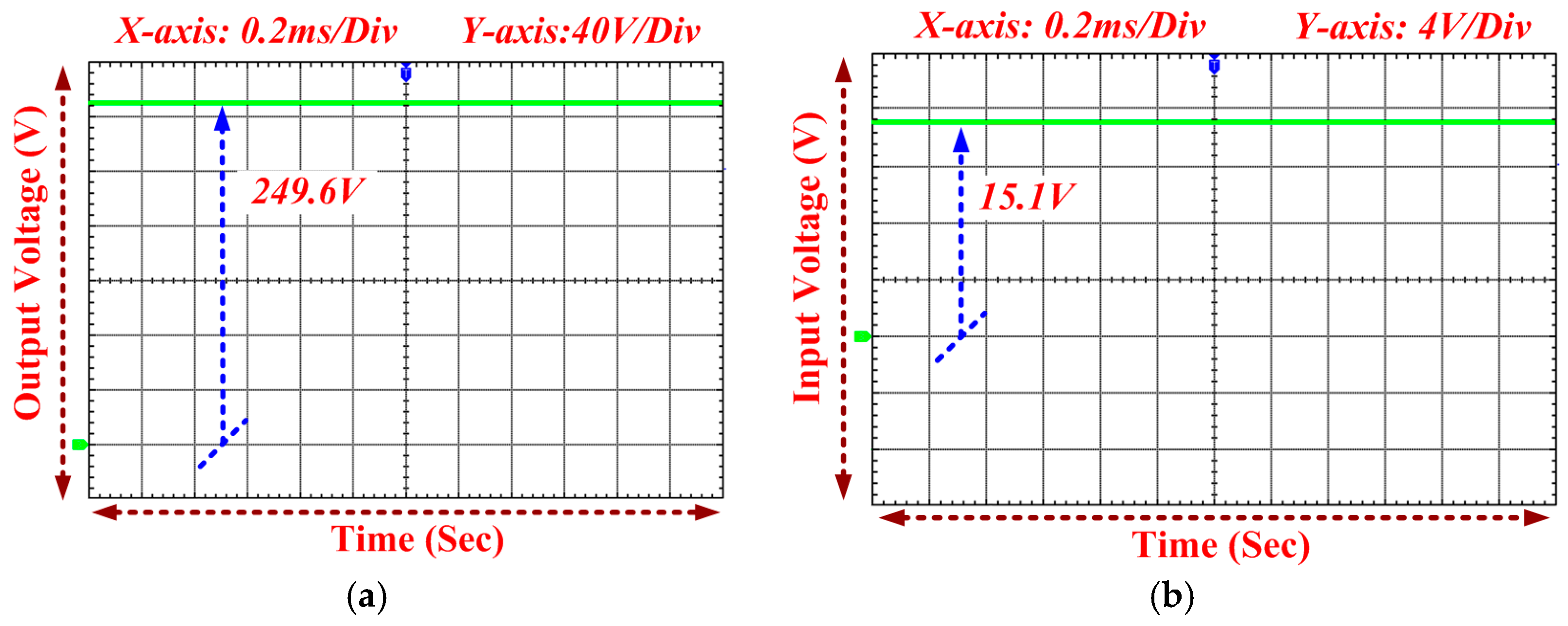
| Input voltage (Vin), Output voltage (Vo) | 15 V, 250 V |
| Input current (Iin), Output current (I o) | 3.34 A, 0.2 A |
| Power (P) | 50 W |
| Duty cycle (D) | 0.784 |
| Switching frequency (fs) | 20 kHz |
| Switch Drain to Source voltage (VDS) | 70 V (Minimum Voltage) |
| Inductor (L1) | 117.6 µH |
| Transformer windings | LP = 117.6 µH, LS = 794.97 µHTurns ratio, k = 2.6 |
| Capacitors (C1, C2) | 2.5 µF, 250 V |
| Capacitor C0 and C01 | 100 µF, 400 V |
| Parameter | Value |
|---|---|
| PV Panel | 3 PV Panels (each of 18 V) |
| Input Voltage (Vin), Output Voltage (Vo) | 15 V, 250 V |
| Input Current (Iin), Output Current (Io) | 3.34 A, 0.2 A |
| Power (P) | 50 W |
| Duty Cycle (D) | 0.784 |
| Switching frequency (fs) | 20 kHz |
| Switch Drain to Source Voltage (VDS) | 70 V (Minimum Voltage) |
| Inductor (L1) | 120 µH |
| Transformer Windings | LP = 120 µH, LS = 800 µH Turns ratio = 2.6 |
| Capacitors (C1 and C2) | 3.3 µF, 250 V |
| Capacitor C0 and C01 | 100 µF, 400 V |
| Diode (D1, D2, D0) | MUR 860 |
| Control Switch | IRF 540 |
© 2018 by the authors. Licensee MDPI, Basel, Switzerland. This article is an open access article distributed under the terms and conditions of the Creative Commons Attribution (CC BY) license (http://creativecommons.org/licenses/by/4.0/).
Share and Cite
Padmanaban, S.; Bhaskar, M.S.; Maroti, P.K.; Blaabjerg, F.; Fedák, V. An Original Transformer and Switched-Capacitor (T & SC)-Based Extension for DC-DC Boost Converter for High-Voltage/Low-Current Renewable Energy Applications: Hardware Implementation of a New T & SC Boost Converter. Energies 2018, 11, 783. https://doi.org/10.3390/en11040783
Padmanaban S, Bhaskar MS, Maroti PK, Blaabjerg F, Fedák V. An Original Transformer and Switched-Capacitor (T & SC)-Based Extension for DC-DC Boost Converter for High-Voltage/Low-Current Renewable Energy Applications: Hardware Implementation of a New T & SC Boost Converter. Energies. 2018; 11(4):783. https://doi.org/10.3390/en11040783
Chicago/Turabian StylePadmanaban, Sanjeevikumar, Mahajan Sagar Bhaskar, Pandav Kiran Maroti, Frede Blaabjerg, and Viliam Fedák. 2018. "An Original Transformer and Switched-Capacitor (T & SC)-Based Extension for DC-DC Boost Converter for High-Voltage/Low-Current Renewable Energy Applications: Hardware Implementation of a New T & SC Boost Converter" Energies 11, no. 4: 783. https://doi.org/10.3390/en11040783
APA StylePadmanaban, S., Bhaskar, M. S., Maroti, P. K., Blaabjerg, F., & Fedák, V. (2018). An Original Transformer and Switched-Capacitor (T & SC)-Based Extension for DC-DC Boost Converter for High-Voltage/Low-Current Renewable Energy Applications: Hardware Implementation of a New T & SC Boost Converter. Energies, 11(4), 783. https://doi.org/10.3390/en11040783