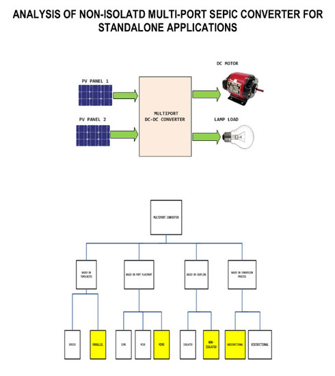
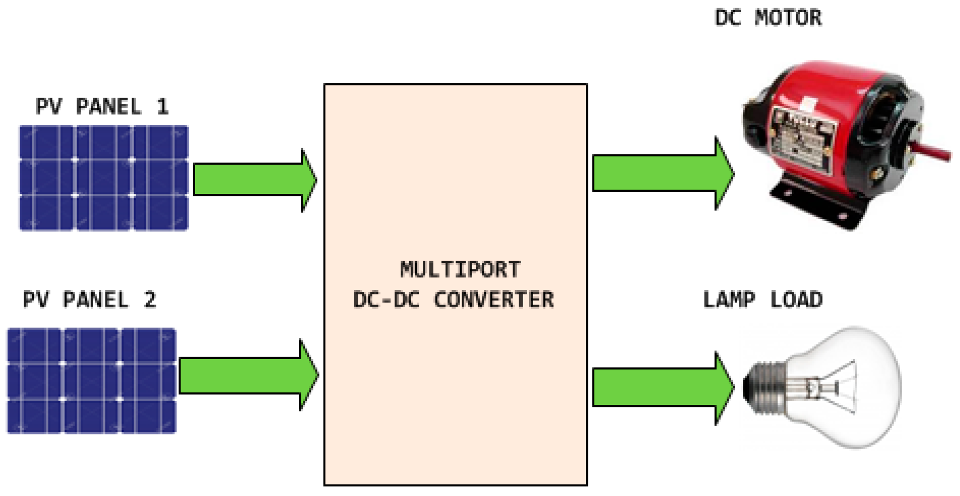
Figure 1.
Conventional multi-input converter.
Figure 1.
Conventional multi-input converter.
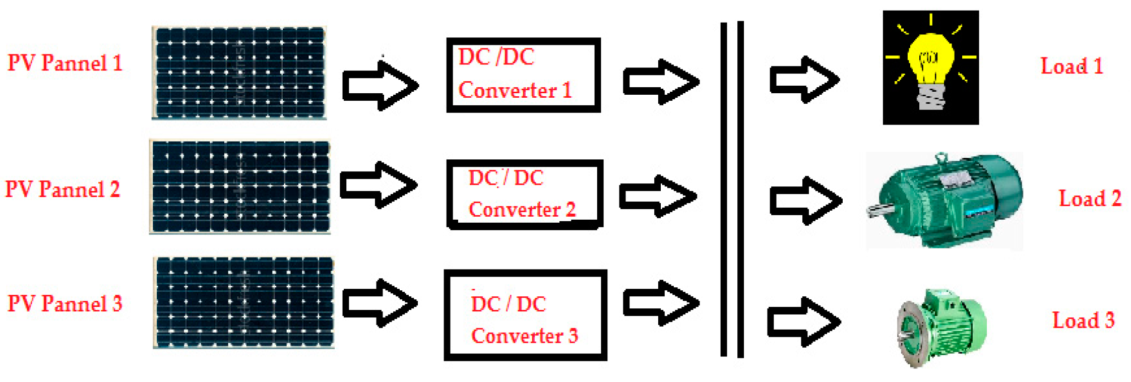
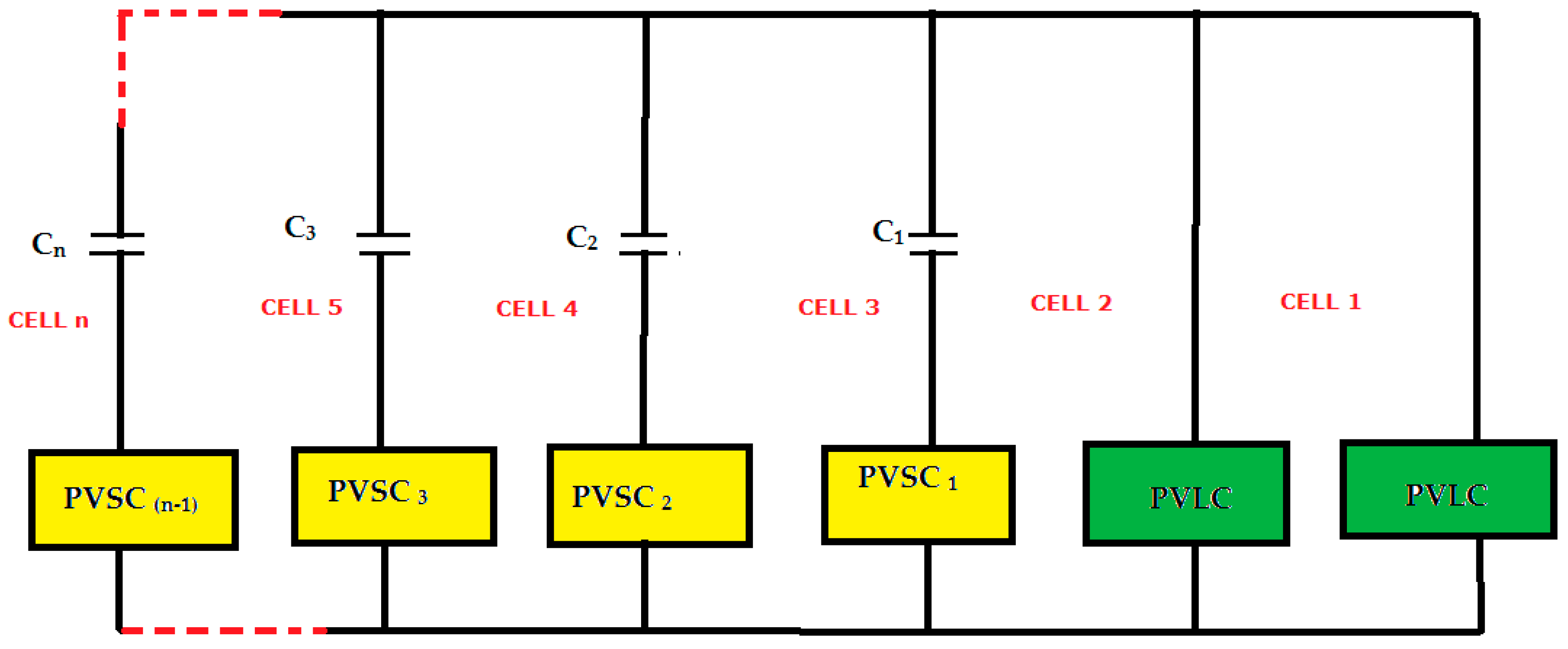
Figure 2.
Multiport structure for four ports.
Figure 2.
Multiport structure for four ports.
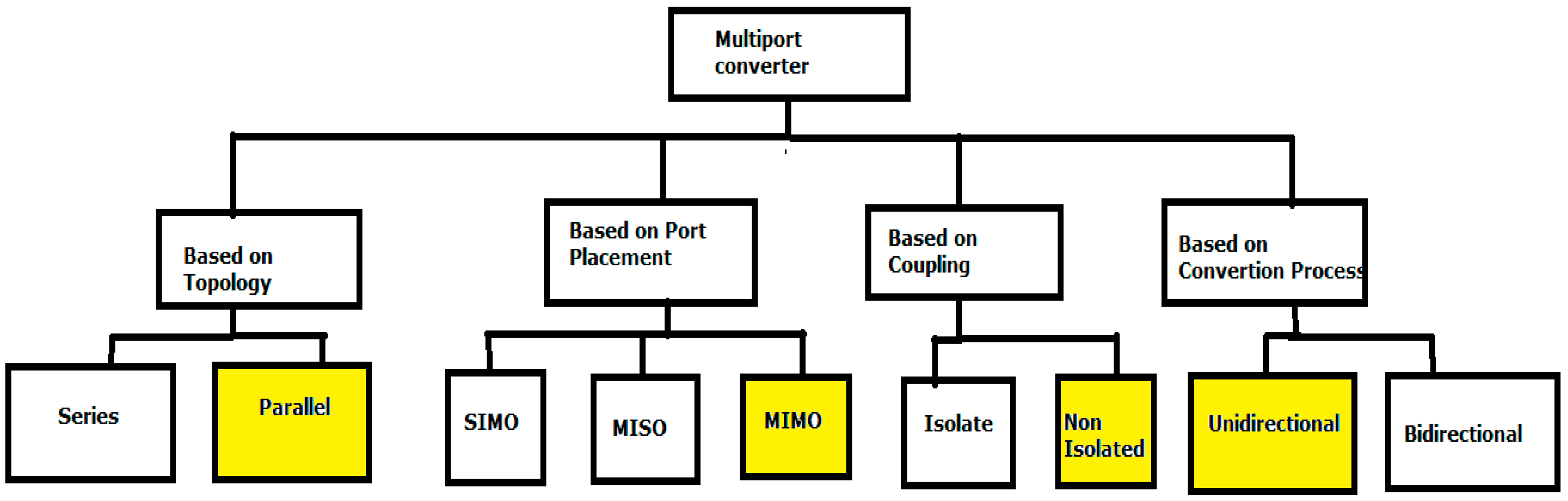
Figure 3.
Classificationof Multiport Converter.
Figure 3.
Classificationof Multiport Converter.
Figure 4.
Circuit diagram of a basic SEPIC converter.
Figure 4.
Circuit diagram of a basic SEPIC converter.
Figure 5.
Three port unidirectional SEPIC converter.
Figure 5.
Three port unidirectional SEPIC converter.
Figure 6.
Generalized diagram for SEPIC converter.
Figure 6.
Generalized diagram for SEPIC converter.
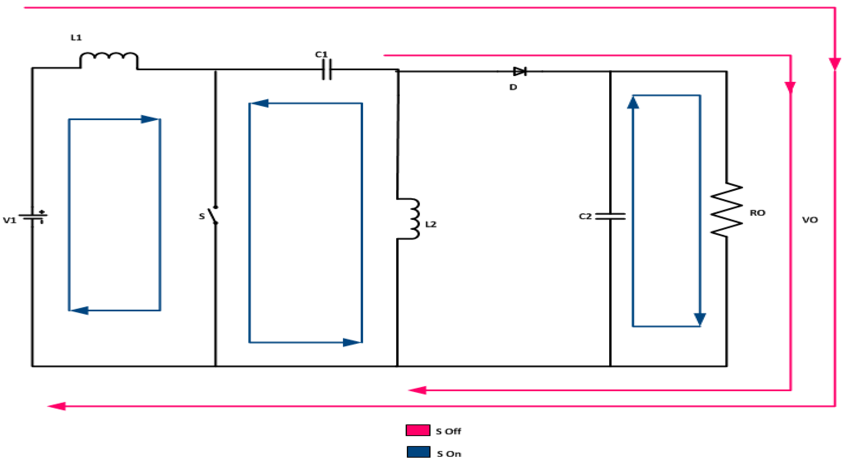
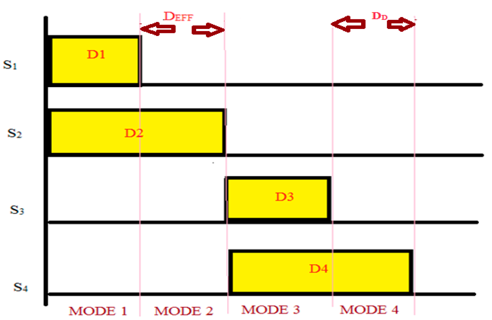
Figure 7.
Modes of operation of the topology.
Figure 7.
Modes of operation of the topology.
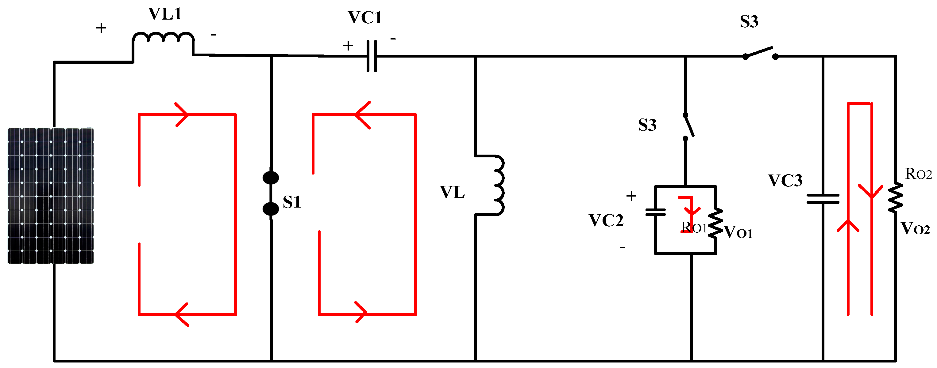
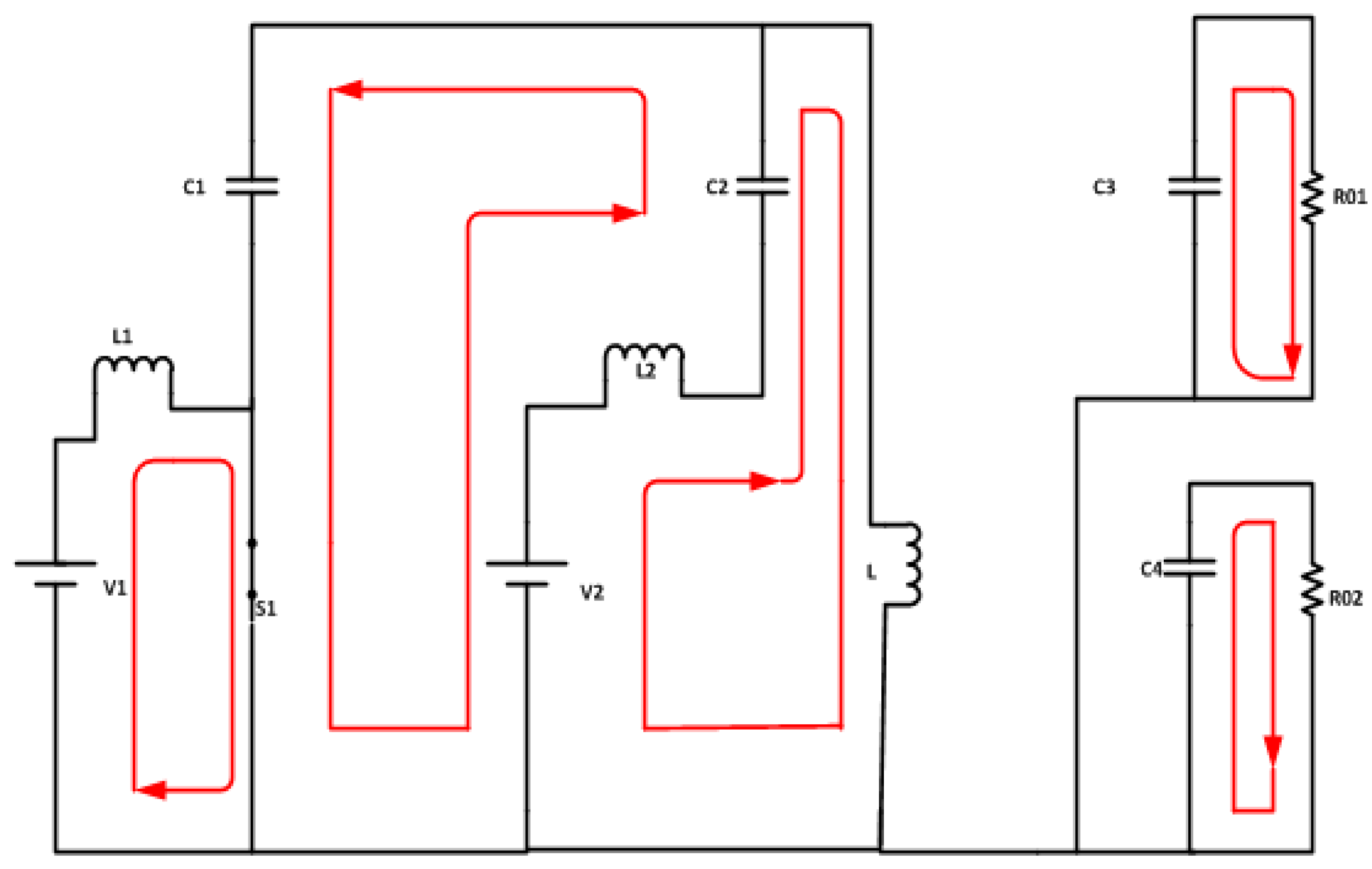
Figure 8.
Mode-1 operation of SIMO SEPIC Converter.
Figure 8.
Mode-1 operation of SIMO SEPIC Converter.
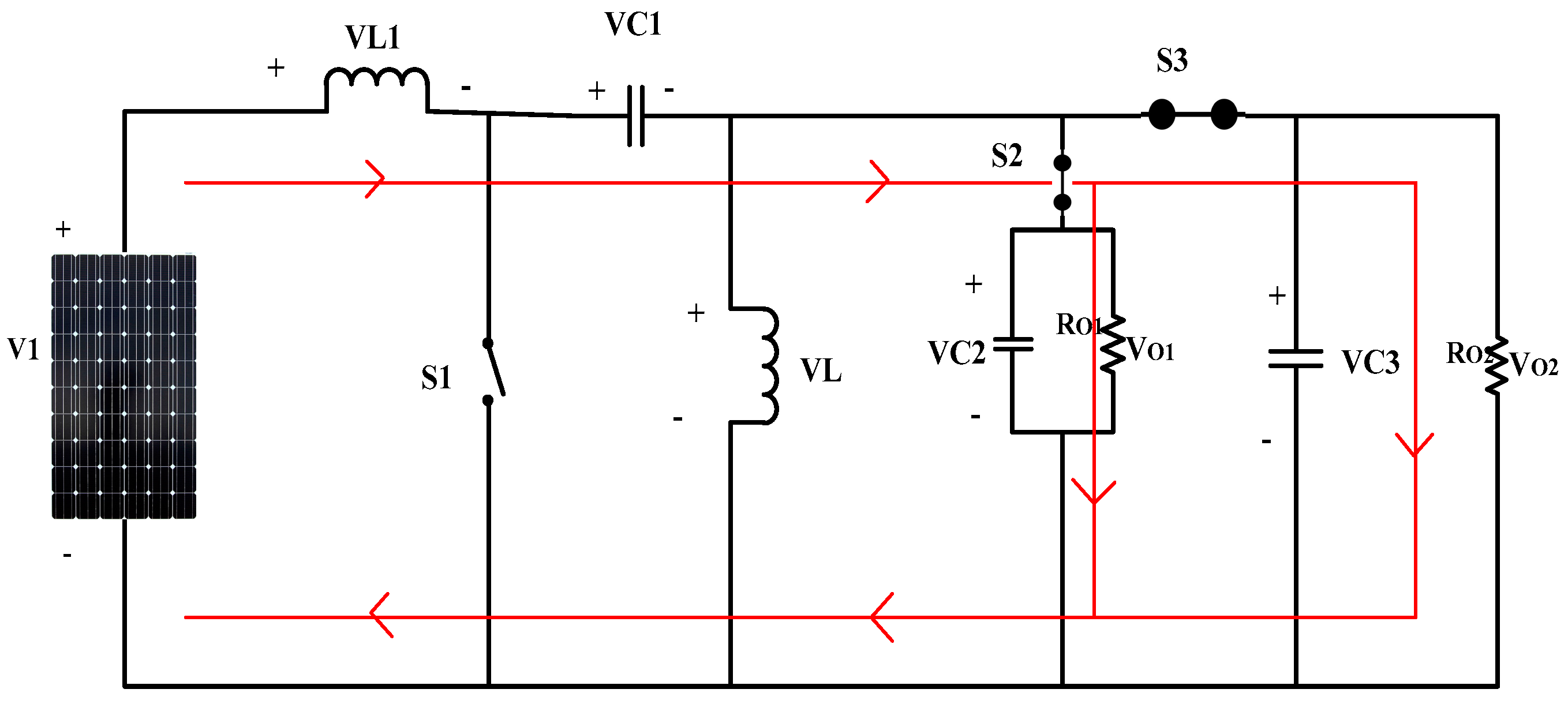
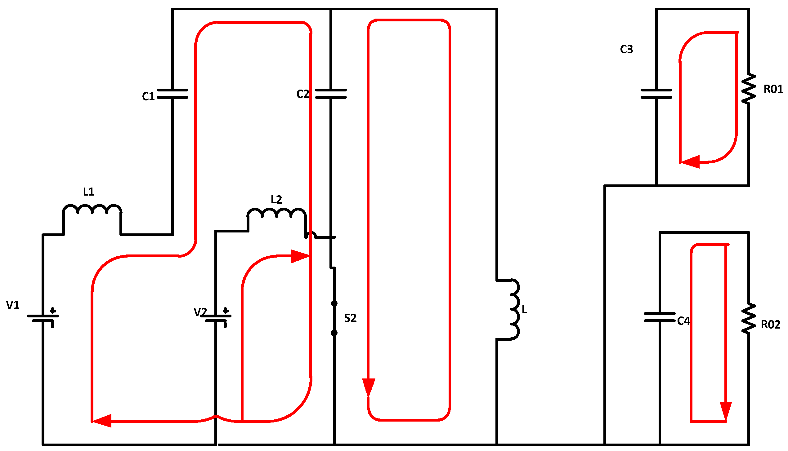
Figure 9.
Mode-2 operation of SIMO SEPIC Converter.
Figure 9.
Mode-2 operation of SIMO SEPIC Converter.
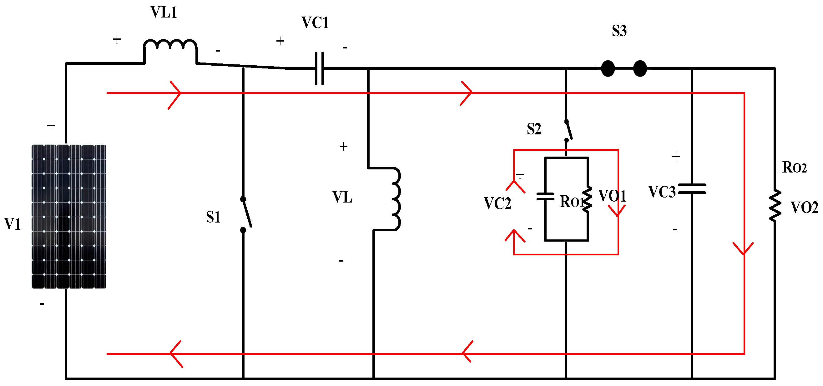
Figure 10.
Mode-3 operation of the SIMO SEPIC.
Figure 10.
Mode-3 operation of the SIMO SEPIC.
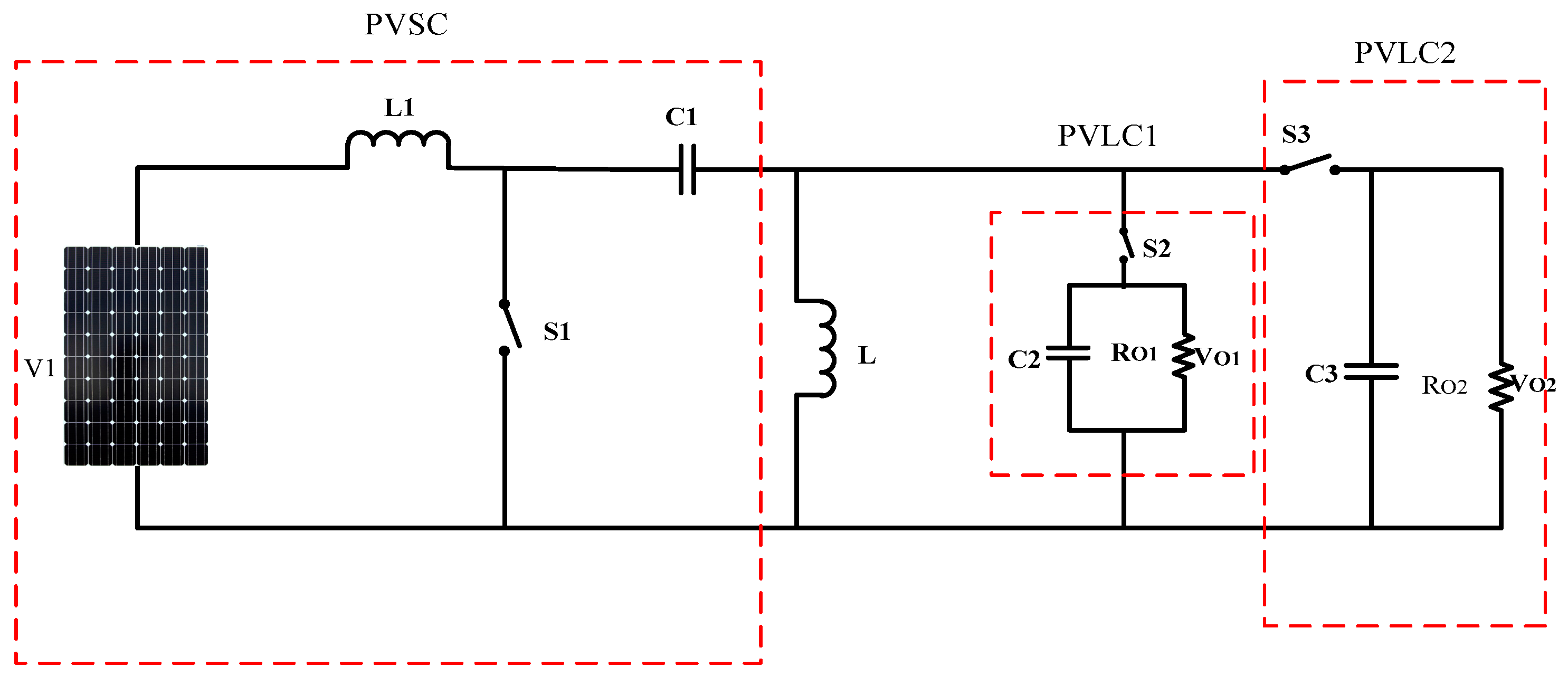
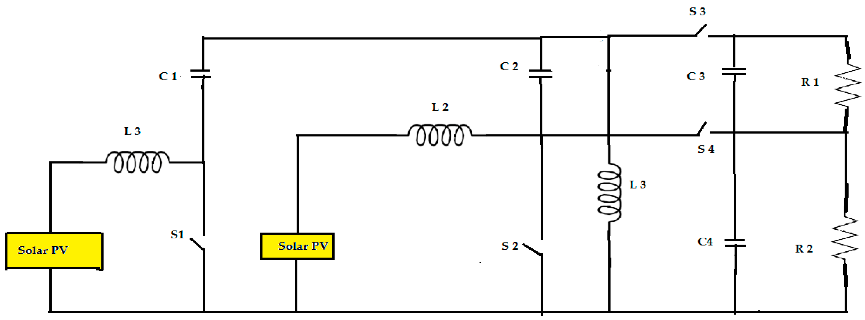
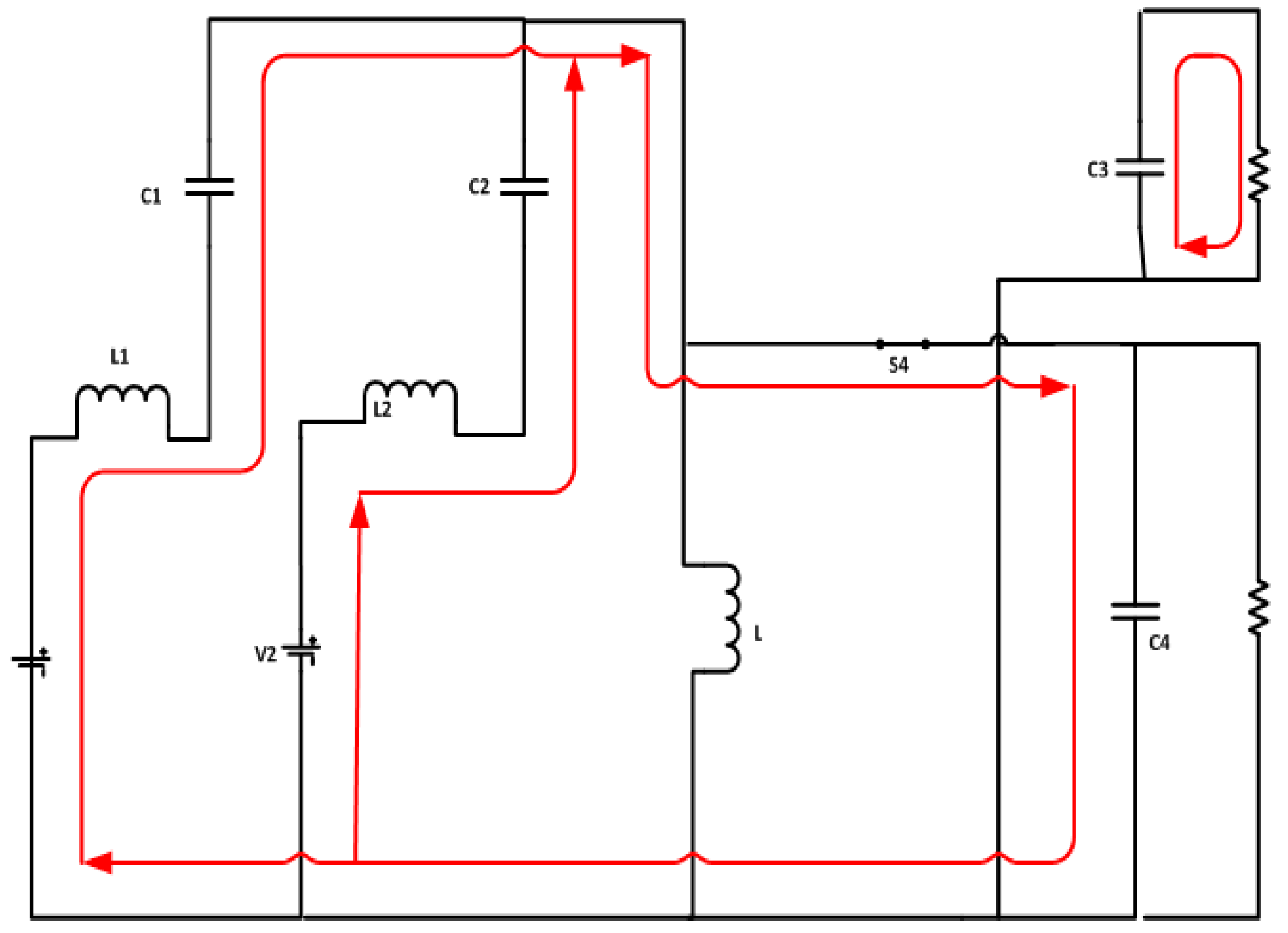
Figure 11.
Four Port SEPIC/SEPIC Converters.
Figure 11.
Four Port SEPIC/SEPIC Converters.
Figure 12.
Modes of operation of MIMO.
Figure 12.
Modes of operation of MIMO.
Figure 13.
Mode-A of the proposed circuit.
Figure 13.
Mode-A of the proposed circuit.
Figure 14.
Mode-B of the proposed circuit.
Figure 14.
Mode-B of the proposed circuit.
Figure 15.
Mode-C of the proposed circuit.
Figure 15.
Mode-C of the proposed circuit.
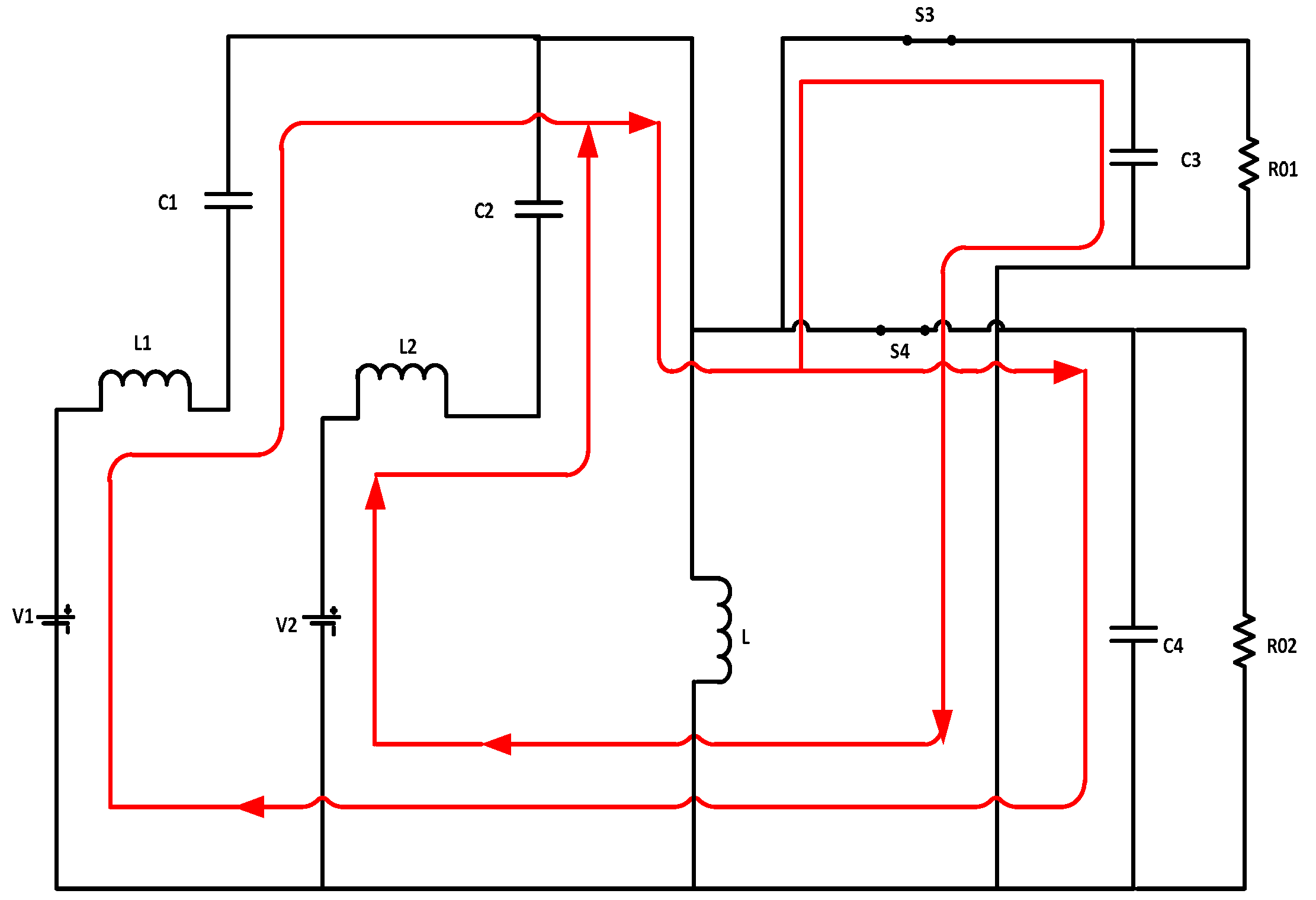
Figure 16.
Mode-D of the proposed circuit.
Figure 16.
Mode-D of the proposed circuit.
Figure 17.
Simulink model for a three port unidirectional SEPIC.
Figure 17.
Simulink model for a three port unidirectional SEPIC.
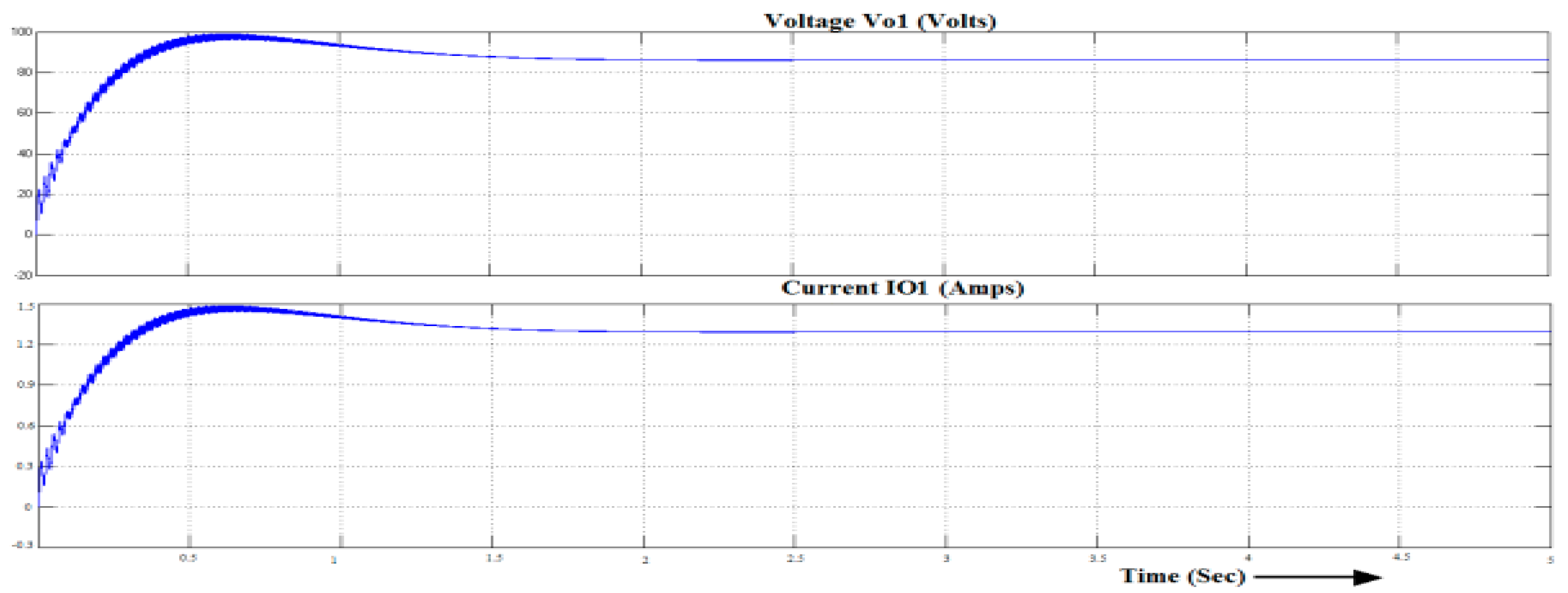
Figure 18.
Output voltage and current waveforms of a SIMO SEPIC.
Figure 18.
Output voltage and current waveforms of a SIMO SEPIC.
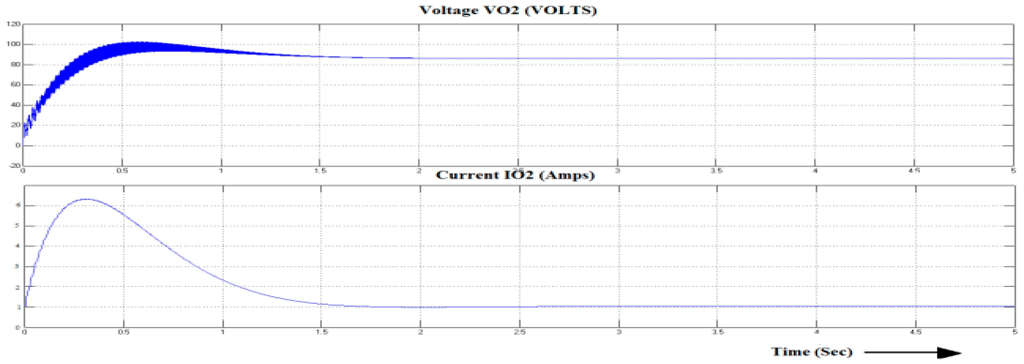
Figure 19.
Output voltage and current waveforms of a SIMO SEPIC.
Figure 19.
Output voltage and current waveforms of a SIMO SEPIC.
Figure 20.
Waveforms of voltage and current of components in PVSC, PVlC2 and PVLC2, respectively.
Figure 20.
Waveforms of voltage and current of components in PVSC, PVlC2 and PVLC2, respectively.
Figure 21.
Waveform of speed and torque of motor.
Figure 21.
Waveform of speed and torque of motor.
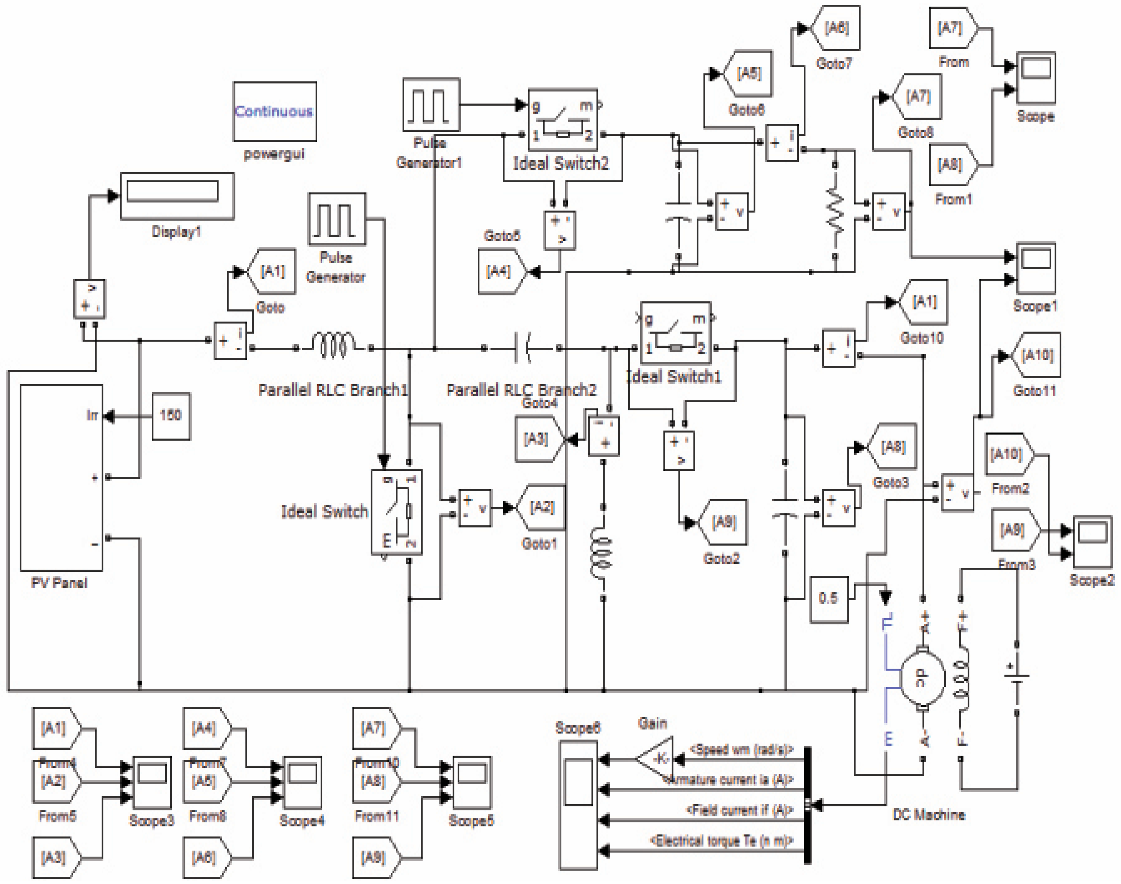
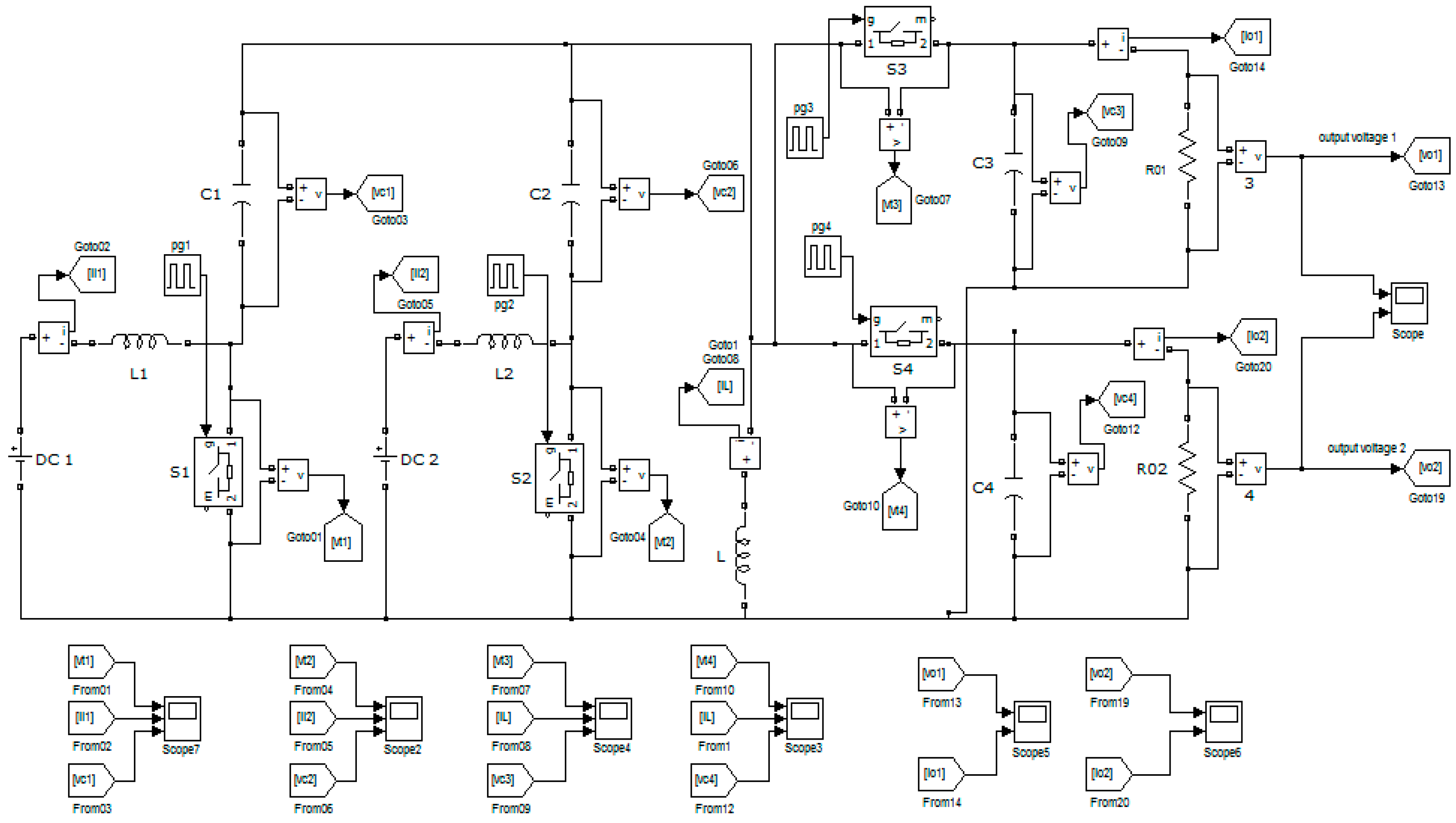
Figure 22.
Simulink Model for a Four Port SEPIC.
Figure 22.
Simulink Model for a Four Port SEPIC.
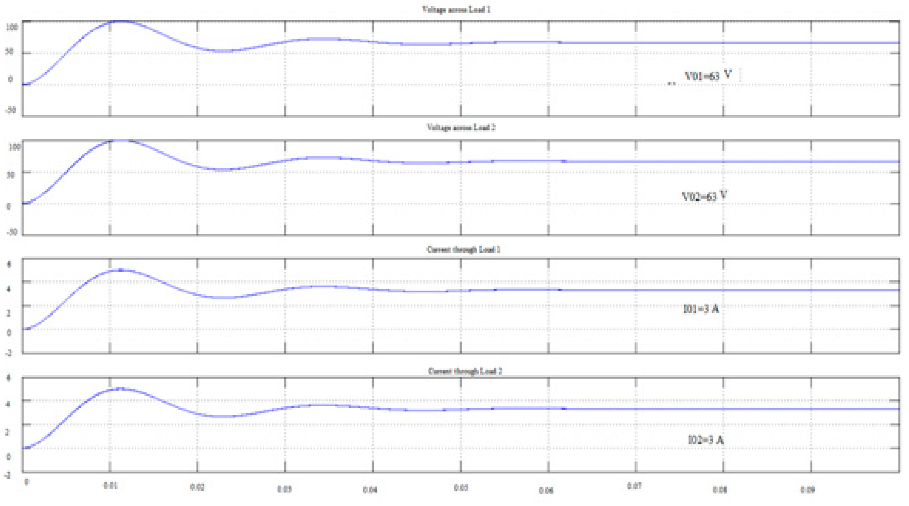
Figure 23.
Output Voltage and Current Waveforms of the Proposed Topology.
Figure 23.
Output Voltage and Current Waveforms of the Proposed Topology.
Figure 24.
Waveforms of voltage and currents across the components of PVSC2.
Figure 24.
Waveforms of voltage and currents across the components of PVSC2.
Figure 25.
Waveforms of voltage and currents across the components of PVLC1.
Figure 25.
Waveforms of voltage and currents across the components of PVLC1.
Figure 26.
Waveforms of voltage and currents across the components of PVLC2.
Figure 26.
Waveforms of voltage and currents across the components of PVLC2.
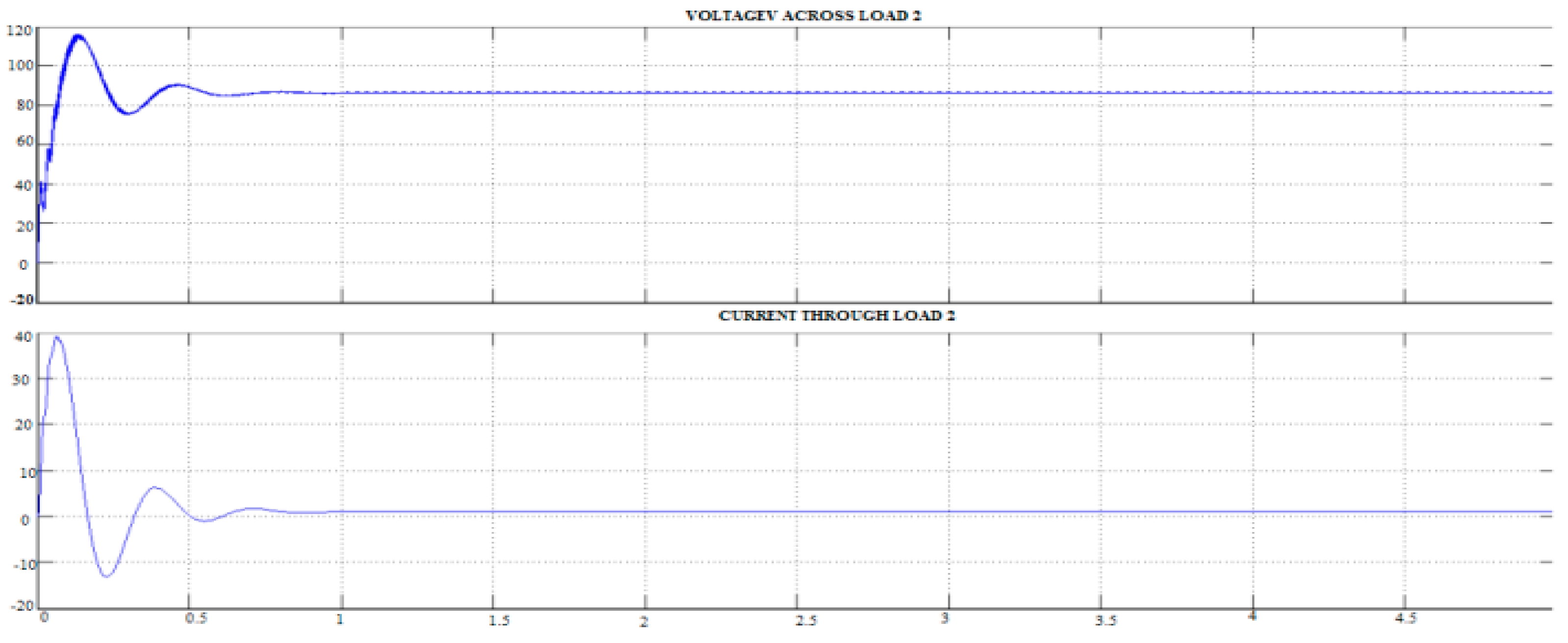
Figure 27.
Waveforms for Load 1.
Figure 27.
Waveforms for Load 1.
Figure 28.
Speed-torque characteristics.
Figure 28.
Speed-torque characteristics.
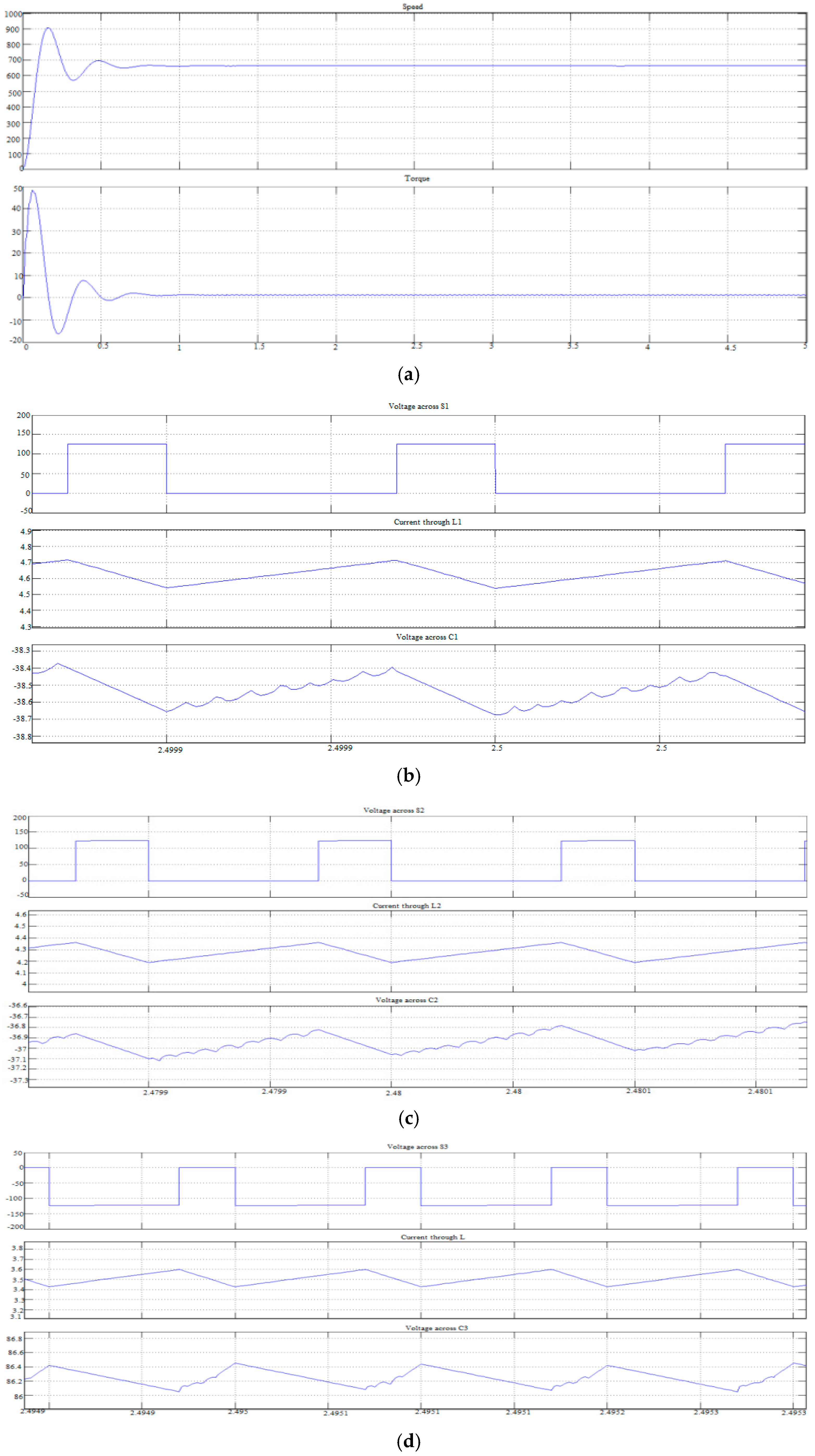
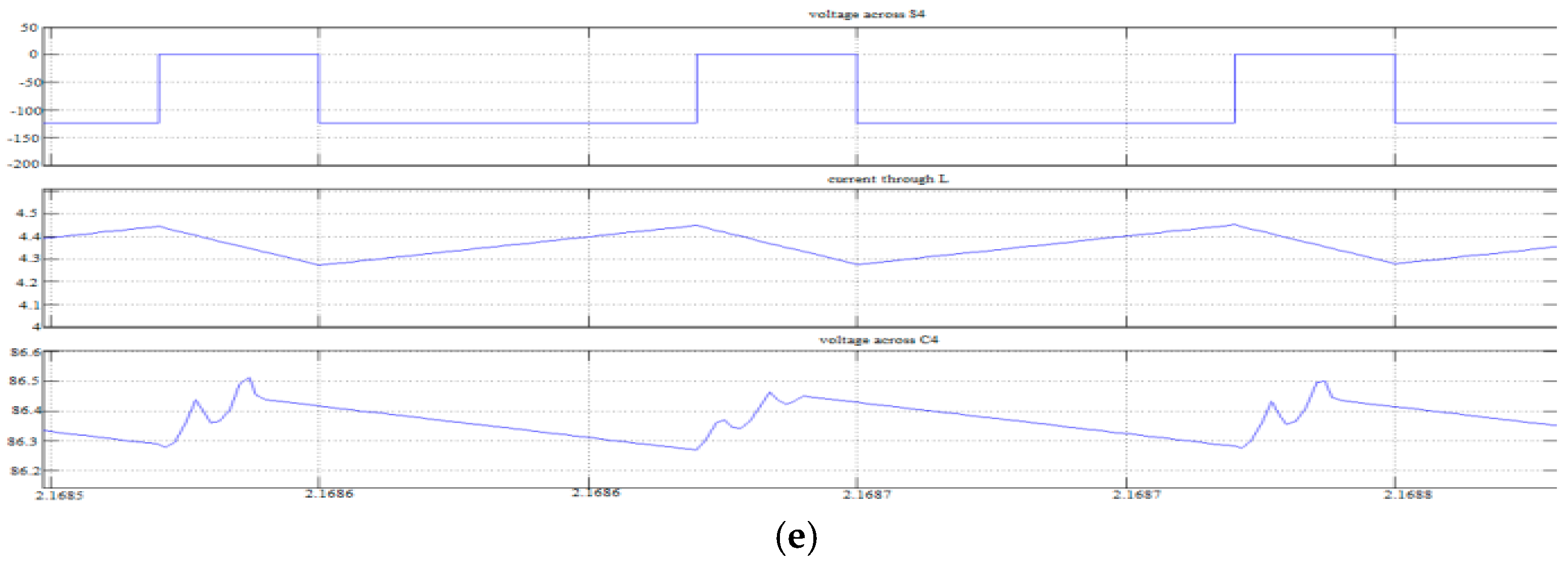
Figure 29.
(a) Waveforms for PVSC1; (b) Waveforms for PVSC2; (c) Waveforms for PVLC1; (d) Waveforms for PVLC2; and (e) Waveforms of voltage and currents across the components of PVSC1, PVSC2, PVLC1 and PVLC2.
Figure 29.
(a) Waveforms for PVSC1; (b) Waveforms for PVSC2; (c) Waveforms for PVLC1; (d) Waveforms for PVLC2; and (e) Waveforms of voltage and currents across the components of PVSC1, PVSC2, PVLC1 and PVLC2.
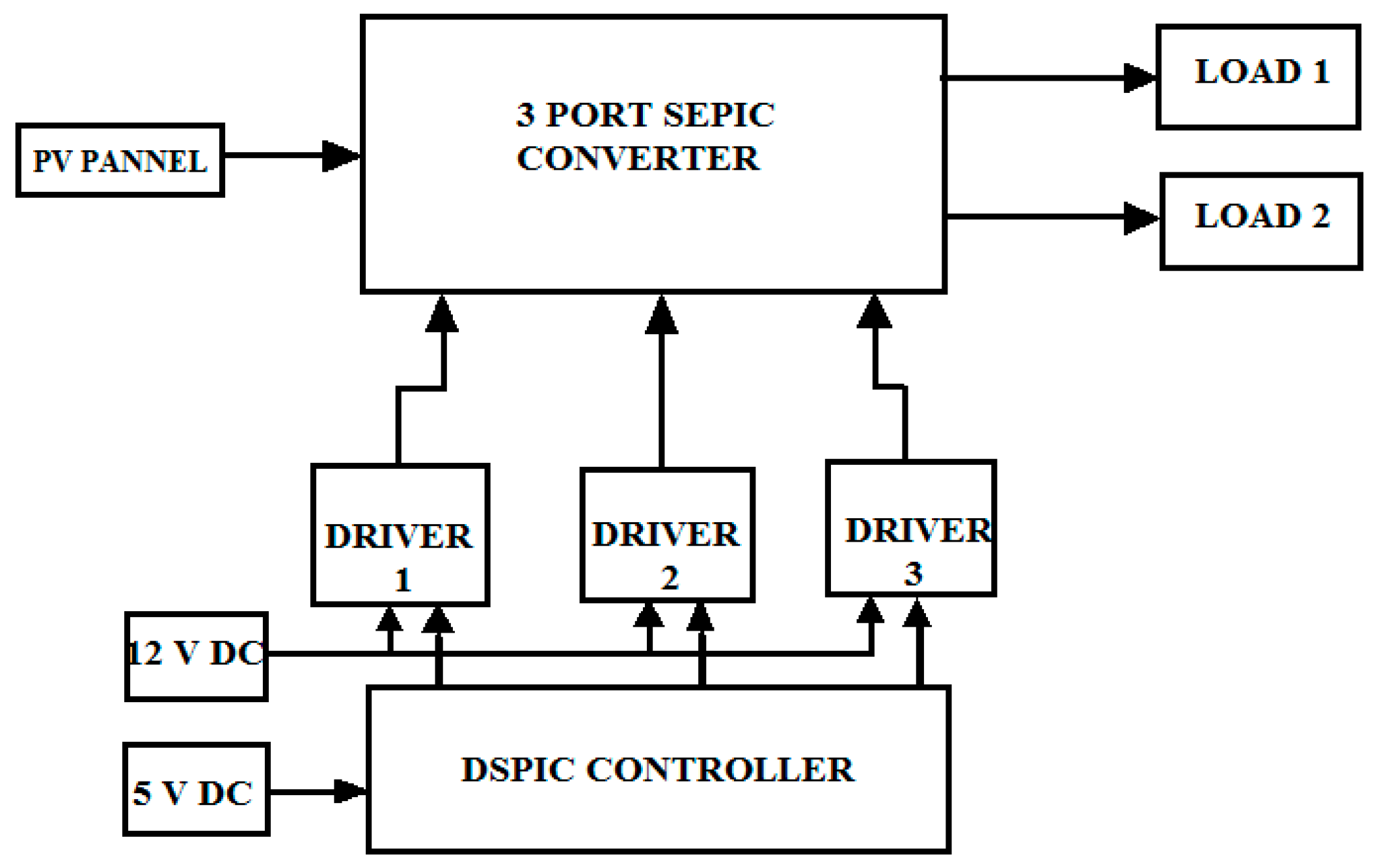
Figure 30.
Block diagram of the hardware setup.
Figure 30.
Block diagram of the hardware setup.
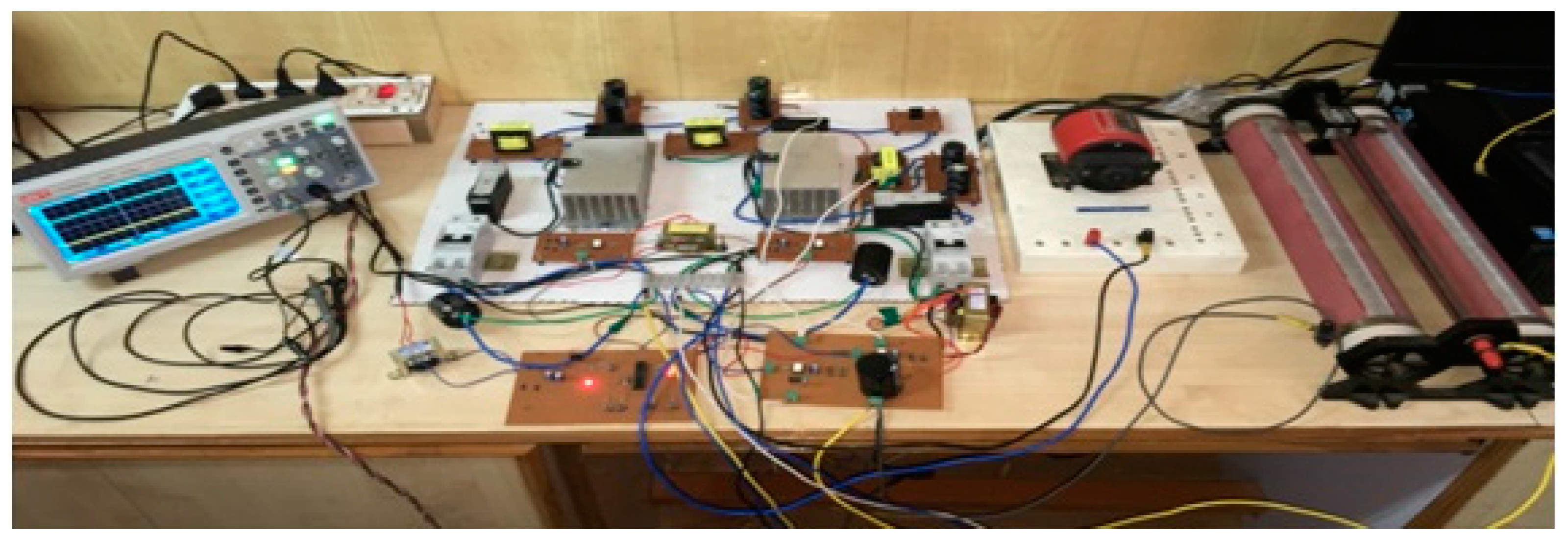
Figure 31.
The complete circuit of the three port SIMO structure.
Figure 31.
The complete circuit of the three port SIMO structure.
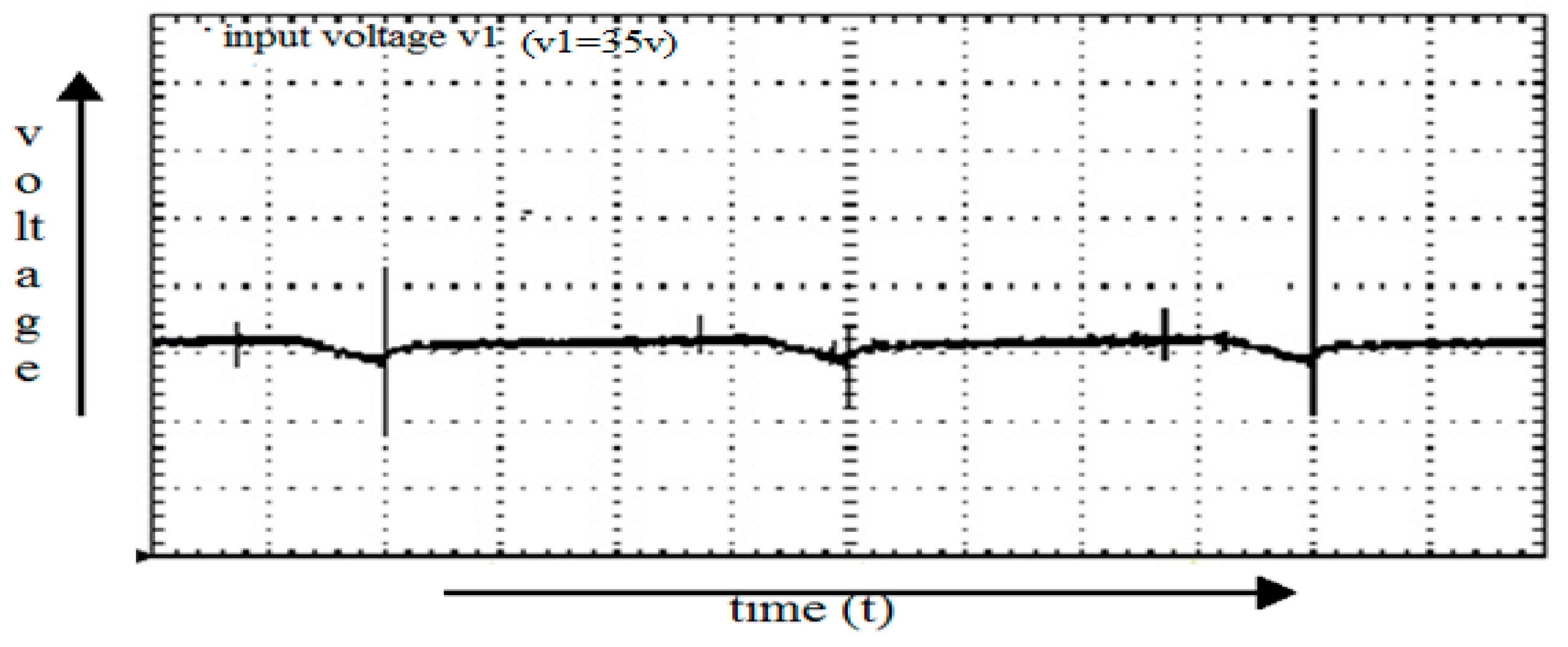
Figure 32.
Input voltage V1.
Figure 32.
Input voltage V1.
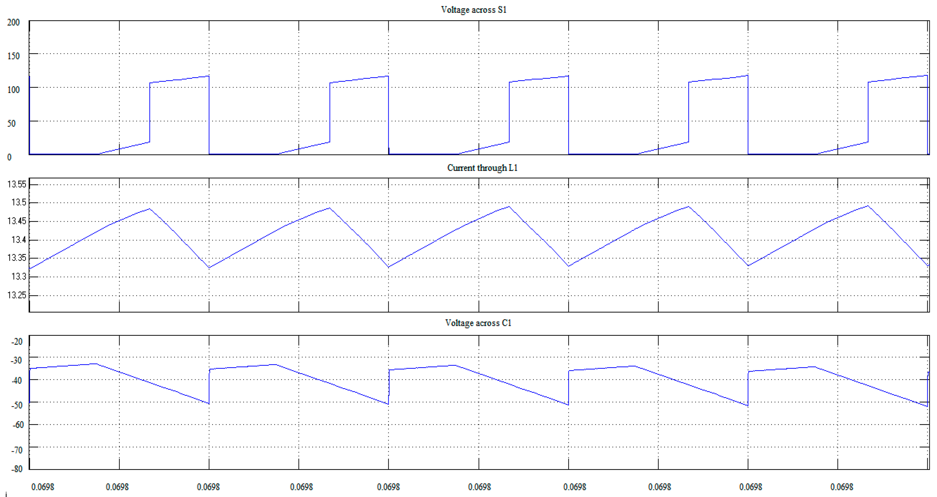
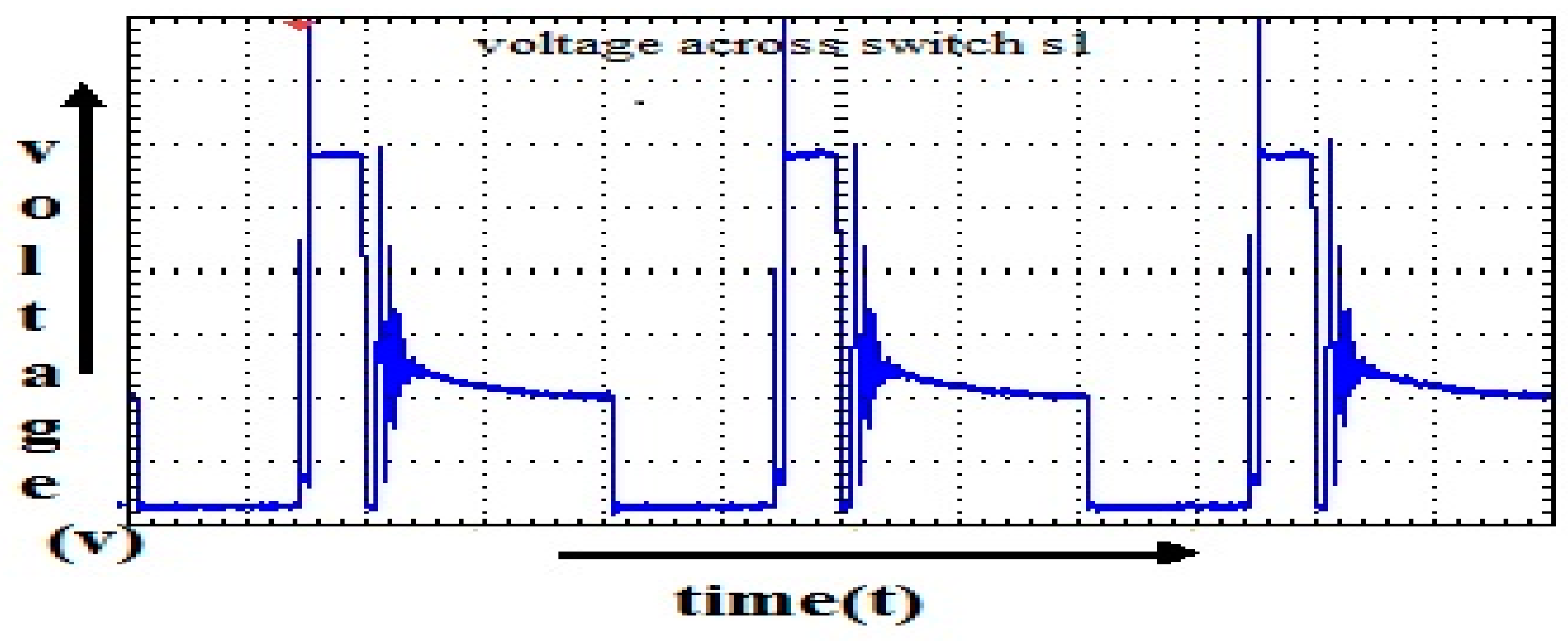
Figure 33.
Voltage across switch S1.
Figure 33.
Voltage across switch S1.
Figure 34.
Voltage across switch S2.
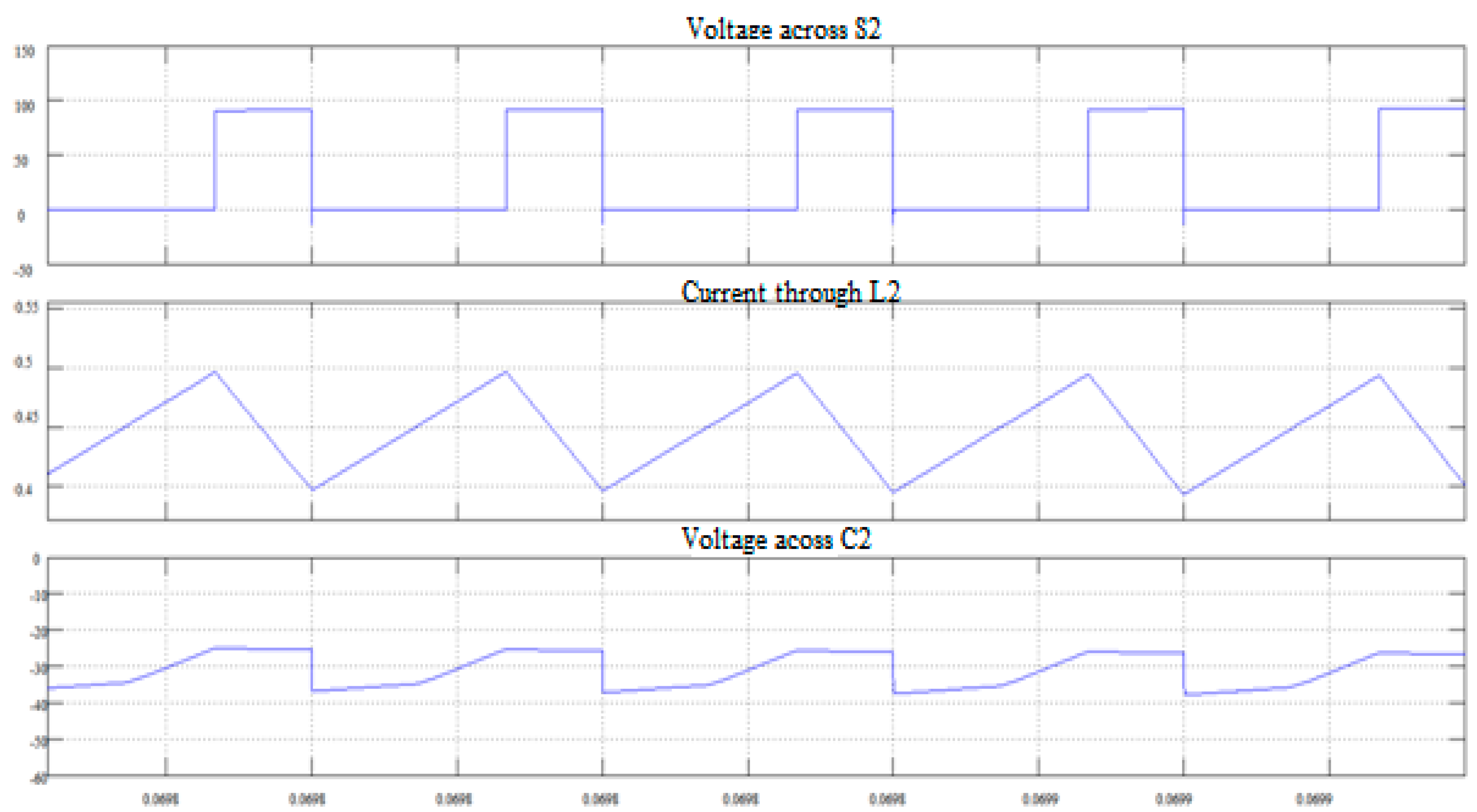
Figure 34.
Voltage across switch S2.
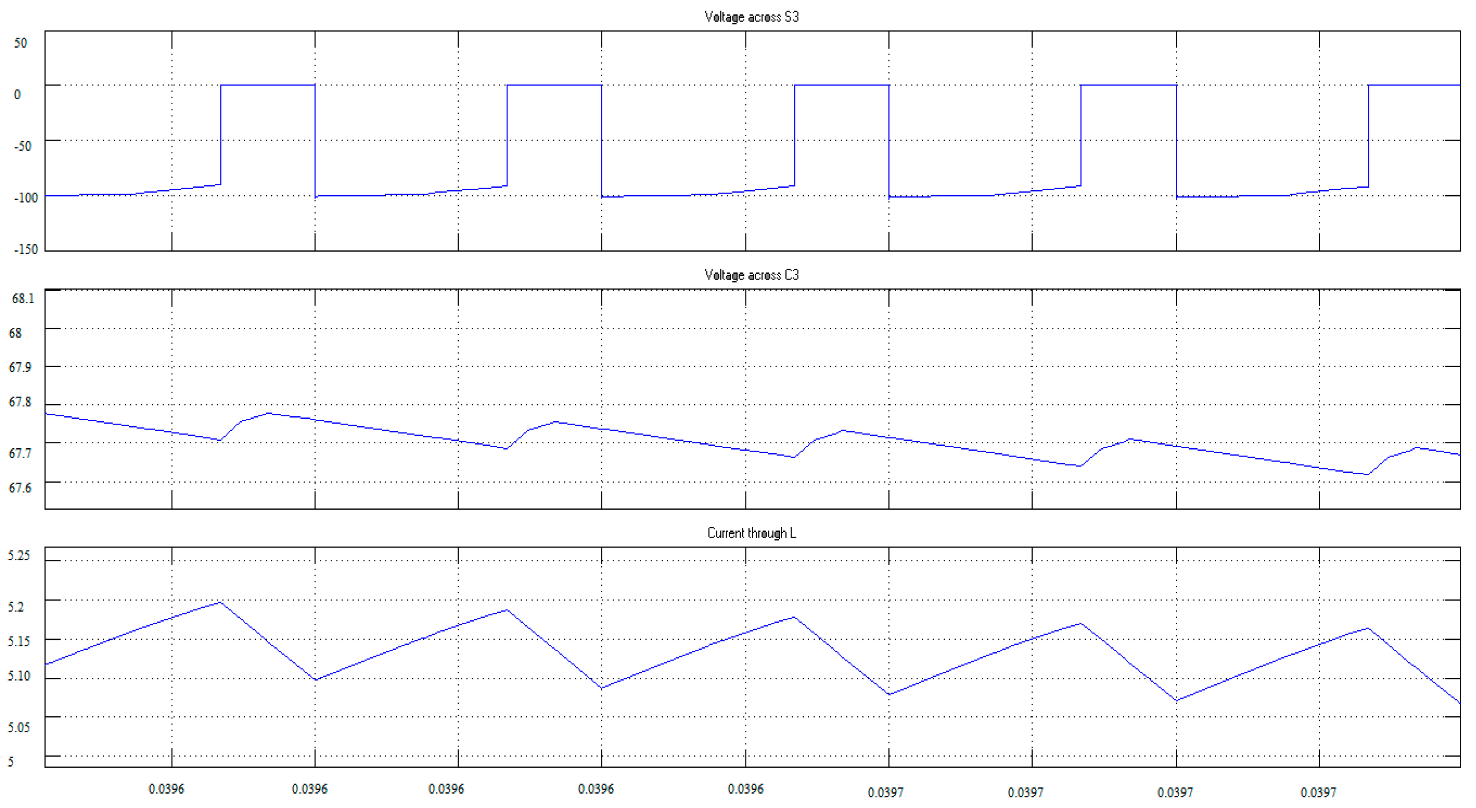
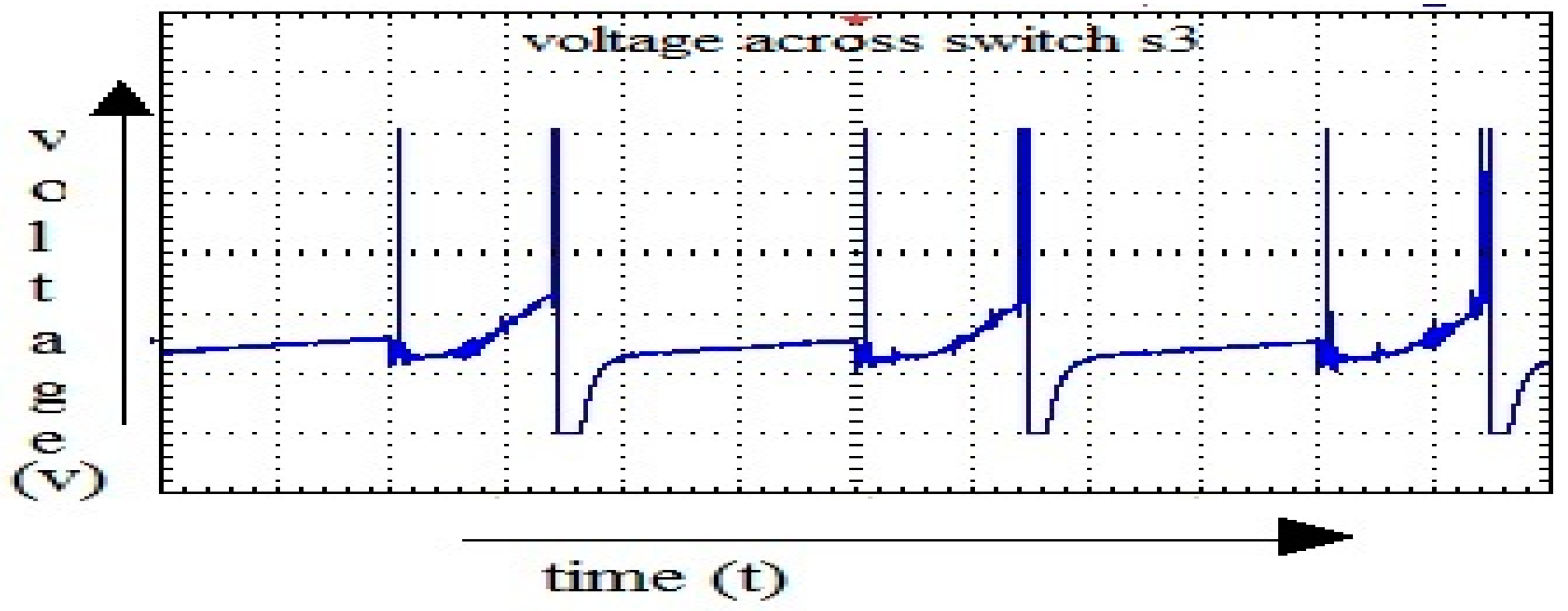
Figure 35.
Voltage across switch S3.
Figure 35.
Voltage across switch S3.
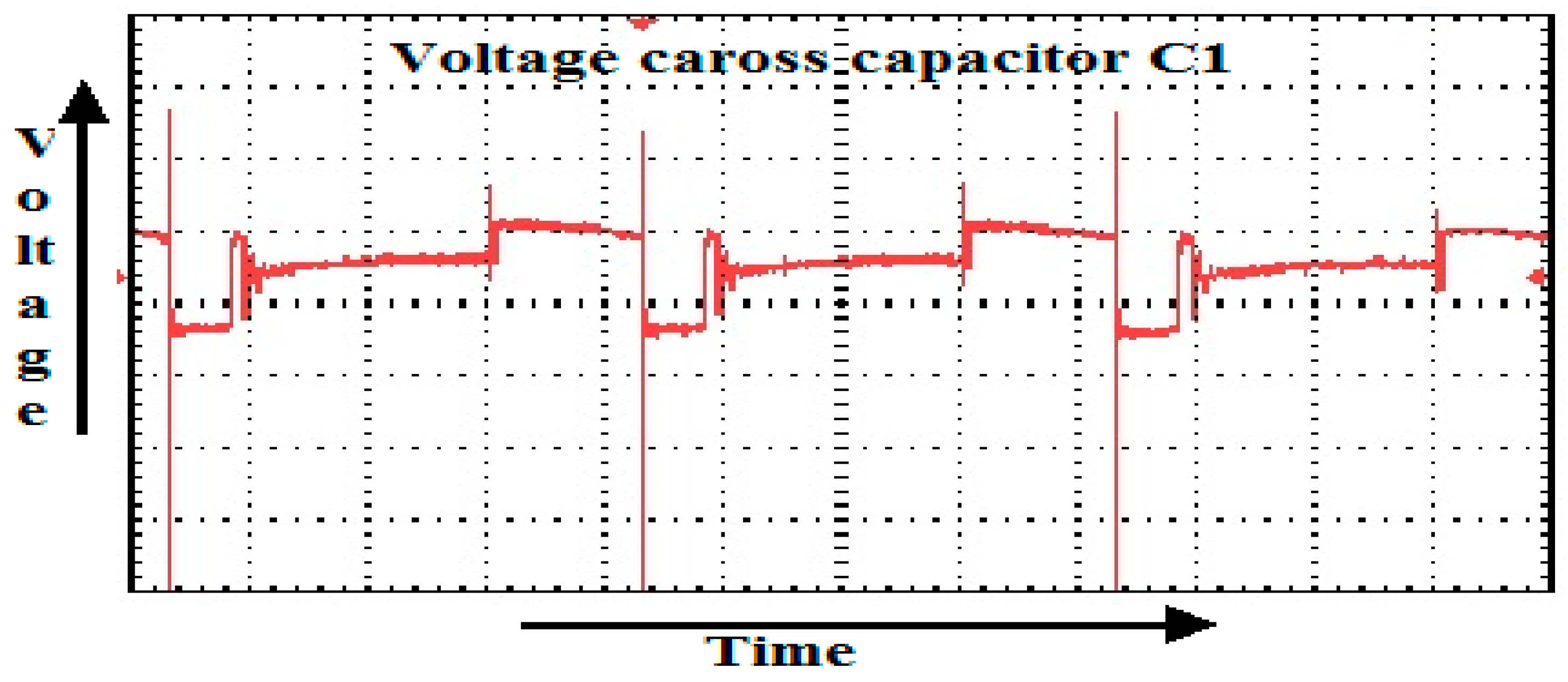
Figure 36.
Voltage across capacitor C1.
Figure 36.
Voltage across capacitor C1.
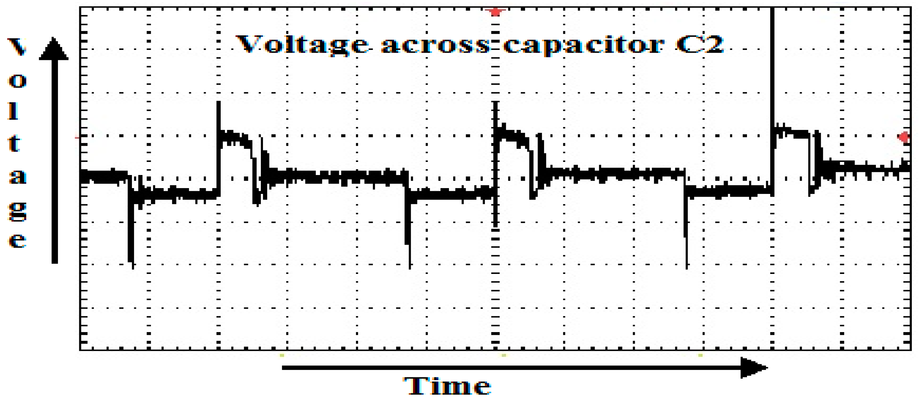
Figure 37.
Voltage across capacitor C2.
Figure 37.
Voltage across capacitor C2.
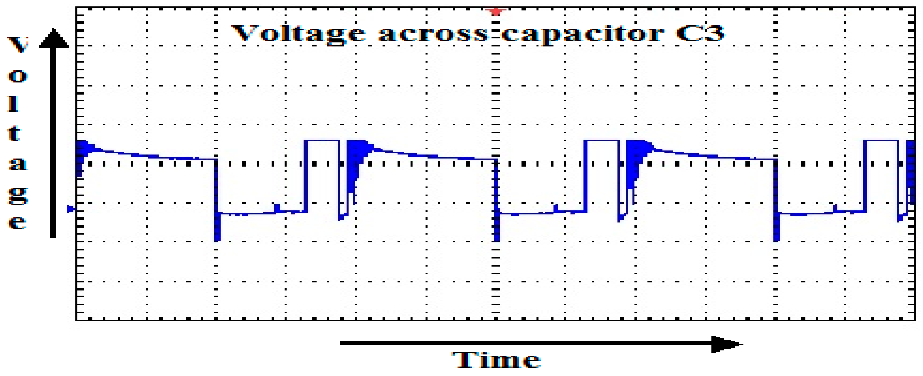
Figure 38.
Voltage across C3.
Figure 38.
Voltage across C3.
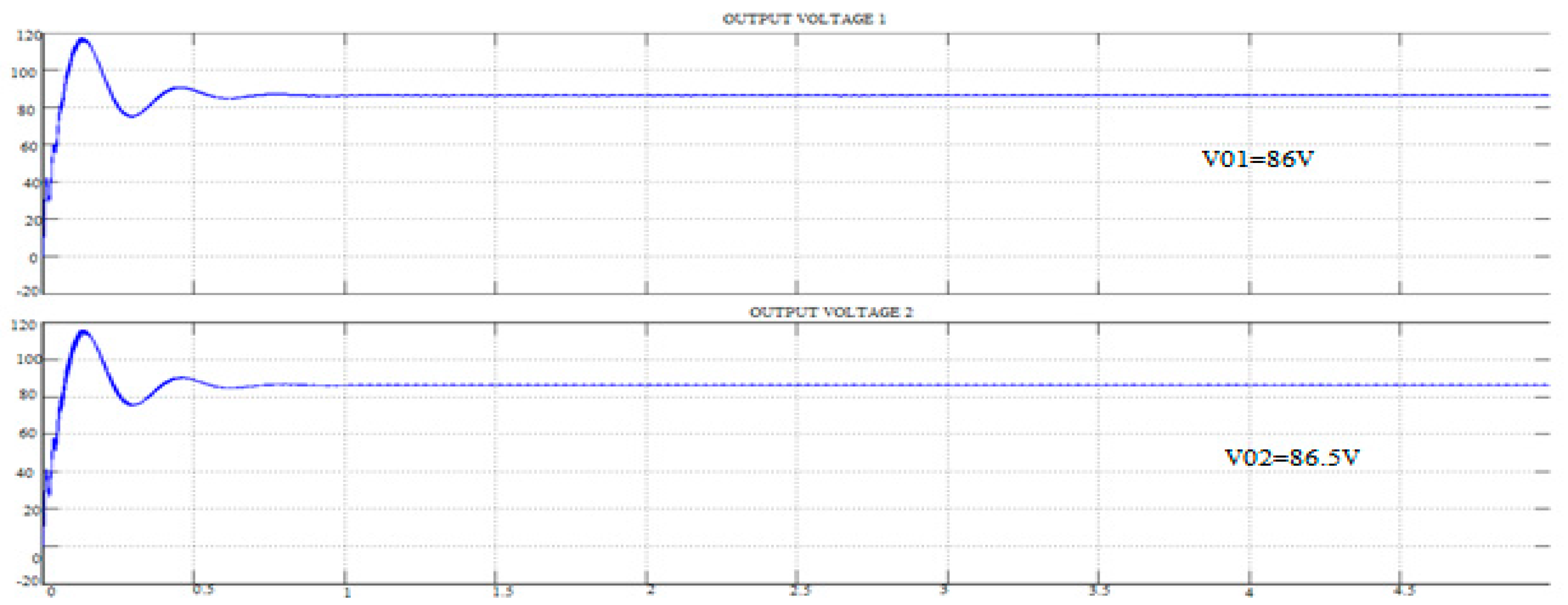
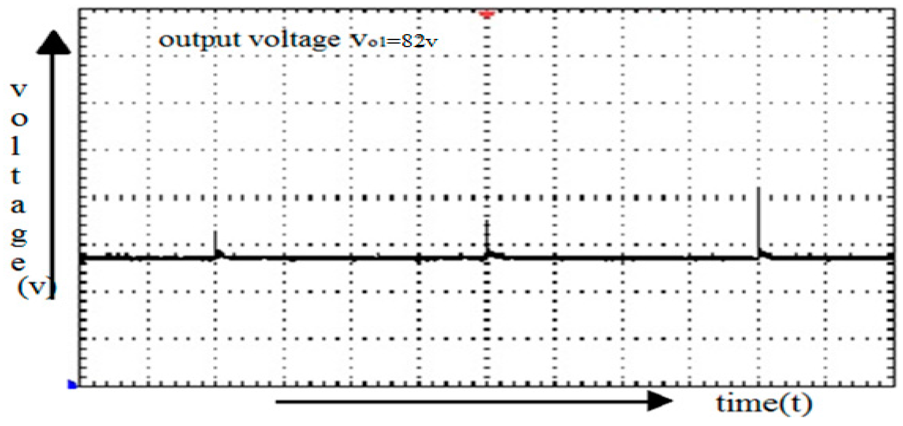
Figure 39.
Output voltage V01.
Figure 39.
Output voltage V01.
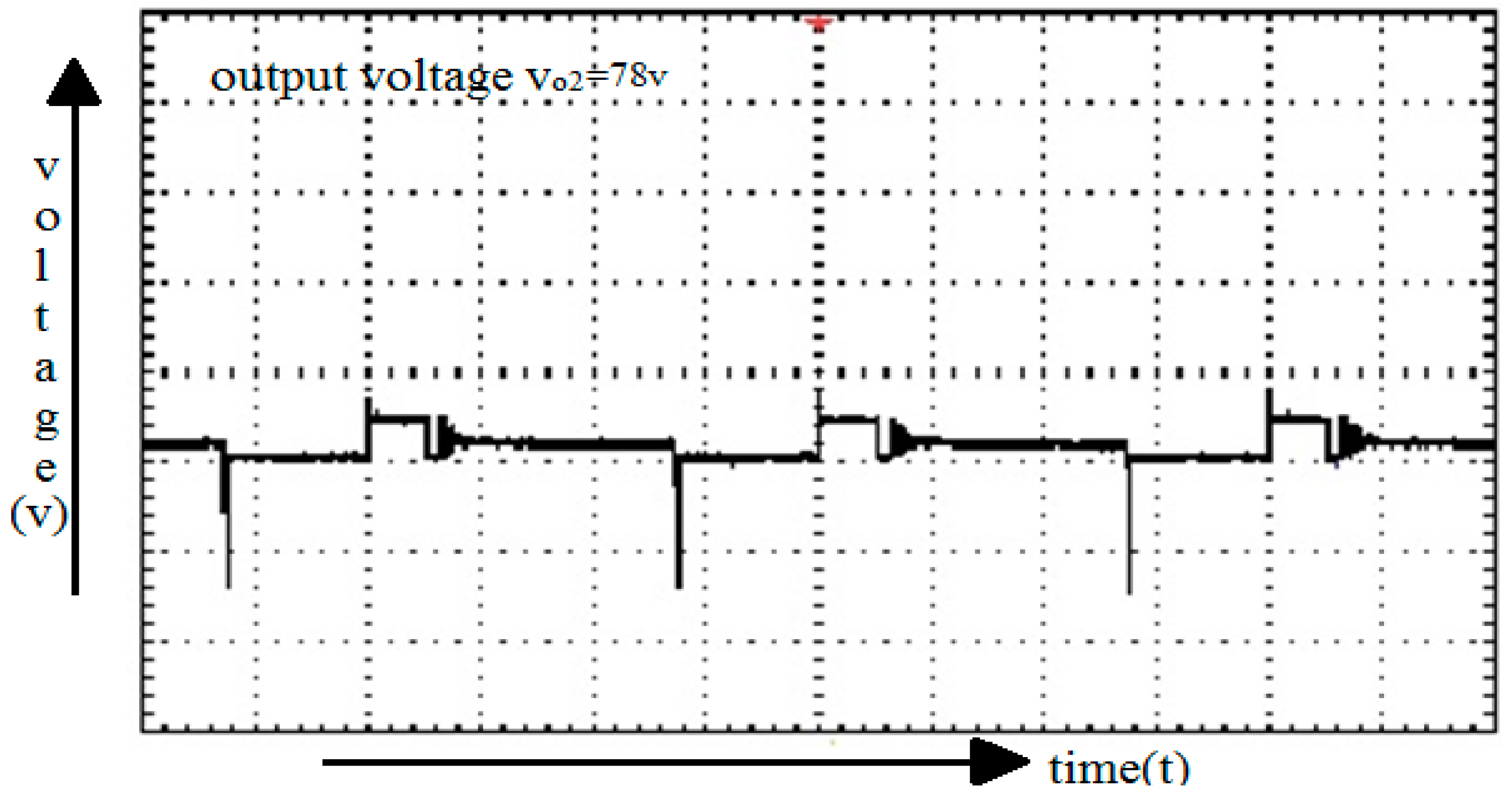
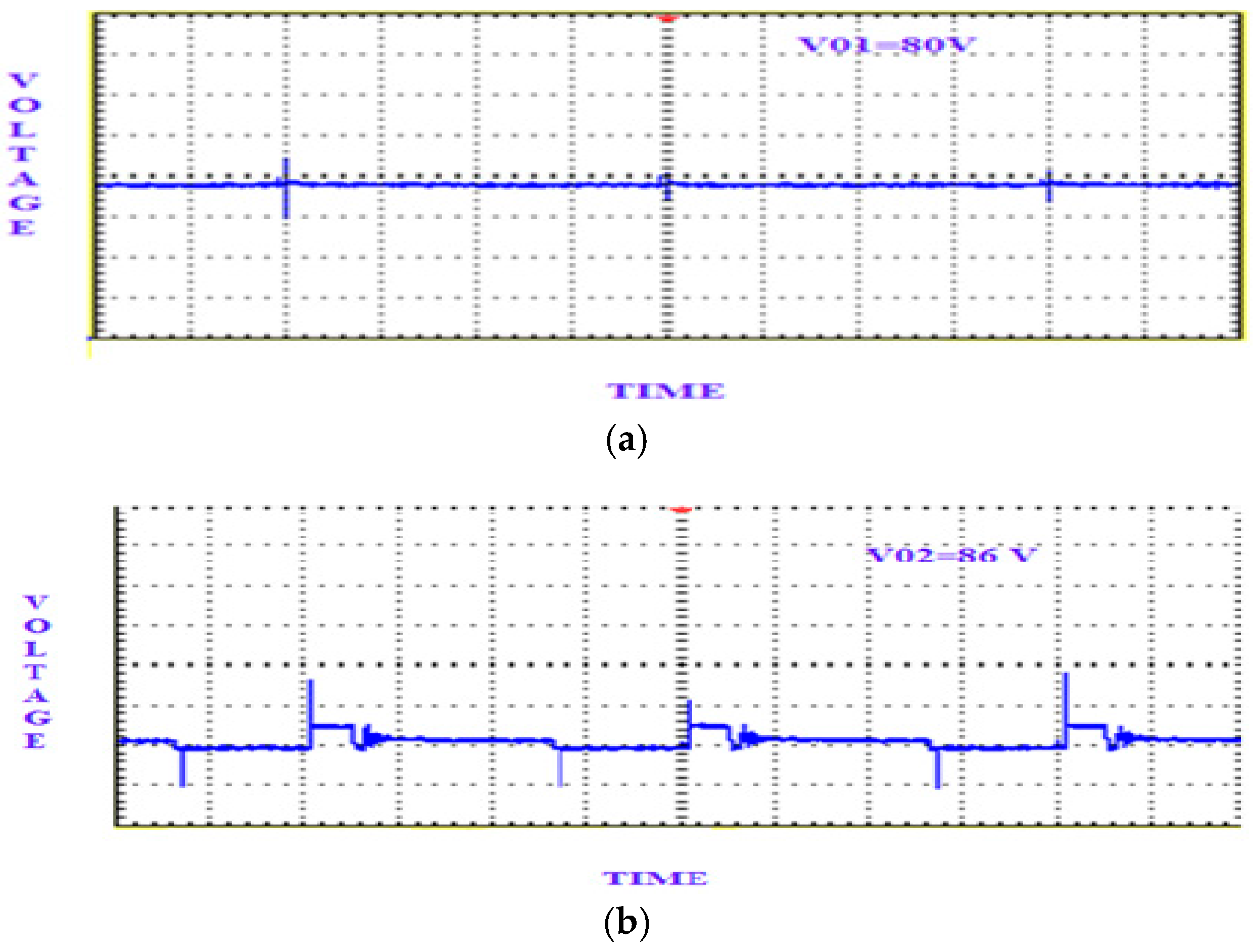
Figure 40.
Output voltage V02.
Figure 40.
Output voltage V02.
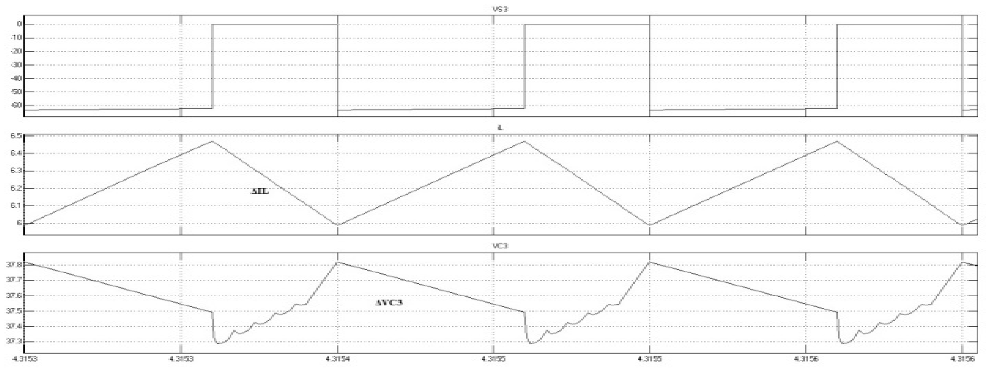
Figure 41.
(a) Ripple waveform for voltage of load 1; (b) Ripple waveform for voltage of load 2.
Figure 41.
(a) Ripple waveform for voltage of load 1; (b) Ripple waveform for voltage of load 2.
Table 1.
Comparison table of components of MPC and MIPC SEPIC.
Table 1.
Comparison table of components of MPC and MIPC SEPIC.
| Components | Multiport Converter | (n) Individual SEPIC Converters |
|---|
| Capacitors | n | 2(n − 1) |
| Inductors | 2 | 2(n − 1) |
| Switches | n | n − 1 |
| Diodes | 0 | n − 1 |
Table 2.
Comparisons of the components in conventional MPC and the proposed SEPIC/SEPIC MPC.
Table 2.
Comparisons of the components in conventional MPC and the proposed SEPIC/SEPIC MPC.
| Components | n Port SEPIC/SEPIC Converter | (n − 2) Individual SEPIC Converter |
|---|
| Capacitors | N | 2(n − 2) |
| Inductors | N | 2(n − 2) |
| Switches | n – 2 | n − 2 |
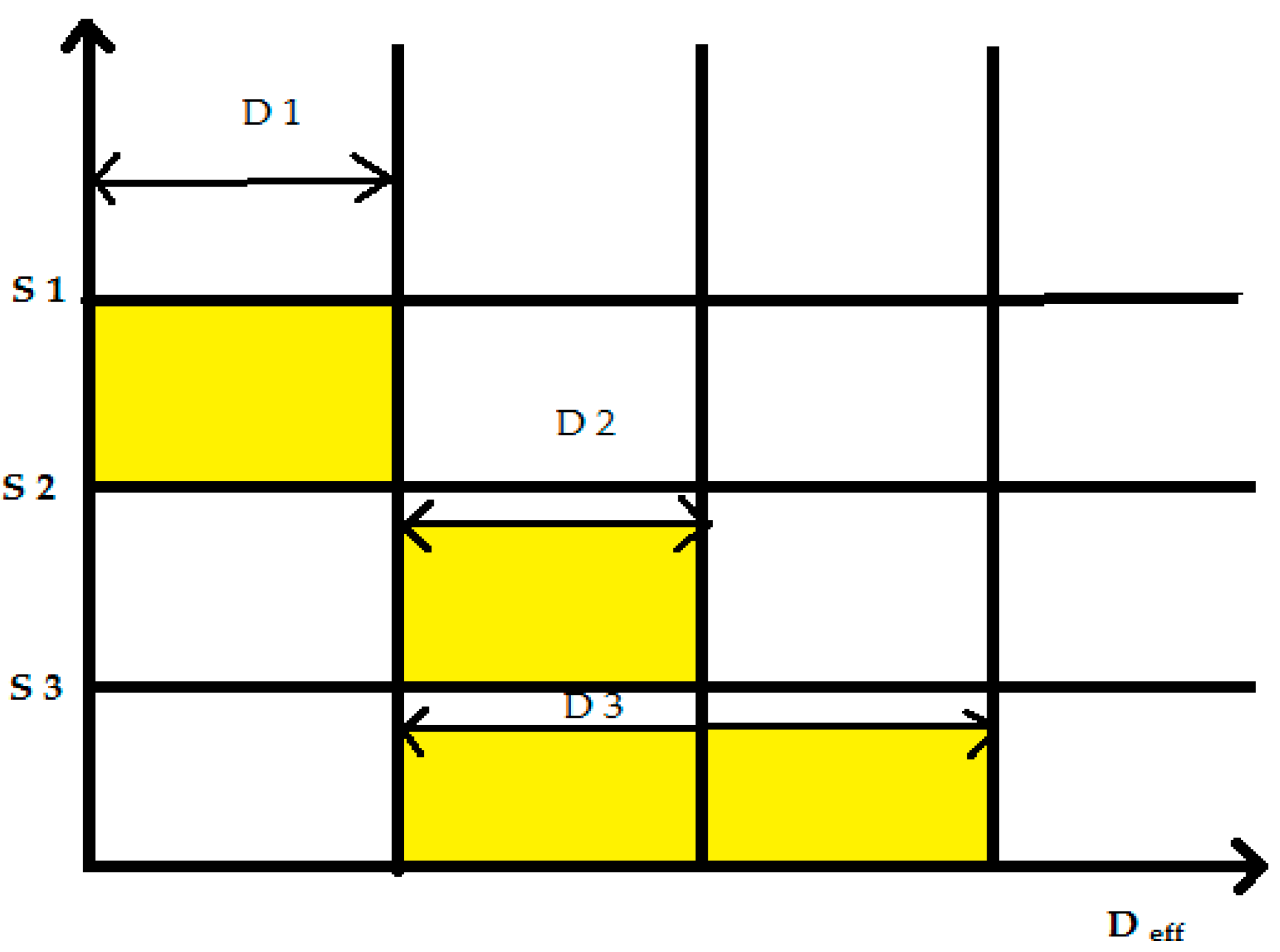
Table 3.
Modes of Operation.
Table 3.
Modes of Operation.
| MODES | ON | OFF |
|---|
| Mode A | S1 | S2, S3, S4 |
| Mode B | S2 | S1, S3, S4 |
| Mode C | S3, S4 | S1, S2 |
| Mode D | S4 | S1, S2, S3 |
Table 4.
Actual and estimated values of output voltage for different set of supplies.
Table 4.
Actual and estimated values of output voltage for different set of supplies.
| V1 | D1 | D2 | D3 | V2 (act) | V2 (est.) | V3 (act) | V3 (est.) |
|---|
| 25 | 60 | 30 | 10 | 37.5 | 35.97 | 37.5 | 35.93 |
| 25 | 50 | 30 | 20 | 25 | 24.63 | 25 | 24.59 |
| 30 | 30 | 20 | 50 | 13 | 12.55 | 13 | 12.51 |
| 30 | 40 | 40 | 20 | 20 | 19.75 | 20 | 19.71 |
| 36 | 60 | 30 | 10 | 54 | 51.8 | 54 | 51.7 |
| 36 | 70 | 20 | 10 | 84 | 78.43 | 84 | 78.29 |
Table 5.
Design of parameters.
Table 5.
Design of parameters.
| PVSC Inductor, L1 | 15 mH |
| Common inductor, L | 15 mH |
| PVSC1 capacitor, C1 | 0.54 mF |
| PVLC1 capacitor, C2 | 0.54 mF |
| PVLC2 capacitor, C3 | 0.46 mF |
| Switching frequency, f | 5000 Hz |
Table 6.
Component specifications.
Table 6.
Component specifications.
| Component | Model | Specification |
|---|
| Microcontroller | DSPIC30F2010 | 28 IC pins |
| 6 PWM channel |
| (21–26) |
| 5 V operating voltage |
| 10 MHz operating frequency |
| (9–10) |
| Driver | TLP250 | 8 pins |
| 12 V operating voltage |
| IGBT | FGA15N120 | 15 A maximum current |
| 1200 V maximum voltage |
| MOSFET | ISA04N60A | 1 MHz maximum frequency |
| 600 V maximum voltage |
| 4 A maximum current |
Table 7.
Actual and Estimated Output Voltages for Different Sets of Input Voltages.
Table 7.
Actual and Estimated Output Voltages for Different Sets of Input Voltages.
| V1 | V2 | D1 | D2 | D3 | D4 | V01 (Act) | V01 (Est.) | V02 (Act) | V02 (Est.) |
|---|
| 50 | 25 | 0.37 | 0.67 | 0.15 | 0.33 | 80 | 79 | 80 | 78.78 |
| 50 | 35 | 0.25 | 0.70 | 0.15 | 0.30 | 95 | 94.17 | 95 | 94.16 |
| 60 | 30 | 0.20 | 0.50 | 0.30 | 0.50 | 45 | 42 | 45 | 42 |
| 60 | 40 | 0.42 | 0.60 | 0.25 | 0.40 | 82 | 81 | 82 | 81 |
| 35 | 20 | 0.30 | 0.55 | 0.20 | 0.45 | 32.5 | 34.45 | 32.5 | 34.44 |


