Article

Design of Low-Ripple and Fast-Response DC Filters in DC Distribution Networks

State Key Laboratory of Power Transmission Equipment & System Security and New Technology, Chongqing University, Chongqing 400044, China
*
Author to whom correspondence should be addressed.
Energies 2018, 11(11), 3128; https://doi.org/10.3390/en11113128
Submission received: 28 September 2018 / Revised: 9 November 2018 / Accepted: 9 November 2018 / Published: 12 November 2018
(This article belongs to the Special Issue Operation and Control of Power Distribution Systems)

Abstract

:
The design and parameter selection of low-ripple and fast-response direct current (DC) filters are discussed in this study with the aim of alleviating the influence of a DC-side low-frequency voltage pulsation on a sensitive load in a DC distribution network. A method for determining the DC filter parameters by using a mofatching most flat response algorithm is presented. The voltage transfer function of the DC-side filter in the DC distribution network is deduced to analyze its voltage transfer characteristics. The resonance peak value of the filter network is an important factor affecting the transfer speed of a filter. A pole-circle-based parameter optimization method is proposed to move the poles of the filter transfer function down and to the left of pole plane for finding the appropriate capacitance, inductance, and damping parameters. This approach effectively restricts the resonance peak value, accelerates the transfer speed, and maintains steady filtering results. Simulation and test results verify that the filter has low resonance value, rapid convergence ability, and an excellent filtering effect.

1. Introduction

Considering the increasing use of distributed generation, electric vehicles, energy storage, and energy efficient loads that generate or consume direct current (DC) power, DC distribution networks offer a promising alternative to their alternating current (AC) counterpart [1,2,3,4]. The improved compatibility between DC devices and a DC power backbone reduces and simplifies the power conversion steps, thereby reducing power conversion losses and increasing the component-level reliability [5,6,7,8]. However, similar to the AC distribution network, DC distribution networks with intermittent renewable energy sources (RES) and variable load demands cause power imbalances and subsequently generate a voltage variation in the DC bus [7,8,9,10]. A large variation in the DC link voltage can lead to the efficiency and performance degradation of its downstream converters [11], and increased voltage stresses of the system [12] and interference between the DC and AC utilities due to the coupling effect. For specific applications, this variation can also generate undesirable flickers in light emitting diode (LED) lighting [13], decrease the operating lifetime of batteries [14], and diminish the power efficiency of photovoltaic (PV) panels [15]. A large voltage ripple across the electrolytic capacitor (E-cap) leads to a massive capacitor current ripple, increasing the internal resistive loss and temperature inside the E-Cap [16].
In view of these challenges, there is a growing interest in using DC filtering approaches to stabilizing the DC-link voltage [17,18]. DC filtering research for DC distribution networks has aimed to diminish the DC voltage modulation harmonics and suppress the possible low-frequency pulsation in the system. Currently, the available DC filtering methods for DC distribution networks are divided into two categories: active power filtering (APF) [19,20,21,22,23] and passive power filtering (PPF) [24,25,26,27,28,29]. APF can eliminate DC voltage fluctuation dynamically by paralleling the voltage converter on the DC side. For example, Wang et al. [20] proposed eliminating harmonics in the DC bus voltage with a DC electric spring. This approach adjusts the consumption power of a non-critical load to make it follow the power variation of renewable energy. However, the ability of this method to eliminate voltage harmonics is limited considering the restricted power of non-critical loads. In Li et al. [19], a pluggable voltage pulsation suppression device was designed to realize flexible control of the voltage ripple in an AC/DC hybrid distribution network. However, adding a device at each node evidently increased the cost of investment. Lee et al. [21] suggested suppressing DC voltage pulsation using an energy storage device in the DC distribution network and controlling the converters. However, the control method is complex and the operation and maintenance costs of the energy storage device are high. In Li et al. [23], a ripple eliminator, which is a bidirectional buck-boost converter terminated with an auxiliary capacitor, was adopted to replace bulky capacitors in DC systems. Although the APF is effective at eliminating voltage harmonics, designing and controlling DC APF is complex and costly [22]. In addition, APF is rarely used in DC distribution networks with large capacity and high voltage given its limitations. The DC passive filter design is simple without the additional of a controller, acting as the main DC voltage filter in the DC distribution network. DC passive filters are mainly divided into tuned and low-pass filters. The former has a large occupational area and minimal flexibility [27]. The latter can filter the harmonics after a cut-off frequency. However, the particularly small cut-off frequency enlarges the parameters of inductance and capacitance, thereby affecting the dynamic response characteristics of the DC distribution system and limiting the power transmission capacity [24]. Thus, Beres et al. [24] designed a bidirectional low-ripple and fast-response low-pass filter using the Chebyshev algorithm to diminish the value of the DC-side smoothing reactor and increase transmission capacity. However, the designed five-order Chebyshev filter (CBSF) required highly accurate element parameters, which could not be matched in practice. To solve this problem, Kang et al. [28] designed a four-order flat response filter (FRF) with standard element values and optimized the element parameters of the filter with the evolutionary algorithm, thereby diminishing the deviation between the designed and the actual element parameters of the filter; however, the parameter selection process was complex and increased the response time of the DC voltage.
In the present study, a low-ripple and fast-response DC filter for DC distribution networks is designed using a matching most flat response algorithm. This algorithm integrates the parameters of the filter with the fluctuation characteristics of the DC voltage in the DC distribution network. In Section 2 the applications, frequency response characteristics, and response speed of all kinds of filters are analyzed. FRF was selected as the basic prototype to design the filter. Then, the order of the filter was determined in accordance with the requirements of the dynamic frequency response characteristics of the filter. The element parameters of the filter were selected using the matching design algorithm in accordance with the equivalent impedance on both sides of the filter. Section 3 outlines the derivation of the voltage transfer function of the DC filter network and the further optimization of the parameters of the filter through a pole-circle-based parameter optimization method. The optimized filter further restricts the resonant peak value and accelerate transfer speed. Section 4 details the filtering and response time simulations on the designed filter through bipolar and single-ended radial DC distribution networks, respectively. Finally, an experimental analysis is conducted on the designed filter by creating an experimental platform for a radial DC distribution network.

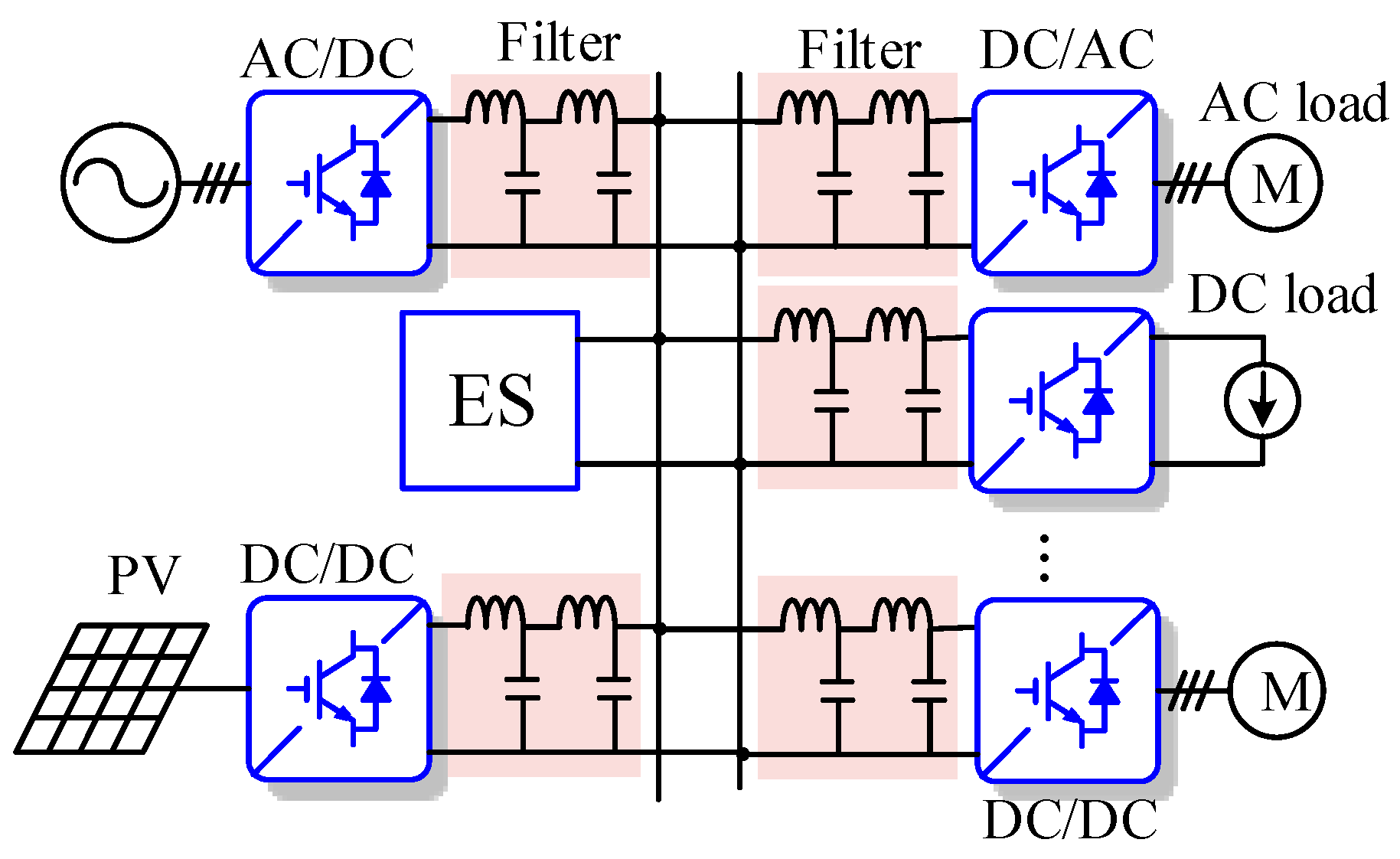
2. Design of DC Filters for DC Distribution Networks

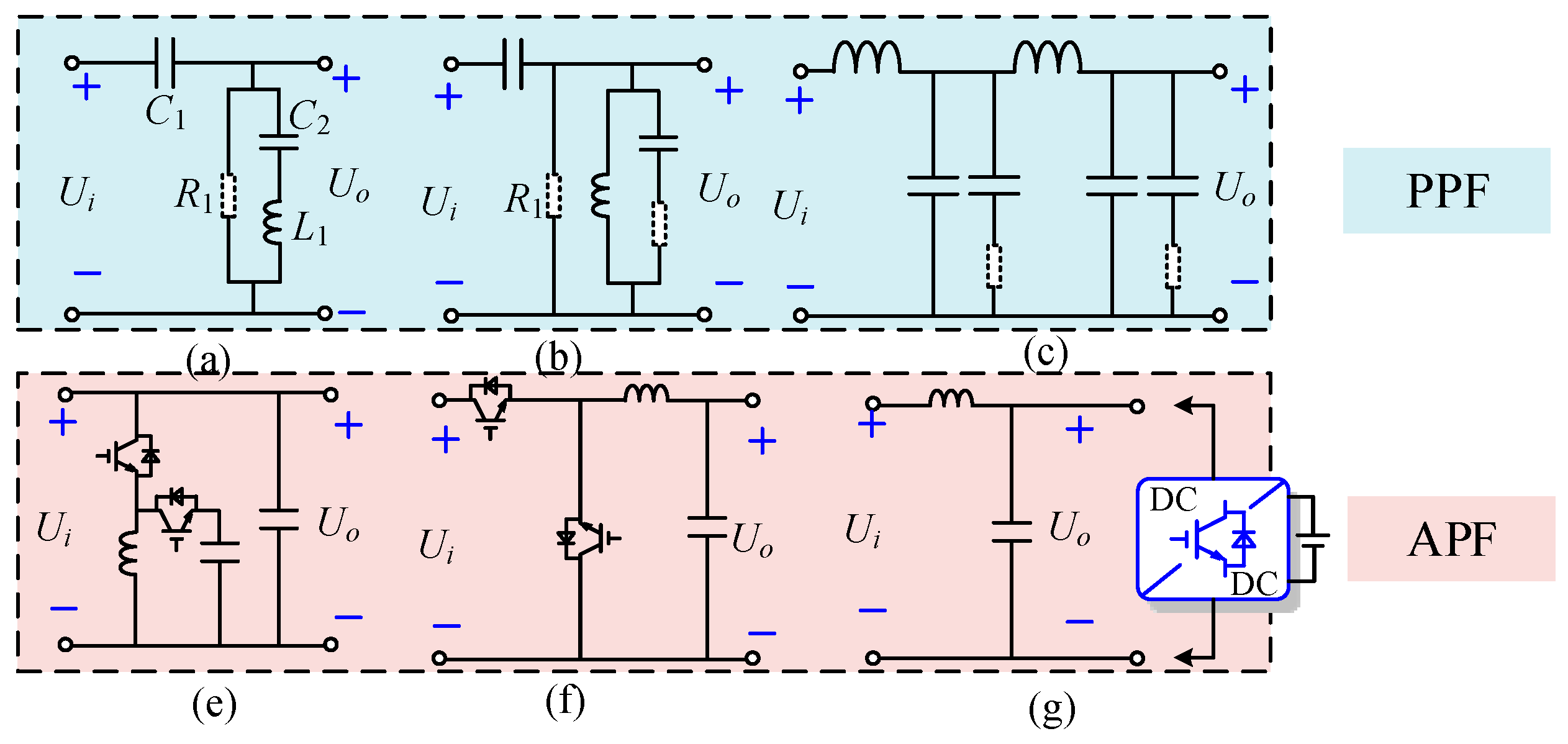
2.1. Basic Prototype Selection of DC Filters

The basic structure of six kinds of filters is illustrated in Figure 1 to clearly demonstrate the current design status of DC filters. Figure 1a–c depict a double-tuned high-pass filter, C-type filter, and six-order damping-CBSF, respectively. Figure 1e–g show the basic structure of the APF. The APF reduces the volume of the DC-side filter (especially for capacitors) by introducing a full-control device and adding ripple suppression control to the AC/DC or DC/DC converter. However, the capacity of the APF is limited for high-voltage DC distribution networks. For high-voltage and large-capacity applications, PPF design is a focus among researchers. Aleem et al. [30,31] adopted an optimization algorithm to enhance the parameters of the tuning filter (TF). The designed filter is optimal in terms of coverage area and filtering effect, but the accuracy of its component parameters could not be achieved in practice. To increase PV hosting capacity in distorted distribution systems, Sakar et al. [32] designed a C-type passive filter (Figure 1b) to maximize the harmonic constraint, but the filter design method is not presented. Ali et al. [33] developed a new multiple-arm passive filter design method on the basis of a crow search algorithm to minimize the total harmonic current distortion as an objective function for an industrial plant. Zhang et al. [34] designed a six-order damping-CBSF (Figure 1c), which accelerates the response speed of the DC filter system, but the design parameters of the filter are numerous and require high precision. In this study, a two-stage LC filter (LCF) structure is proposed. The parameters of the filter are designed using the matching most flat response algorithm and optimized on the basis of the pole-circle-based method, which is different from the traditional LC filtering scheme.
Different filters have corresponding applications, advantages, and disadvantages, as summarized in Table 1. In this table, APF with complex design, control, and high cost has certain limitations in being applied to DC distribution networks. Passive filters are suitable for DC-side filtering of the DC distribution network considering the simple principle and low cost. The frequency response characteristics of four passive filters are displayed in Figure 2a,b. The TF can only filter out a specific order of harmonics, which is unsuitable for the DC distribution network with substantial spectra in the DC voltage. LCF has a favorable filtering effect for high-frequency pulsations, but its volume must be increased for low-frequency pulsation elements, such as the second harmonic, and its lifetime is affected by the second harmonic content. The curves of the response time and attenuation of the harmonic content with passbands of CBSF and FRF are presented in Figure 2c,d, respectively, whose data were obtained through experiments. In these figures, the FRF has a rapid response time and low harmonic content under the same passband attenuation [1]. Therefore, the FRF was selected as the basic filter design prototype in this study. On this basis, the FRF parameters were optimized to suppress low-frequency pulsations and accelerate the transfer speed of the filter.

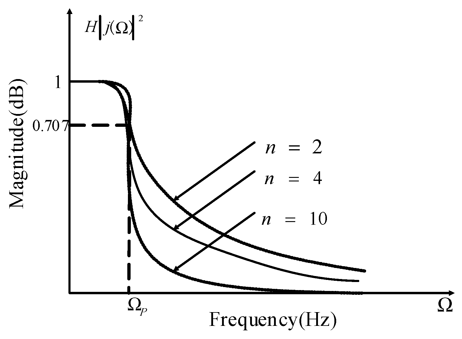
2.2. Design and Characteristic Analysis of DC Filters

The FRF has the most flat frequency response characteristics for the filter passband to restrict the resonance peak value and accelerate the transfer speed. Therefore, applying FRF in a DC distribution network has unique advantages. The use of FRF to filter the DC bus voltage in a DC distribution network can decrease the volume of the filter capacitor and inductor. The structure and installation position of the FRF in the DC distribution network are illustrated in Figure 3.
The modular square transfer function and attenuation characteristics of the matching most flat response algorithm satisfy Equations (1) and (2) [34]:
| H | 2 = 1 + ε 2 ( Ω s Ω p ) = 1 + ε 2 Ω 2 n
α ( Ω ) = 10 lg 1 | H ( j Ω ) | 2 = 10 lg ( 1 + C 2 Ω 2 n )
where n is the order of the filter; Ωp and Ωs are the frequencies of the passband and stopband, respectively; Ω = Ωs/Ωp is the normalized frequency; ε = 1/(ρ−2 − 1)0.5; ρ is the reflection coefficient of the filter; and C is the auxiliary constant designed by the filter. According to Equations (1) and (2), the characteristic curve of the attenuation of the FRF passband that varies with the order can be obtained, as depicted in Figure 4. In this figure, the order of the filter significantly influences the attenuation characteristics. Thus, determining the order of the filter is necessary.
The order of the filter is determined by its passband and stopband frequencies and their attenuation values. A high order of the filter indicates the high accuracy of the element parameters. Therefore, the order of the filter is as small as possible because the filtering effect is satisfied. The selected frequency of the passband is 50 Hz, and the selected stopband attenuation ( α s ) is 20 dB, given the low-frequency pulsation of the DC voltage given the three-phase unbalance of the AC grid. Our purpose was to filter the voltage pulsations with the second frequency and above. The calculation equation of the FRF order is [35]:
n lg ( 10 0.1 α s ) ( 1 ρ 2 1 ) lg Ω s
The aforementioned parameters are substituted to the equation to obtain the order of the designed filter. In the present study, three parameters were considered. The frequency characteristic curve of the third-order FRF was drawn in MATLAB (MathWorks, Natick, MA, USA), as demonstrated in Figure 5. The filter attenuated for 3 dB at 50 Hz and 18 dB at 100 Hz. This process was consistent with the design intention. After determining the order of the filter, the FRF of the π-type structure was selected, and its structure is exhibited in Figure 6. In this figure, L1 is the smoothing reactor. The L1 should have a small value to ensure the dynamic performance of the system. Here, the L1 value was temporarily taken as 20 uH. L2, C1, and C2 were the basic parameters of the π-type FRF; R L 1 and R L 2 and R C 1 and R C 2 were the damping parameters in the inductance and capacitance branches, respectively. The inductance and capacitance currents were i L 1 and i L 2 and i C 1 and i C 2 , correspondingly; the input and output voltages of the port were Ui and Uo, respectively; and the equivalent impedance variables of the input and output were Ri and Ro, correspondingly.
The matching most flat response algorithm was used to select the element parameters. This method aimed to balance the equivalent impedance of the connected systems on both filter sides. According to the matching most flat response algorithm, the normalized element parameter km of the filter can be calculated using the following equation [35]:
k m = 1 C [ 2 sin ( 2 m 1 ) π 2 n ]
where m is a natural number. When m is odd or even, km is the value of capacitance or inductance, respectively. In accordance with Equation (4), solving the auxiliary parameter C of the filter is necessary. The modular square transfer function of the matching most flat response algorithm at the frequencies of Ω p and Ω s can be obtained using Equation (1), as expressed in Equation (5). C can be obtained using Equation (6). Thus, the value of C depends on the passband attenuation αp. Generally, αp = 3 dB; thus, C = 1.
The voltage and load side impedance of the DC filter directly determines the parameters of the filter. The fundamental frequency of the AC system was set to fc, and the equivalent impedance of the grid and load sides were set to R s and R L , respectively. The benchmark values of resistance, inductance, and capacitance of the filter were set to R0, L0, and C0, correspondingly. The normalized parameters of the filter inductance and capacitance are C ¯ m and L ¯ m , respectively, where m is a natural number. In the matching algorithm, R s = R L = R0 was satisfied. For analysis convenience, the variables were temporarily set to 1 Ω. The actual inductance and capacitance values were the product of the normalized and reference parameters (i.e., L m = L 0 L ¯ m and C m = C 0 C ¯ m ). Thus, the actual parameters of the 3rd-order FRF are calculated as follows [35]:
{ C 2 Ω p 2 n = 10 α p / 10 1 C 2 Ω s 2 n = 10 α s / 10 1
C 2 = 10 α p 10 1
On the basis of the calculation of the normalized element parameter km, when the element is the capacitor or inductor, km = 1 or km = 2, correspondingly. Generally, the parameters of L1 are selected in accordance with the continuous current requirement of the DC bus in the DC distribution network. For the line-commutated converter, the parameters of L1 should satisfy Equation (7), where U d 0 is the no-load voltage, k0 is 0.064 for the six-pulse converter, α is the trigger angle ω = 314 rad/s, and I d j is the minimum load current. For a 480 V, 10 kW DC distribution network, the appropriate value of L1 is 20 mH. According to the results of Equations (7)–(9), the parameter values of the filter could be obtained as listed in Table 2.
L 1 U d 0 k 0 sin α / ω I d j
L 0 = R 0 / 2 π f c
C 0 = 1 / R 0 2 π f c

3. Parameter Optimization and Performance Analysis of the Filter Networks

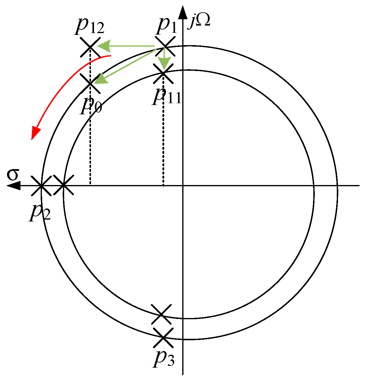
3.1. Optimization of Filter Parameters Based on Pole-Circle

In Equation (1), the n-order matching FRF has 2n poles, which are uniformly distributed on the circle with the radius of Ω. When the parameters are normalized, Ω = 1. The real and imaginary parts of the pole in the s-plane are set to σx and Ωx, respectively. Thus, the coordinates of the pole satisfy Equation (10). Only the n poles on the left half of the s-plane are obtained, that is, p11, j1), p22, j2), …, pnn, jn). The pole distribution of the 3rd-order FRF designed in the present study is displayed in Figure 7:
σ x 2 + Ω x 2 = Ω 2
The capacitance branch presented in Figure 6 is connected in series with a damping resistance. The filter with damping resistance on the capacitance branch is known as a damped FRF (DFRF). The dissipation factor of the capacitor at the normalized frequency was set to. Thus, the normalized admittance of the capacitance branch was:
Y ( j ω ) = C ¯ m [ j Ω + Ω 2 d ( 2 d + 1 ) ] = C ¯ m ( j Ω + d )
Given that Ω2 ≥ 0, Ω’ ≤ Ω. Therefore, the damping resistance in the capacitance branch reduced the passband frequency of the FRF. In Figure 7, the damping resistance enabled the original poles to shift to the left. For example, the change trajectory of Pole 1 was p11, j1) → p1212, j12).
For the DC filter network, the voltage transfer function reflects the variation in voltage with frequency. According to the filter network structure illustrated in Figure 6, the input and output voltages satisfy the differential equation, as expressed in Equation (12). The voltage transfer function of the filter network can be derived from Equation (12), as defined in Equation (13):
{ U i = L 1 d i L 1 d t + 1 C 1 i C 1 d t + i L 1 R L 1 + i C 1 R C 1 U o = 1 C 1 i C 1 d t + i C 1 R C 1 L 2 d i L 2 d t i L 2 R L 2 i L 1 = i C 1 + i L 2 i L 2 = i C 2
G ( s ) = U o ( s ) U i ( s ) = 1 L 1 L 2 C 1 C 2 s 4 + ( L 1 C 1 + L 2 C 2 + L 1 C 2 ) s 2 + 1
When the capacitance and inductance branches in Figure 6 add the damping resistance, the voltage transfer function is described in Equation (14):
U o ( s ) U i ( s ) = s 2 C 1 C 2 R C 1 R C 2 + s ( C 2 R C 2 + C 1 R C 1 ) + 1 s 4 L 1 L 2 C 1 C 2 + s 3 C 1 C 2 ( L 1 R C 1 + L 1 R L 2 + L 2 R L 1 + L 1 R C 2 + L 1 R C 2 ) + s ( R L 1 + R L 2 ) ( C 1 + C 2 ) + s 2 [ C 1 C 2 ( R L 1 R L 2 + R L 1 R C 2 + R L 1 R C 1 + R C 1 R L 2 + R L 1 R C 2 ) + ( L 1 + L 2 ) ( C 1 + C 2 ) ]
In Equation (13), the FRF network has two resonant points, which were also the poles of the filter. The resonant frequencies were set to f1 and f2, and the resonant peaks were obtained at P1 and P2. For the first resonance point f1, s2 = −1/L1C1. At this time, the resonant peak value is:
P 1 = | G ( j 2 π f 1 ) | = C 2 C 1
At the second resonant frequency f2, s2 = −1/L2C2, At this time, the resonance peak value is:
P 2 = | G ( j 2 π f 2 ) | = L 1 L 2
According to Equations (15) and (16), the resonant peak value of the filter was related to the ratio of the passive device parameters. If the parameters of the filter could satisfy C2/C1 < 1 and L1/L2, the attenuation of the FRF at the resonant point was negative, which was beneficial for restricting the resonant peak value of the filter. The present study adopted a decreasing L1 and increasing C1 because the current that flows through C1 was much larger than C2 without changing the parameters of L2 and C2. With the decrease in L1 and the increase in C1, the normalization poles of the filter moved downward in Figure 7 ( Ω = | H | 2 1 / ε , H at Ωp decreased). The pole’s change trajectory was p11, j1) → p1111, j11), thereby indicating a decrease in the radius of the original pole circle. According to the physical meaning of the radius of the pole circle, namely, the normalized cut-off frequency, the method eventually diminishes the passband frequency of the FRF and maintains steady filtering results.
On the basis of the data discussed above, the passband frequency of the filter can be diminished by increasing the damping resistance of the capacitance branch and changing the ratio of inductance and capacitance parameters. The passband frequency would diminish, and the flat response characteristic of the filter would be constant, if the poles are maintained on the pole circle. Finally, the resonant peak of the FRF could be restricted. When selecting the damping resistor and configuring the parameters, the movement of the offset pole p0 ( σ x + Ω 2 d ) / ( 1 + Ω 2 d 2 ) , j Ω x / ( 1 + Ω 2 d 2 ) was downward and to the left along the pole circle, as depicted in Figure 7, because Equation (10) was satisfied. We named the filter optimized by this method the damped non-matching FRF (DNMFRF). The parameters of the filter obtained by the method are listed in Table 3. We found that L1 significantly decreased, which accelerated the filter’s transfer speed.

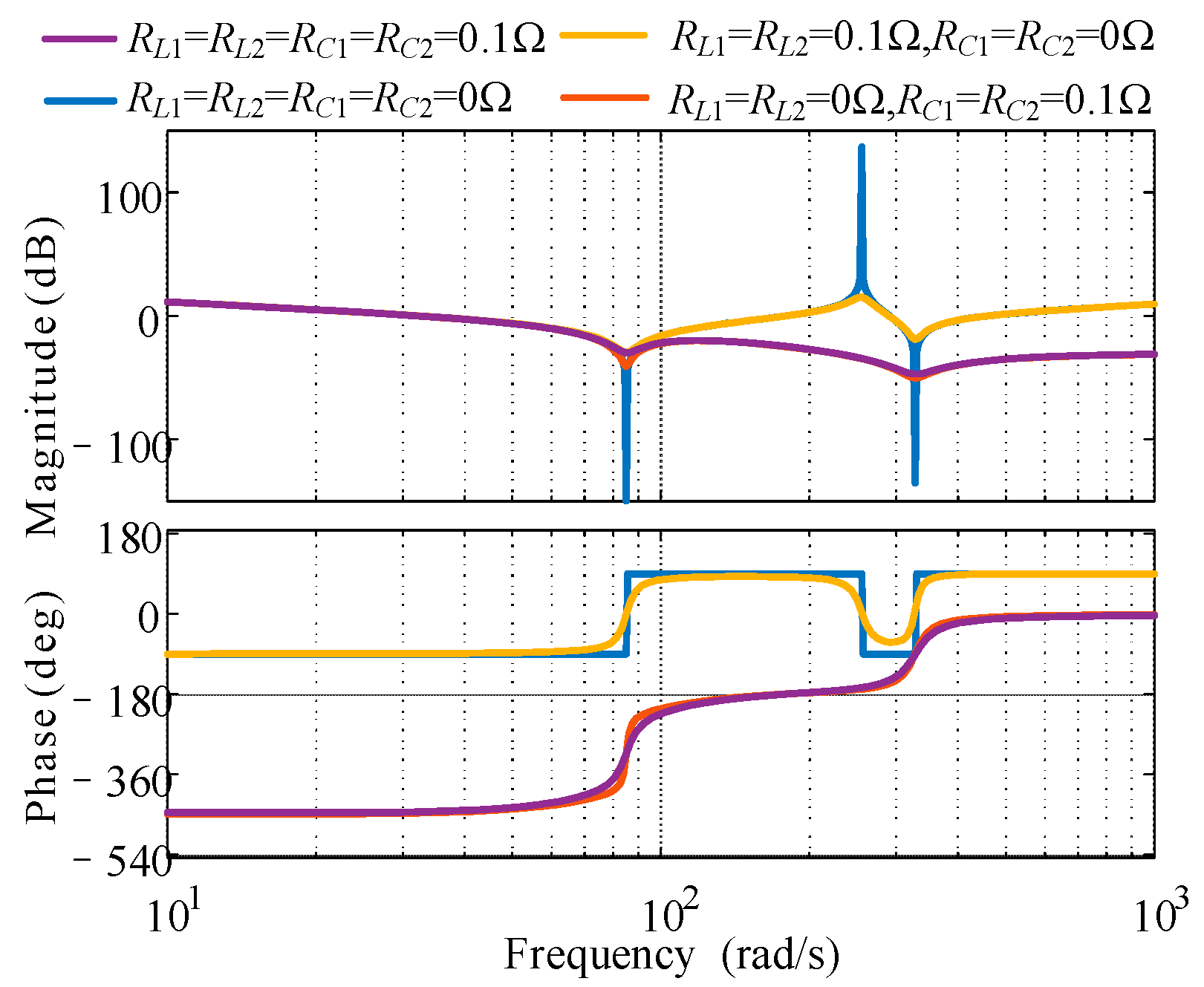
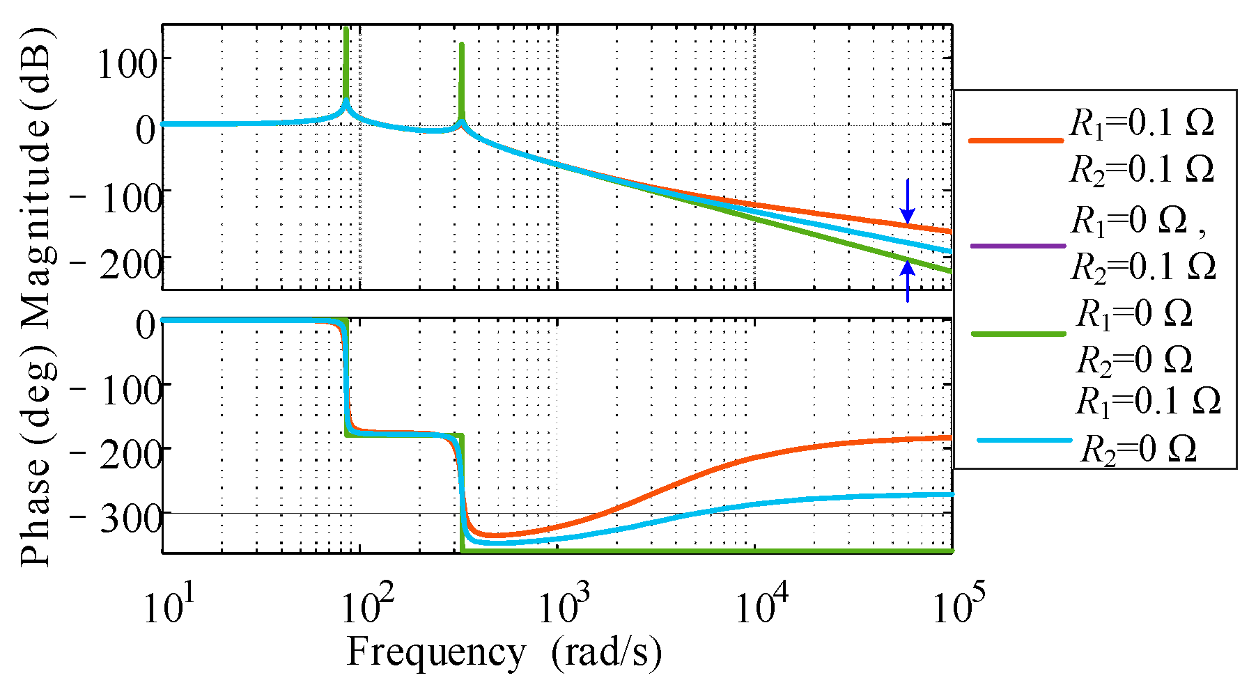
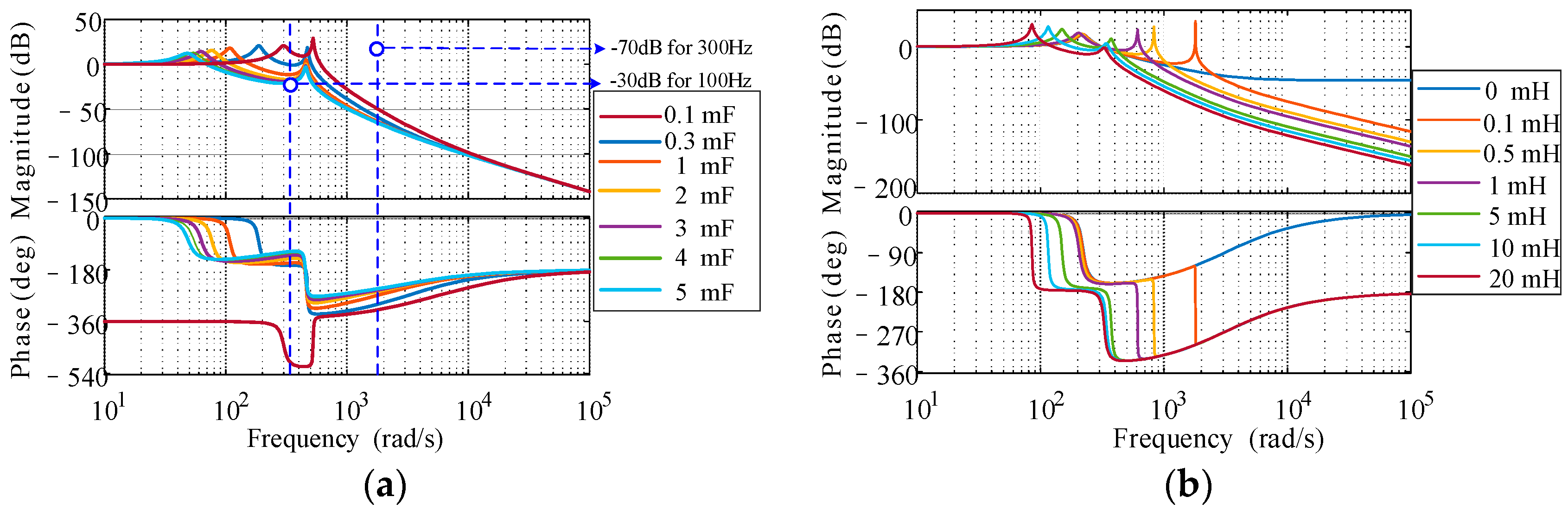
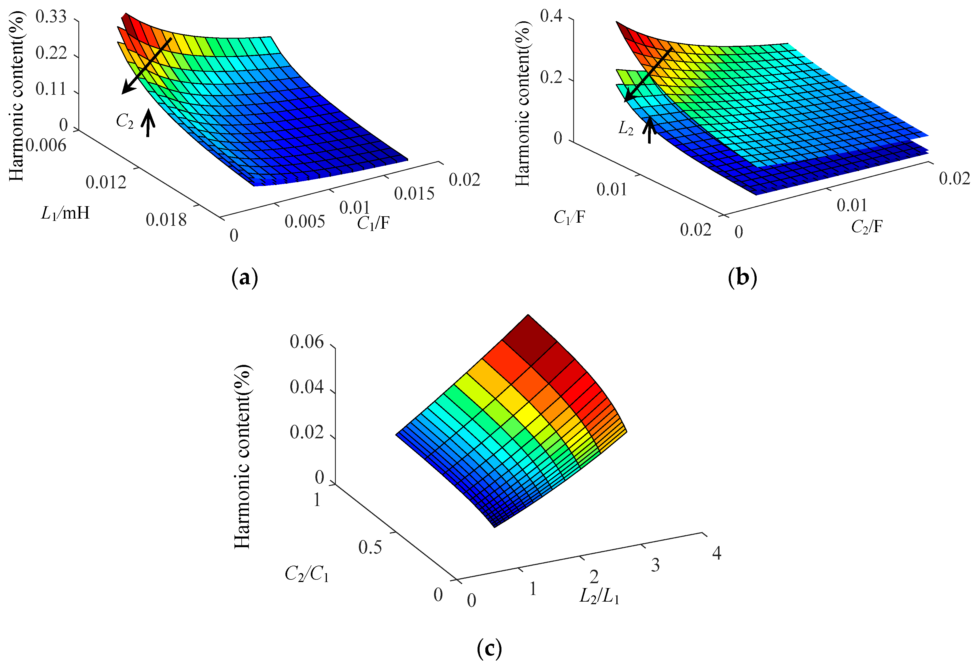
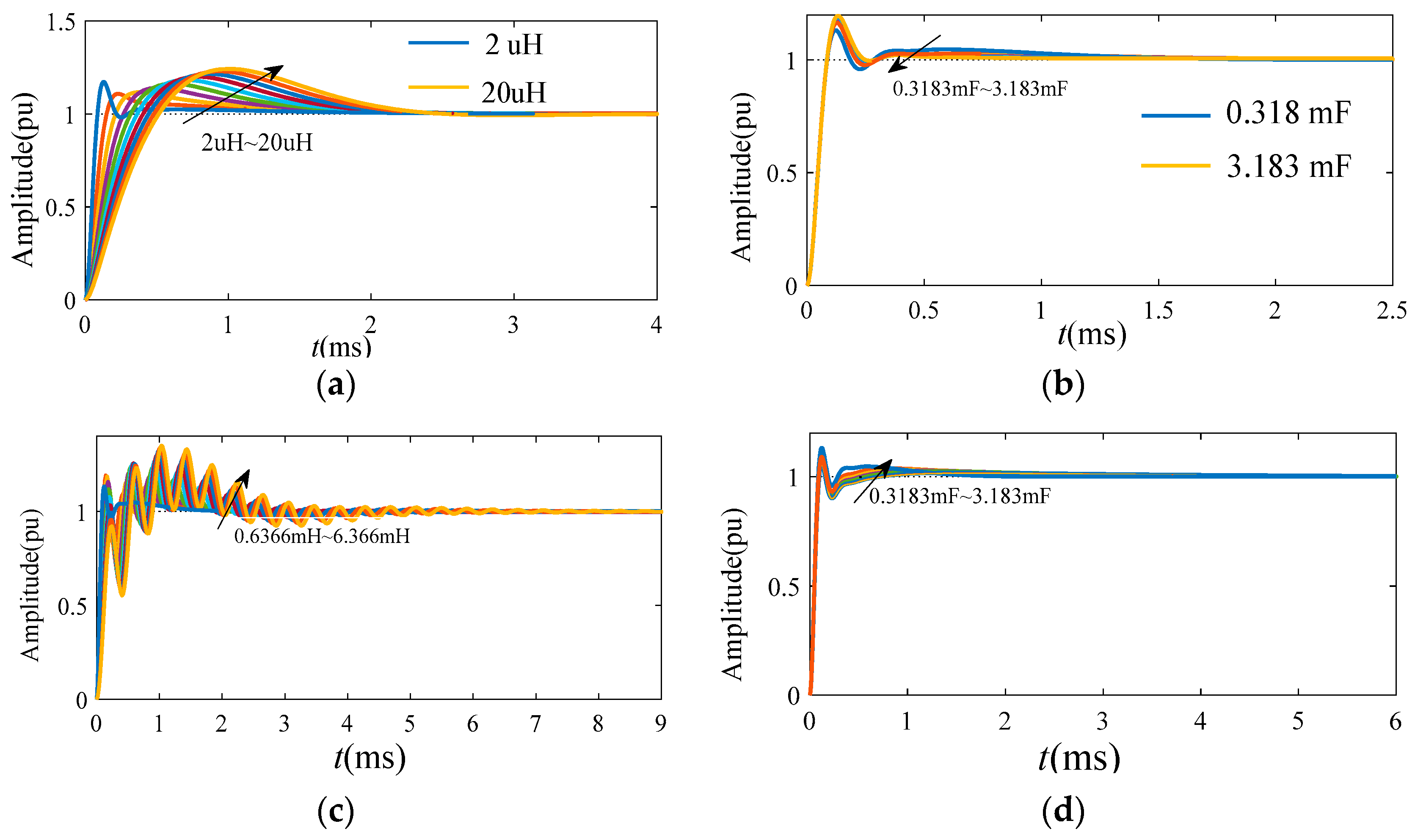
3.2. Sensitivity Analysis of Filter Parameters

The output admittance transfer function of the DC filter network was derived as expressed in Equation (17), which reflects the relationship between the output current and voltage. In Figure 8, the resonance peak value of the transfer function for the filter is minimal when the C1, C2, L1, and L2 branches contain resistance. However, when resistance emerges on the inductance branches, the output current has a certain attenuation effect on the output DC voltage. When the capacitance contained resistance, the output current attenuated the output DC voltage less than the inductance branch, and the resonance peak of the filter network was effectively diminished. Therefore, adding the damping components to the filter capacitance branch could accelerate the filter response time and slightly attenuate the DC voltage:
i o ( s ) U o ( s ) = s 3 C 1 C 2 ( L 1 R L 2 + L 1 R C 1 + L 1 R C 2 + L 2 R C 1 + L 2 R L 1 ) + s ( R L 1 C 2 + R L 2 C 2 + R C 2 C 2 + R C 1 C 1 + R L 1 C 1 ) + s 4 L 1 L 2 C 1 C 2 + s 2 [ C 1 C 2 ( R L 1 R L 2 + R C 1 R C 2 + R C 1 R L 2 + R C 1 R L 1 + R C 2 R L 1 ) + L 1 C 2 + L 2 C 2 + L 1 C 1 ] + 1 s 4 L 1 L 2 C 1 C 2 + s 3 [ C 1 C 2 ( R L 2 R C 2 L 1 + R C 1 R C 2 L 2 + R L 1 R C 2 L 2 + R C 1 R C 2 L 1 ) + L 1 L 2 C 1 ] + ( R L 1 + R L 2 ) s 2 [ C 1 ( R L 2 L 1 + R C 1 L 2 + R L 1 L 2 + R C 1 L 1 ) + C 1 C 2 ( R C 1 R C 2 R L 2 + R L 1 R L 2 R C 2 + R C 1 R C 2 R L 1 ) s [ C 1 ( R C 1 R L 2 + R L 1 R L 2 + R L 1 R C 1 ) + C 2 ( R L 1 R C 2 + R L 2 R C 2 ) + L 1 + L 2 ] + R C 2 C 2 ( L 1 + L 2 ) ]
The voltage transfer characteristics of the FRF and DFRF were obtained by substituting the parameters in Table 2 into Equation (13) and Table 3 into Equation (14), as demonstrated in Figure 9. In this figure, the resonant peak value at the resonant point significantly decreases, and the transfer speed of the filter theoretically accelerates when the capacitance branch is added to the resistor. Simultaneously, increasing damping resistance improves the high-frequency characteristics of the filter, thereby enlarging the slope of the high-frequency section.
The voltage transfer characteristic can be obtained by changing C1 from 0.1 mF to 5 mF, as exhibited in Figure 10a. In this figure, when the capacitance parameter was less than 1 mF (i.e., the ratio of C1 and C2 was greater than 3), the stopband attenuation characteristics of the filter were particularly poor, especially for low-frequency harmonics. When the ratio of C2 to C1 was smaller than 1, the stopband attenuation of the filter significantly improved. When the parameter of C1 was 5 mF, the harmonic attenuation of the filter for 100 Hz was −30 dB, and the attenuation for 300 Hz was 70 dB. The voltage transfer characteristics can be obtained by changing L1 from 0 mH to 20 mH, as displayed in Figure 10b. In this figure, if the inductance parameter is set to 0 mH, then the attenuation value of the filter to high-frequency harmonics finally approaches a constant, which is nonconducive to removing high-frequency harmonics. A large inductance parameter implies a large attenuation of the filter for the same frequency voltage harmonics. However, increasing L1 is bound to increase the response time of the filter simultaneously, and the design parameters should not increase the parameters of L1, as much as possible.
This study uses the second harmonic as an example for analyzing the relationship between the harmonic content and the parameters of the filter to accurately observe the attenuation of DC voltage harmonics. In Equation (13), S = j × 2π × 100 was set, which is the second harmonic content of the output voltage. In MATLAB, a three-dimensional (3D) diagram of the variation of the second harmonic content with C1 and L1 was drawn, as presented in Figure 11a. In this figure, under the same L2 and C2 parameters, a large L1 and C1 indicate a small second harmonic content. This result was consistent with the results of the previous analysis. When the parameters of C2 increased, the second harmonic content decreased. In practical applications, their parameters should be reasonably selected in accordance with the capacity of the DC distribution system. The relationship between the second harmonic content and the C1/C2 is illustrated in Figure 11b. Evidently, the second harmonic content decreased with increases in C1, C2, and L2.
Similarly, the relationship between the second harmonic content and the C2/C1 and L2/L1 was obtained, as depicted in Figure 11c. In this figure, small C2/C1 and L2/L1 denote a small content harmonic content. Moreover, C1 + C2 and L1 + L2 must satisfy certain conditions, and their value should be within a reasonable range. In addition, the response speed of the filter should be considered. Therefore, the values of L1, L2, C1, and C2 could not be too large because a small value is favorable when the filtering requirements are satisfied.

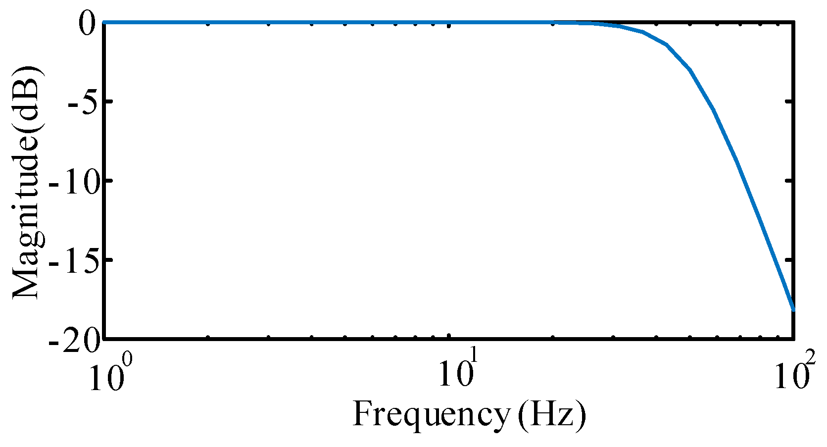
3.3. Dynamic Performance Analysis of the Filter
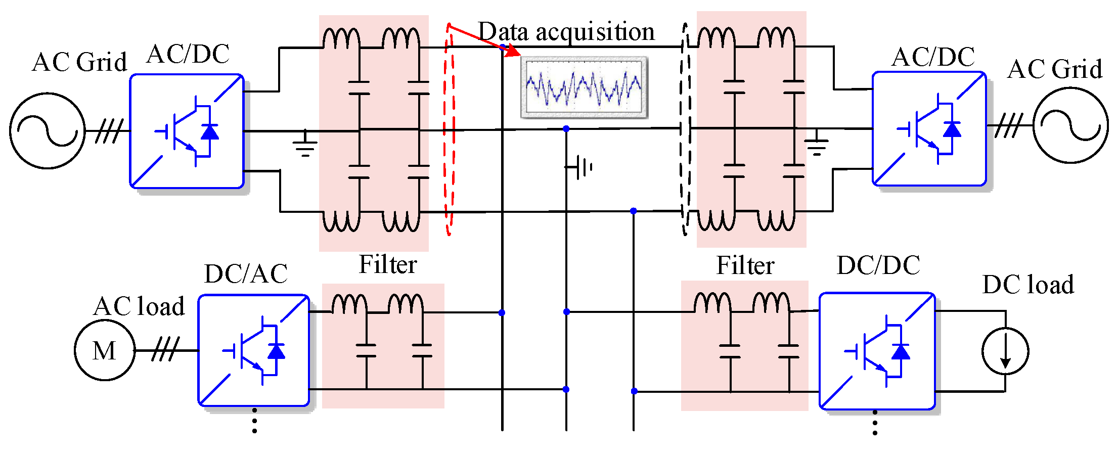
The root locus and Nyquist curves for the voltage transfer function of the filter were drawn in MATLAB using Equation (13), as demonstrated in Figure 12. In this figure, all closed-loop poles are located in the left-half plane, and Nyquist curves do not pass through (−1, j0), thus indicating that the filtering system is stable. The closed-loop poles of the voltage transfer function were close to the imaginary axis when the value of L1 changed from 2 mH to 20 mH. Based on the theory of control system, this approach extends the response time of the filter.
The step response of the filter was obtained by changing the parameters of the filter, as exhibited in Figure 6. Notably, only one component parameter was changed at a time, and changing the parameters of the filter should make the cut-off frequency of the filter only slightly different. The results are displayed in Figure 13. The response time of the filter and the overshoot increased with the increase of L1 from 2 mH to 20 mH, as presented in Figure 13a. In Figure 13b, C1 changes from 0.318 mF to 3.183 mF. In this figure, the change in C1 slightly affects the filter’s response time and overshoot. The inductance L2 changes from 0.6366 mH to 6.366 mH. The increase in L2 augmented the overshoot of the filter but only slightly affected the response time of the filter. In Figure 13d, the increase in C2 evidently augmented the response time of the filter, but the change in overshoot was particularly small.
Further analysis of the effect of the component parameters on the filter response time and overshoot is illustrated in Figure 14. In this figure, the filter response time, overshoot, and variation trend in different component parameters are presented.
The response time and overshoot of the filter were relatively small under the designed parameters of the filter, and the variation of the response time ranged from 0.2 to 1.2 ms. In addition, the overshoot did not exceed 0.4. Therefore, the designed parameters of the filter demonstrated a favorable dynamic performance and could resist the influence of the inaccuracy of parameters in practical engineering. According to the abovementioned analysis, C1 slightly affected the filter’s response time and overshoot, and its parameter selection is relatively flexible. The values of L1 and C2 significantly affected the filter’s response time, and the parameters of these two components should be increased in the design as little as possible. The increase in L2 would magnify the overshoot of the filter, thereby possibly negatively affecting the design.

4. Simulation Study

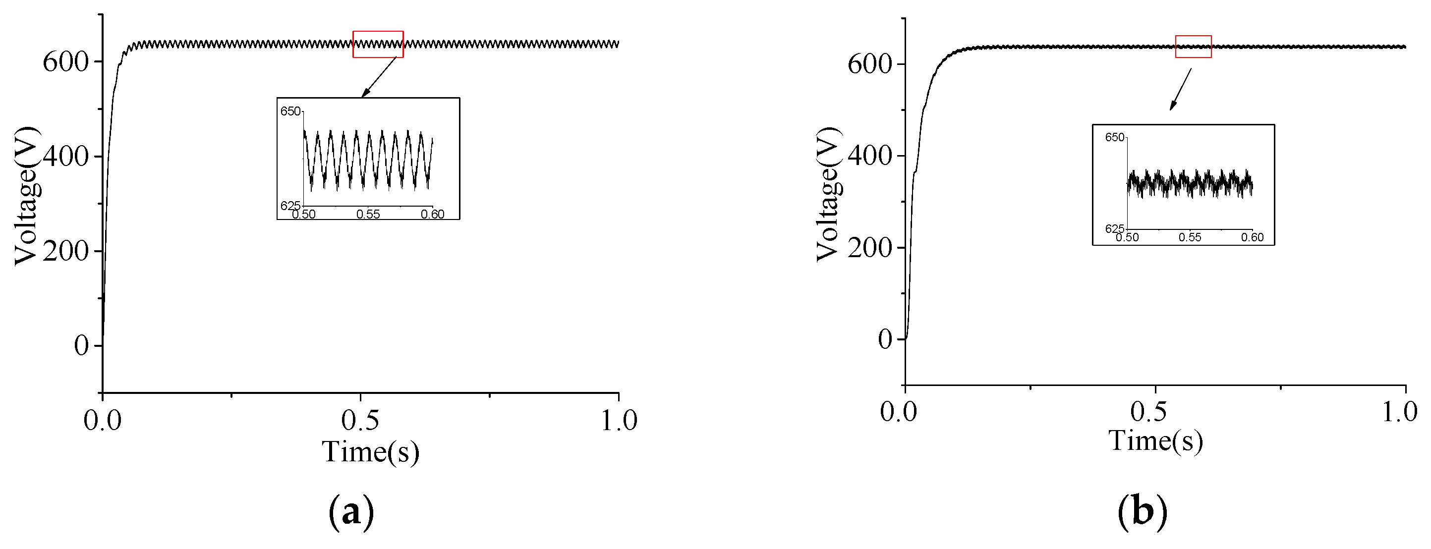
4.1. Simulation of Filtering Effect in Bipolar DC Distribution Networks

The bipolar DC distribution network, a common structure in the DC distribution network, can provide three voltage interfaces on the DC side to realize the flexible access of the DC load [11]. The FRF was used to create the DC filter network. The network structure and its basic parameters are exhibited in Figure 15 and Table 4, respectively. For the sake of simplicity, only one measurement point of the voltage waveform was set in the bipolar DC distribution network. The location of the measurement point is displayed in Figure 12.
The LCF and FRF were installed at the DC side. The LCF parameters were C = 4700 uF and L = 200 uH, and those of the FRF were the same as the data summarized in Table 1. The three-phase voltage unbalance factor on the AC side was 2%, and the simulation results of the DC bus voltage are presented in Figure 16.
The voltage fluctuation ranges of the LCF and FRF output waveforms were ±7.5 and ±3.5 V, respectively, indicating that the FRF slightly suppressed the DC voltage pulsation. The TF was installed on the DC side, and its simulation results are illustrated in Figure 17a,b. Evidently, the TF would generate a large resonance peak, thereby resulting in a rise in the filter response time. In addition, the filtering effect was poor, and the total harmonic distortion rate reached 4.8%. The parameters of the FRF listed in Table 1 were adopted to compare the filtering effects with the DNMFRF. The parameters of the DNMFRF are listed in Table 3, and the simulation results are demonstrated in Figure 17c,d. Evidently, the ability of the FRF in suppressing the resonance peak and accelerating the transfer speed of the filter was worse than the DNMFRF.

4.2. Simulation Result of Single-Ended Radial DC Distribution Networks

The single-ended radial DC distribution network developed in the present study was connected to an AC network through a six-pulse rectifier. The DC side was connected to the AC and DC loads, and photovoltaics through DC/AC or DC/DC converters. The basic structure and parameters of the network are displayed in Figure 18 and Table 5, respectively. The characteristic harmonics on the DC side were 6k (k = 1, 2, 3, …, n) order and contained the modulated harmonics of switching frequency whose frequency was N + 1 (N = 0, 1, 2, …, n) times of the switching frequency.
As shown in Figure 19a,b, the TF had a poor filtering effect in this model. The total harmonic distortion rate of the output voltage on the DC side reached 5.14%. When the three-phase unbalance factor of the AC voltage was 2%, the filtering effect of the FRF and LCF were compared. The total harmonic distortion rate of the output voltage of the LCF reached 1.15% (Figure 19c,d), whereas the rate was 0.28% for FRF and DNMFRF (Figure 19e,f). The results showed that the FRF demonstrates an improved effect in suppressing the low-frequency pulsation caused by three-phase unbalance compared to the LCF. Moreover, when the DNMFRF was installed in the DC-side of the DC distribution network, it had the same filtering effects as the FRF and could restrict the resonance peak value, accelerate the transfer speed, and maintain the steady filtering result.
Resistance was added to the inductance branch, and the simulation results for various cases are presented in Figure 20a. In this figure, the filter had the shortest response time when the capacitance and inductance branches contained damping resistances. However, the damping resistance in the inductance branch had a certain attenuation for the DC voltage, whereas the resistance in the capacitance branch had a small attenuation on the DC voltage. The load type of the DC distribution network was changed, and the situation in which the DC distribution network contains 100% and 50% constant-power and constant-resistive loads. The simulation results are illustrated in Figure 20b. In this figure, when all the loads in the DC distribution network were constant-resistive load, the DC voltage had the smallest resonance peak and fastest response time. When the load of the DC distribution network was all constant-power load, the situation was the opposite. Evidently, the filtering effect of the filter is also related to the type of DC load, and the constant-power load requires high filtering performance.

4.3. Simulation of the Power Transmission Efficiency in Single-Ended Radial DC Distribution Network

The fluctuation magnitude of the DC bus current affects the voltage drop on the smoothing reactor and the DC transmission line. Evidently, the straight voltage waveform affects the power transmission efficiency of the DC distribution network. Based on the simulation filtering results in the single-ended radial DC distribution network, the voltage across the smoothing reactor was analyzed using FFT. The DC component of the voltage drop waveform on the smoothing reactor using DNMFRF is depicted in Figure 21a, where in the DC component was approximately 1 V, whereas that on the LCF was approximately 3 V, as demonstrated in Figure 21b. Accordingly, the DNMFRF filter reduced the transmission voltage loss.
The load frequently changed in the DC distribution network, which promoted the current in the DC transmission line to change regularly. The load was changed in the single-ended distribution simulation model to further analyze the power transmission efficiency of the filter. The input and output powers of the rectifier and inverter, respectively, were measured to compare the transmission efficiency of the DNMFRF and LCF. The transmission efficiency was defined as the ratio of the total output power of the inverter to the total input power of the rectifier. The results are exhibited in Figure 22. In this figure, the power transmission efficiency was worse in the LCF than in the DNMFRF in the DC distribution network. When the load changed, the transmission efficiency of the designed filter was minimally affected by the load fluctuation.

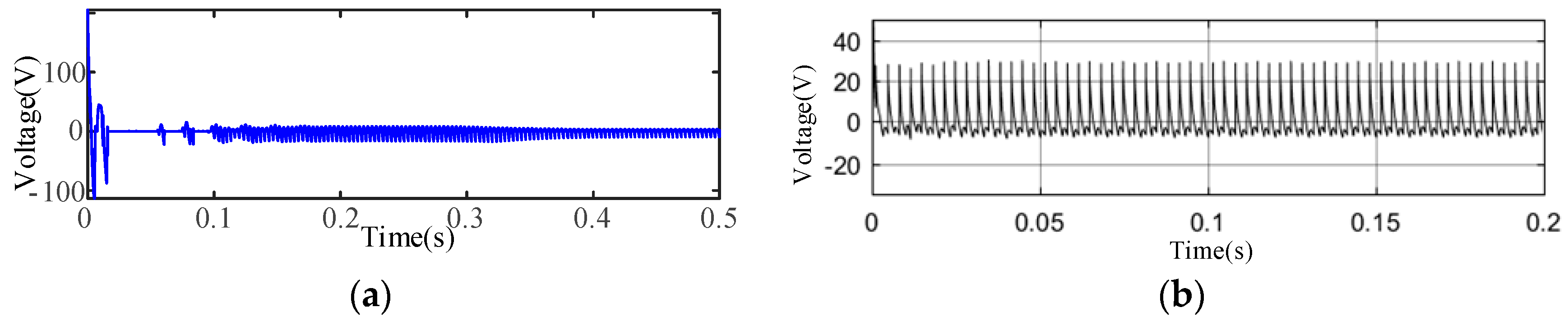
5. Experimental Study

An experimental platform for a single-ended radial DC distribution network was created to further verify the advantages of FRF in improving the DC voltage quality in the DC distribution network, as displayed in Figure 23. The parameters of the test platform were as follows: Chroma 61845 Programmable AC power source (Chroma Systems Solutions, Inc., Foothill Ranch, CA, USA) was used to supply the DC power. The effective voltage value of the AC line was set to 20 V, and two groups of adjustable DC loads were supplied by the six-pulse rectifier bridge. The initial trigger angle of the 6-pulse rectifier bridge was 15°, and the rated voltage on the DC side was 45 V. The original current was 4 A. Furthermore, the smoothing reactor took 2 mH, and a resistance of 0.1 Ω was replaced by two copper bars. A total of 2500 points on the waveform before filtering, and those of LCF and FRF, were programmed by MATLAB to obtain the Fourier analysis results of the three groups of data. The obtained waveforms are presented in Figure 24a–d. The experimental results show that the total harmonic distortion rate is 5.63% before filtering, and 2.6% and 0.59% for LCF and FRF, respectively).
The power supply voltage of programmable AC power supply was changed to 600 V to obtain a 500 V DC voltage from the DC side, and the number of DC loads was simultaneously increased to 4. The total current of the DC bus was 20 A. The DC voltage of the LC filter and FRF were installed at the DC side, which waited until the stage of Loads 1 and 2, as shown in the figure. The power of the DC load (the DC bus current for light and heavy loads were 10 and 30 A, respectively) was changed, and the voltage of each node was measured. The experimental results are illustrated in Figure 25. In this figure, the DC voltage attenuation using FRF filtering was small under a heavy load because the ripple in the DC current had a voltage drop when smoothing the reactor and DC transmission line. Moreover, the DC voltage attenuation was small for the FRF case because the FRF inhibited the DC ripple to a small degree.

6. Conclusions

In this study, a low-ripple and fast-response filter was designed to improve the DC voltage quality of a DC distribution network, called DNMFRF. Simulations and experimental results confirmed that the filter has a low resonance value, rapid conversion ability, and excellent filtering effect. The designed filter can diminish the loss of smoothing reactor and DC transmission line during the transmission of DC voltage over TF and LCF, indicating its high power transmission efficiency. The parameter optimization method based on the pole-circle restricts the resonant peak value of the resonant point and accelerates the transfer speed of the filter. From the perspectives of investment cost, occupational area, filtering effect, and response speed, the filter designed in this study can improve the voltage quality in a DC distribution network compared to other filters, thereby verifying the suitability of the designed filter for DC-side filtering of DC distribution networks.

Author Contributions

N.Z. and J.L. proposed the idea of using DNMFRF to mitigate the low-frequency pulsation; J.L. derived the equations. Q.W. built the simulation model and analyzed the data. All authors were involved in preparing the manuscript.

Acknowledgments

This research was funded by [National Natural Science Foundation of China] grant number [51877017] and [National key research and development program] grant number [2018YFB0904604].

Conflicts of Interest

The authors declare no conflict of interest.

References

  1. Deng, W.; Pei, W.; Li, L.Y. Active Stabilization Control of Multi-Terminal AC/DC Hybrid System Based on Flexible Low-Voltage DC Power Distribution. Energies 2018, 11, 502. [Google Scholar] [CrossRef]
  2. Kim, J.H.; Kim, J.Y.; Cho, J.T.; Song, I.K.; Kweon, B.M.; Chung, I.Y.; Choi, J.H. Comparison between Underground Cable and Overhead Line for a Low-Voltage Direct Current Distribution Network Serving Communication Repeater. Energies 2014, 7, 1656–1672. [Google Scholar] [CrossRef] [Green Version]
  3. Wang, M.H.; Tan, S.C.; Lee, C.K.; Hui, S.Y.R. A Configuration of Storage System for DC Microgrids. IEEE Trans. Power Electron. 2017, 33, 3722–3733. [Google Scholar] [CrossRef]
  4. Chen, X.; Shi, M.; Sun, H.; Li, Y.; He, H. Distributed Cooperative Control and Stability Analysis of Multiple DC Electric Springs in a DC Microgrid. IEEE Trans. Ind. Electron. 2018, 65, 5611–5622. [Google Scholar] [CrossRef]
  5. Liu, Y.; Hou, X.C.; Wang, X.F.; Lin, C.; Guerrero, J.M. A Coordinated Control for Photovoltaic Generators and Energy Storages in Low-Voltage AC/DC Hybrid Microgrids under Islanded Mode. Energies 2016, 9, 651. [Google Scholar] [CrossRef]
  6. Van der Blij, N.H.; Ramirez-Elizondo, L.M.; Spaan, M.T.J.; Bauer, P. Stability of DC Distribution Systems: An Algebraic Derivation. Energies 2017, 10, 1412. [Google Scholar] [CrossRef]
  7. Kakigano, H.; Miura, Y.; Ise, T. Low-Voltage Bipolar-Type DC Microgrid for Super High Quality Distribution. IEEE Trans. Power Electron. 2010, 25, 3066–3075. [Google Scholar] [CrossRef]
  8. Wang, M.H.; Mok, K.T.; Tan, S.C.; Hui, S.Y.R. Multifunctional DC Electric Springs for Improving Voltage Quality of DC Grids. IEEE Trans. Smart Grid 2018, 9, 2248–2258. [Google Scholar] [CrossRef]
  9. Mok, K.T.; Wang, M.H.; Tan, S.C.; Hui, S.Y.R. DC Electric Springs—A Technology for Stabilizing DC Power Distribution Systems. IEEE Trans. Power Electron. 2016, 32, 1088–1105. [Google Scholar] [CrossRef]
  10. Sahoo, S.; Prakash, S.; Mishra, S. Power Quality Improvement of Grid Connected DC Microgrids using Repetitive Learning Based PLL under Abnormal Grid Conditions. IEEE Trans. Ind. Appl. 2017, 54, 82–90. [Google Scholar] [CrossRef]
  11. Wang, H.; Blaabjerg, F. Reliability of Capacitors for DC-Link Applications in Power Electronic Converters—An Overview. Ind. Appl. IEEE Trans. 2014, 50, 3569–3578. [Google Scholar] [CrossRef]
  12. Gu, L.; Ruan, X.; Xu, M.; Yao, K. Means of Eliminating Electrolytic Capacitor in AC/DC Power Supplies for LED Lightings. IEEE Trans. Power Electron. 2009, 24, 1399–1408. [Google Scholar] [CrossRef]
  13. Lehman, B.; Wilkins, A.; Berman, S.; Poplawski, M.; Miller, N.J. Proposing Measures of Flicker in the Low Frequencies for Lighting Applications. LEUKOS 2011, 7, 189–195. [Google Scholar]
  14. Shimizu, T.; Jin, Y.; Kimura, G. DC ripple current reduction on a single-phase PWM voltage-source rectifier. IEEE Trans. Ind. Appl. 2000, 36, 1419–1429. [Google Scholar] [CrossRef]
  15. Krein, P.T.; Balog, R.S.; Mirjafari, M. Minimum Energy and Capacitance Requirements for Single-Phase Inverters and Rectifiers Using a Ripple Port. IEEE Trans. Power Electron. 2012, 27, 4690–4698. [Google Scholar] [CrossRef]
  16. Jung, T.H.; Gwon, G.H.; Kim, C.H.; Han, J.; Oh, Y.S.; Noh, C.H. Voltage Regulation Method for Voltage Drop Compensation and Unbalance Reduction in Bipolar Low-Voltage DC Distribution System. IEEE Trans. Power Deliv. 2018, 33, 141–149. [Google Scholar] [CrossRef]
  17. Graham, A.D. The Importance of A DC Side Harmonic Study for A DC Distribution System. In Proceedings of the IET International Conference on Power Electronics, Machines and Drives, Bristol, UK, 27–29 March 2012; pp. 1–5. [Google Scholar]
  18. Hu, Y.; Du, Y.; Xiao, W.; Finney, S.; Cao, W. DC-link voltage control strategy for reducing capacitance and total harmonic distortion in single-phase grid-connected photovoltaic inverters. IET Power Electron. 2015, 8, 1386–1393. [Google Scholar] [CrossRef]
  19. Li, S.; Lee, A.T.L.; Tan, S.C.; Hui, S.Y. Plug-and-Play Voltage Ripple Mitigator for DC Links in Hybrid AC-DC Power Grids with Local Bus-Voltage Control. IEEE Trans. Ind. Electron. 2017, 65, 687–698. [Google Scholar] [CrossRef]
  20. Wang, M.H.; Yan, S.; Tan, S.C.; Hui, S.Y. Hybrid-DC Electric Springs for DC Voltage Regulation and Harmonic Cancellation in DC Microgrids. IEEE Trans. Power Electron. 2018, 33, 1167–1177. [Google Scholar] [CrossRef] [Green Version]
  21. Lee, T.L.; Wang, Y.C.; Li, J.C.; Guerrero, J.M. Hybrid Active Filter with Variable Conductance for Harmonic Resonance Suppression in Industrial Power Systems. Ind. Electron. IEEE Trans. 2015, 62, 746–756. [Google Scholar] [CrossRef]
  22. Somlal, J.; Rao, M.V.G. Power conditioning in distribution systems using ANN controlled Shunt Hybrid Active Power Filter. In Proceedings of the International Conference on Smart Electric Grid, Guntur, India, 19–20 September 2014. [Google Scholar]
  23. Wang, Z.; Wu, B.; Xu, D.; Cheng, M.; Xu, L. DC-Link Current Ripple Mitigation for Current-Source Grid-Connected Converters Under Unbalanced Grid Conditions. IEEE Trans. Ind. Electron. 2016, 63, 4967–4977. [Google Scholar] [CrossRef]
  24. Li, H.; Zhang, L.; Yan, X.; Kang, W. Design Method of Low Loss and Fast Response LC Filters Based on Locomotive Battery Testing System. EPE J. 2008, 18, 25–31. [Google Scholar]
  25. Beres, R.N.; Wang, X.; Liserre, M.; Blaabjerg, F.; Bak, C.L. A Review of Passive Power Filters for Three-Phase Grid-Connected Voltage-Source Converters. IEEE J. Emerg. Sel. Top. Power Electron. 2017, 4, 54–69. [Google Scholar] [CrossRef]
  26. Yang, L.; Chen, Y.; Luo, A.; Wu, W.; Huai, K.; Zhou, X.; Zhou, L.; Xu, Q.; Guerrero, J.M. Second Ripple Current Suppression by Two Band-Pass Filters and Current Sharing Method for Energy Storage Converters in DC Microgrid. IEEE J. Emerg. Sel. Top. Power Electron. 2017, 5, 1031–1044. [Google Scholar] [CrossRef]
  27. Bo, C.; Zeng, X.; Yao, X. Three Tuned Passive Filter to Improve Power Quality. In Proceedings of the International Conference on Power System Technology, Chongqing, China, 22–26 October 2006. [Google Scholar]
  28. Fadloullah, I.; Mechaqrane, A.; Ahaitouf, A. Butterworth Low Pass filter design using evolutionary algorithm. In Proceedings of the International Conference on Wireless Technologies, Embedded and Intelligent Systems, Fez, Morocco, 19–20 April 2017; pp. 1–6. [Google Scholar]
  29. Kang, W.; Zhang, L.; Liu, C. Output filter design method in current-source PWM converters. Trans. China Electrotech. Soc. 2012, 27, 83–89. [Google Scholar]
  30. Aleem, S.H.E.A.; Balci, M.E.; Zobaa, A.F.; Sakar, S. Optimal passive filter design for effective utilization of cables and transformers under non-sinusoidal conditions. In Proceedings of the 16th International Conference on Harmonics and Quality of Power (ICHQP). Bucharest, Romania, 25–28 May 2014; pp. 626–630. [Google Scholar]
  31. Yang, N.C.; Le, M.D. Optimal Design of Passive Power Filters Based on Multi-Objective Bat Algorithm and Pareto Front; Elsevier: Amsterdam, The Netherlands, 2015; pp. 257–266. [Google Scholar]
  32. Sakar, S.; Balci, M.E.; Aleem, S.H.E.A.; Zobaa, A.F. Hosting capacity assessment and improvement for photovoltaic-based distributed generation in distorted distribution networks. In Proceedings of the IEEE International Conference on Environment and Electrical Engineering, Florence, Italy, 7–10 June 2016. [Google Scholar]
  33. Ali, Z.M.; Alenezi, F.Q.; Kandil, S.S.; Aleem, S.H.E.A. Practical considerations for reactive power sharing approaches among multiple-arm passive filters in non-sinusoidal power systems. Int. J. Electr. Power Energy Syst. 2018, 103, 660–675. [Google Scholar] [CrossRef]
  34. Zhang, L.; Gui, J.; Xing, C.; He, Z.; Zhan, G. Research on how to enhance the Chebyshev DC/DC filter’s performance. Phys. Procedia 2012, 24, 891–899. [Google Scholar]
  35. Zhang, L.; Xiangwu, Y.; Li, H.; Wei, K. Design and Simulation of Fast-Response Filter Based on Locomotive Battery Testing System. In Proceedings of the Power Electronics and Motion Control Conference, Portoroz, Slovenia, 30 August–1 September 2006. [Google Scholar]
Figure 1. Basic structure of a DC filter: (a) Double-tuned high-pass filter, (b) C-type filter, (c) Six-order damping-CBSF, and (e,f,g) APF.
Energies 11 03128 g001
Figure 2. Comparison of different passive filters: (a) LCF, FRF, CBSF; (b) TF; (c) Harmonic content for FRF and CBSF, and (d) Response time for FRF and CBSF.
Energies 11 03128 g002
Figure 3. DC distribution network diagram containing FRF.
Energies 11 03128 g003
Figure 4. Relationship between the attenuation characteristics and the order of the filter.
Energies 11 03128 g004
Figure 5. Attenuation characteristics of the third-order FRF.
Energies 11 03128 g005
Figure 6. DC filter structure of the FRF.
Energies 11 03128 g006
Figure 7. Zero-pole distribution and offset analysis of the FRF.
Energies 11 03128 g007
Figure 8. Frequency response characteristics of output admittance in DC filter networks.
Energies 11 03128 g008
Figure 9. Comparison of voltage transmission characteristics under different filters.
Energies 11 03128 g009
Figure 10. Effect of filter parameters on voltage transfer characteristics: (a) C1 change and (b) L1 change.
Energies 11 03128 g010
Figure 11. Relationship between the second harmonic content and parameters of the filter: (a) C1 and L1; (b) C1 and C2, and (c) C1/C2 and L2/L1.
Energies 11 03128 g011
Figure 12. (a) Root locus and (b) Nyquist curves of the voltage transfer function.
Energies 11 03128 g012
Figure 13. Step response of the filter under different parameters: (a) L1; (b) C1; (c) L2, and (d) C2.
Energies 11 03128 g013
Figure 14. (a) Response time and (b) overshoot of the filter under different component parameters.
Energies 11 03128 g014
Figure 15. Schematic of a double-ended distribution model.
Energies 11 03128 g015
Figure 16. Simulation results for different filters: (a) LCF and (b) FRF.
Energies 11 03128 g016
Figure 17. Simulation results for different filters: (a) Filtering waveform of TF; (b) Voltage spectrum of TF; (c) Filtering waveforms of DNMFRF and FRF, and (d) Voltage spectrum of DNMFRF and FRF.
Energies 11 03128 g017
Figure 18. Simulation model of the single-ended radial DC distribution network.
Energies 11 03128 g018
Figure 19. Comparison of the filtering performances for different filters. (a,b) TF; (c,d) FRF; (e,f) DNMFRF.
Energies 11 03128 g019
Figure 20. Comparison of the filtering performance for different cases. (a) Damping resistance is located in different branches of the filter and (b) Various types of DC loads.
Energies 11 03128 g020
Figure 21. Voltage drop on the smoothing reactor: (a) DNMFRF and (b) LCF.
Energies 11 03128 g021
Figure 22. Comparison of power transmission characteristics of two kinds of filters.
Energies 11 03128 g022
Figure 23. Experimental platform diagram.
Energies 11 03128 g023
Figure 24. Filtering experiment results: (a,b) LCF and (c,d) FRF.
Energies 11 03128 g024
Figure 25. Filtering experiment results for high-power applications. (a) FRF; (b) LCF, and (c) The voltage of each node under different loads.
Energies 11 03128 g025
Table 1. Characteristic comparison of different filters.
TypeApplicationAdvantageDisadvantage
APFAC or DC filteringDynamic compensation of harmonicsHigh cost, complex design and control
TFAC or DC filteringSimple principle and design methodLarge occupation area
LCFAC or DC filteringFew elements and low costLarge volume and small power density
FRFDC filteringFast response speedSlow stopband attenuation
CBSFDC filteringFast attenuation of stopbandSlow response speed
Table 2. Parameters value of filter elements.
ElementkmValue
C113.183 mF
L1-20 mH
C213.183 mF
L226.366 mH
Table 3. Optimized filter elements parameter value.
ElementkmValue
C11.484.7 mF
L1-2 mH
C213.183 mF
L226.366 mH
R1-0.1 Ω
R2-0.1 Ω
Table 4. Parameters of the bipolar double-ended DC distribution model.
ParameterValueParameterValue
Three-phase voltage unbalance factor (%)0–2%DC line resistance (Ω)0.2
AC voltage (V)220DC bus current (A)20
DC bus voltage (V)640DC load power (kW)1 × 10
Modulation ratio (pu)0.7AC load power (kW)2 × 1.4
Table 5. Parameter of the single-ended radial DC distribution network.
ParameterValueParameterValue
AC Voltage (V)220AC Load Power (kW)8 × 1
DC Bus Voltage (V)500DC Load Power (kW)8 × 1
Trigger Angle (°)10Switching Frequency (Hz)1000
DC Line Resistance (Ω)0.1DC Current (A)20

