Suppression of Switching Crosstalk and Voltage Oscillations in a SiC MOSFET Based Half-Bridge Converter


Abstract
1. Introduction
2. Gate Driver for SiC MOSFET
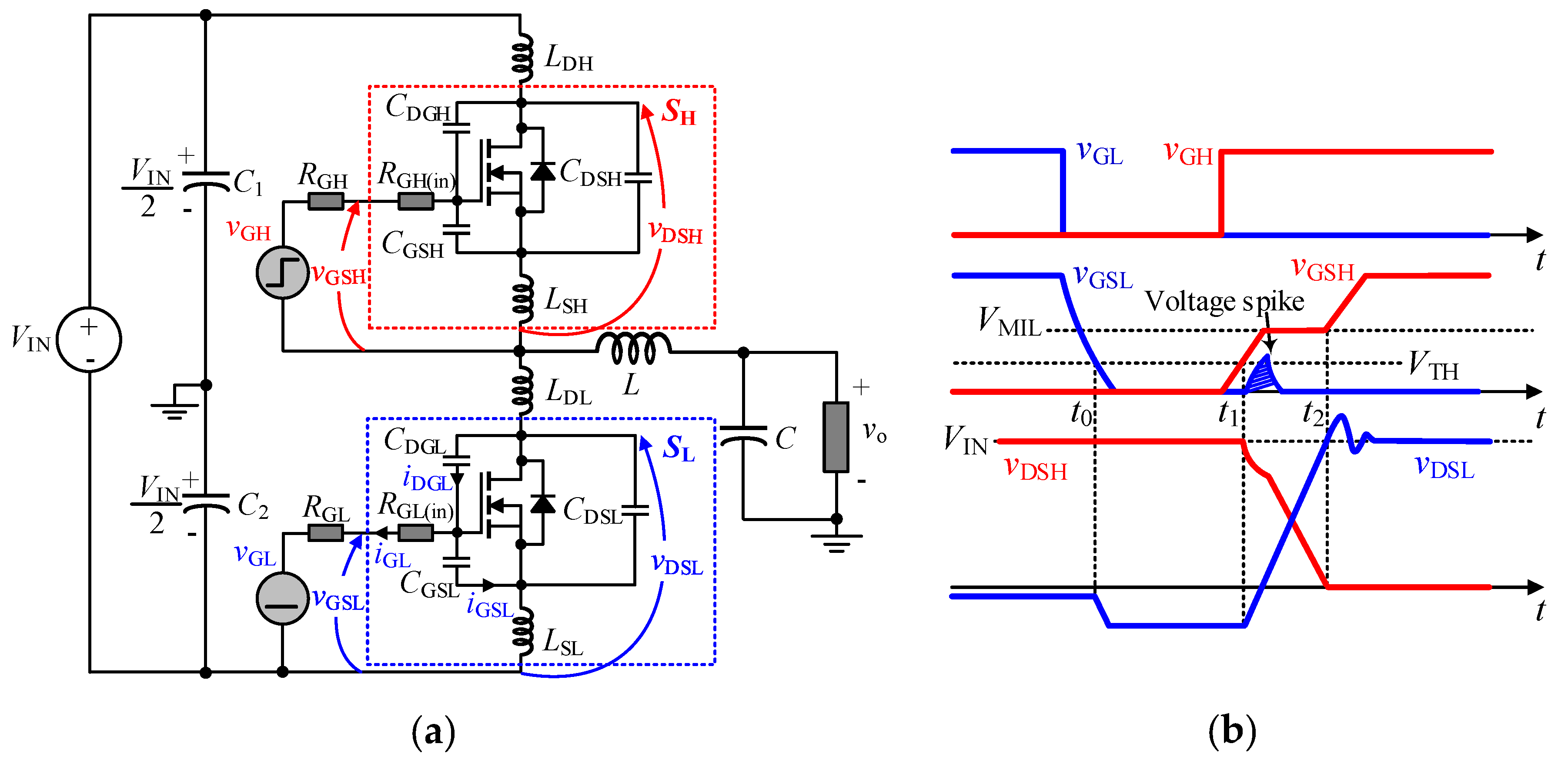
2.1. Crosstalk Phenomenon in Half-Bridge dc-ac Converter
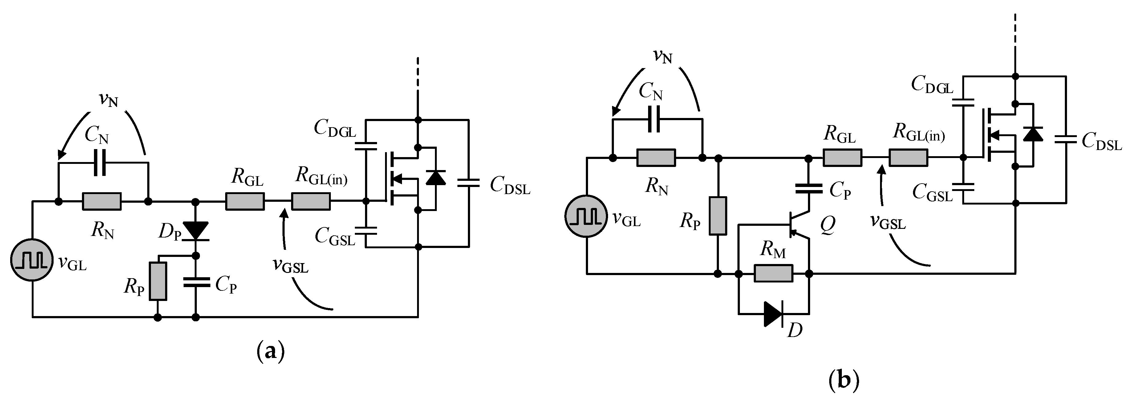
2.2. Previous Work on Gate Driver for SiC MOSFET with Level Shifter
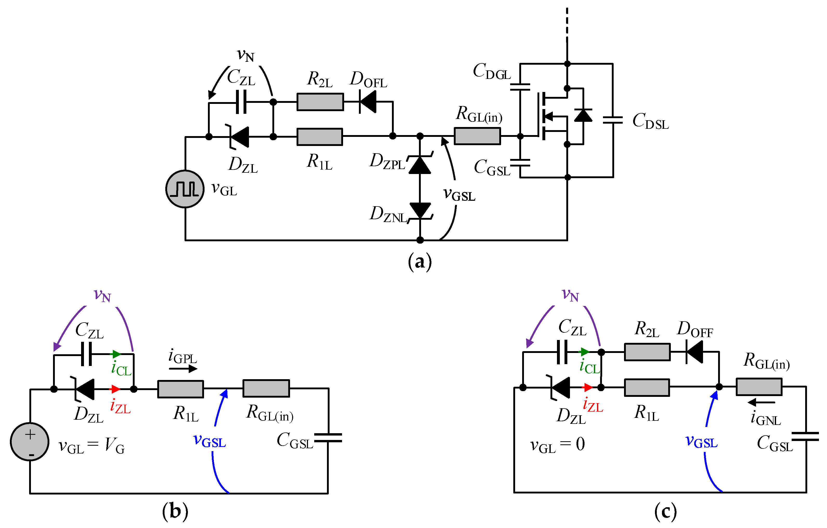
2.3. Proposed Gate Driver for SiC MOSFET
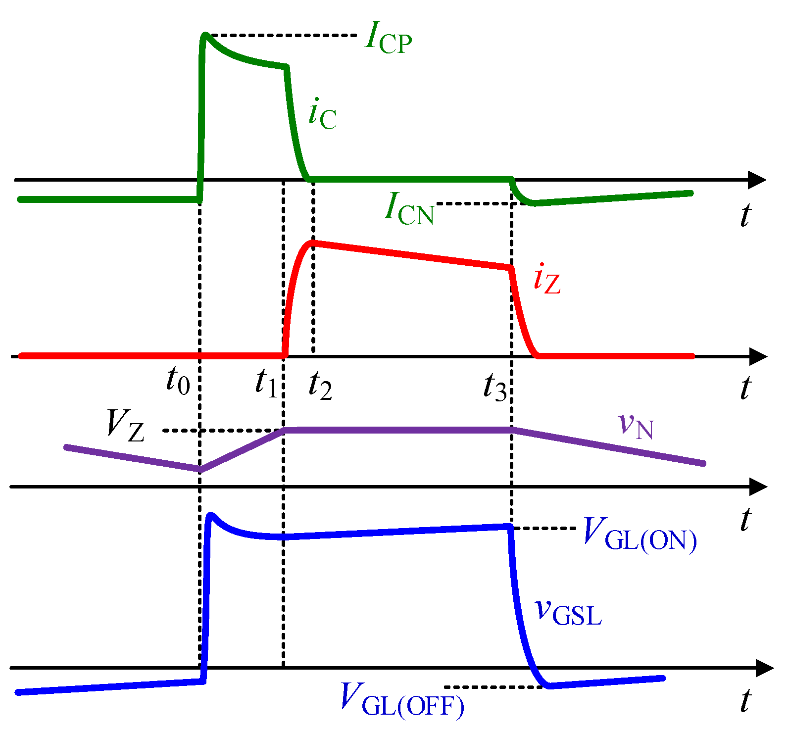
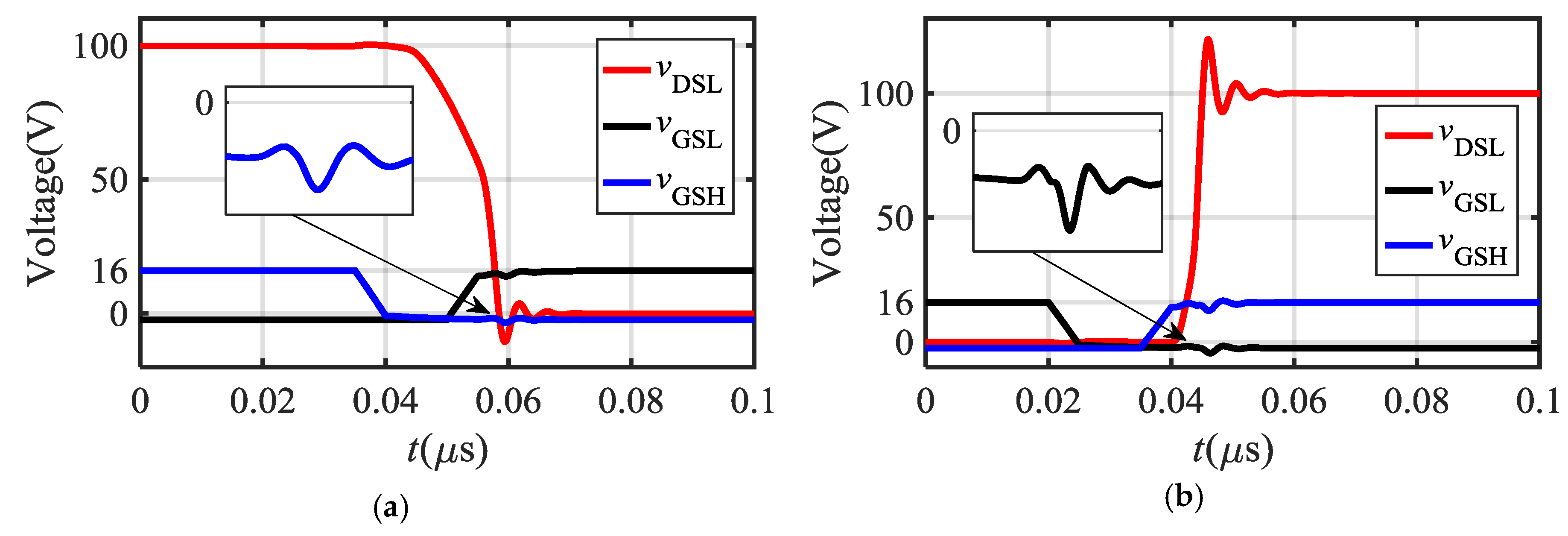
2.3.1. Turn-on Process
2.3.2. Turn-off Process
3. Effect of Parasitic Inductances on Switching Waveform of SiC MOSFET
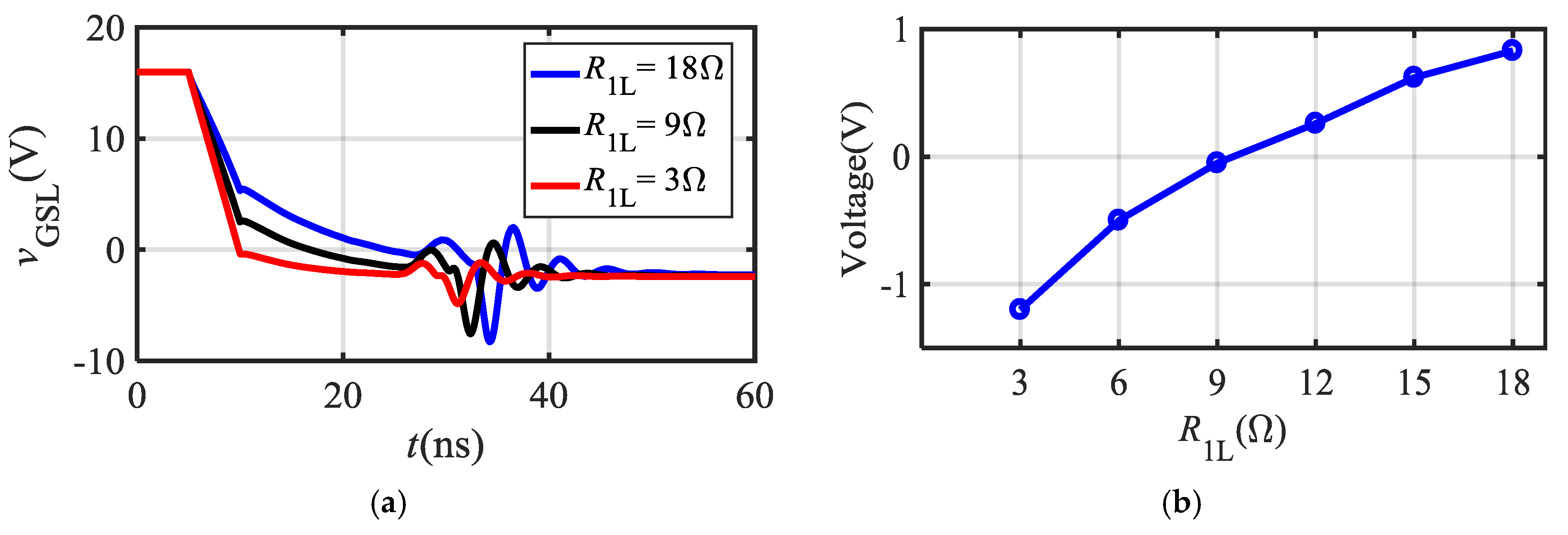
3.1. Overlap Conduction
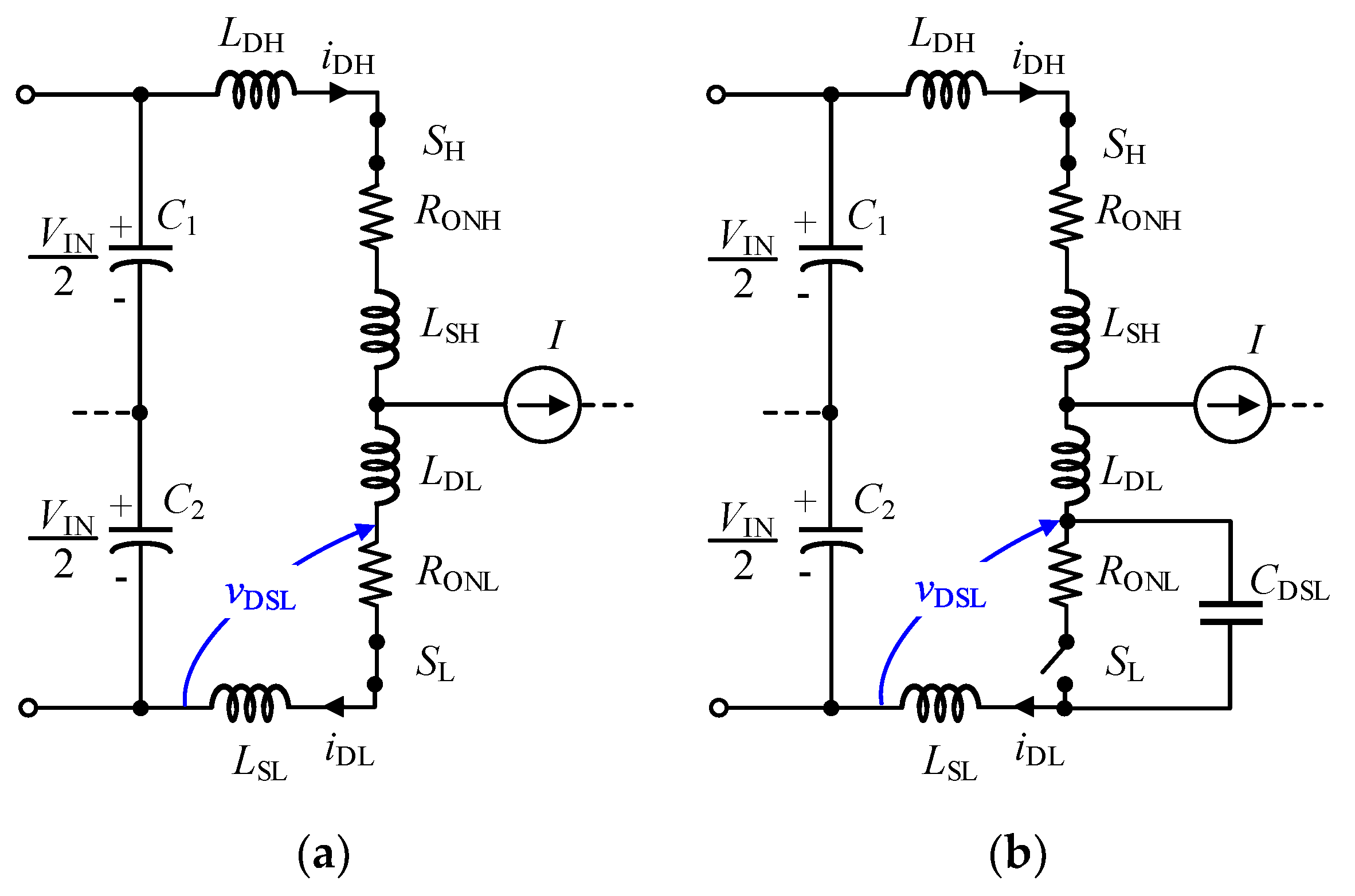
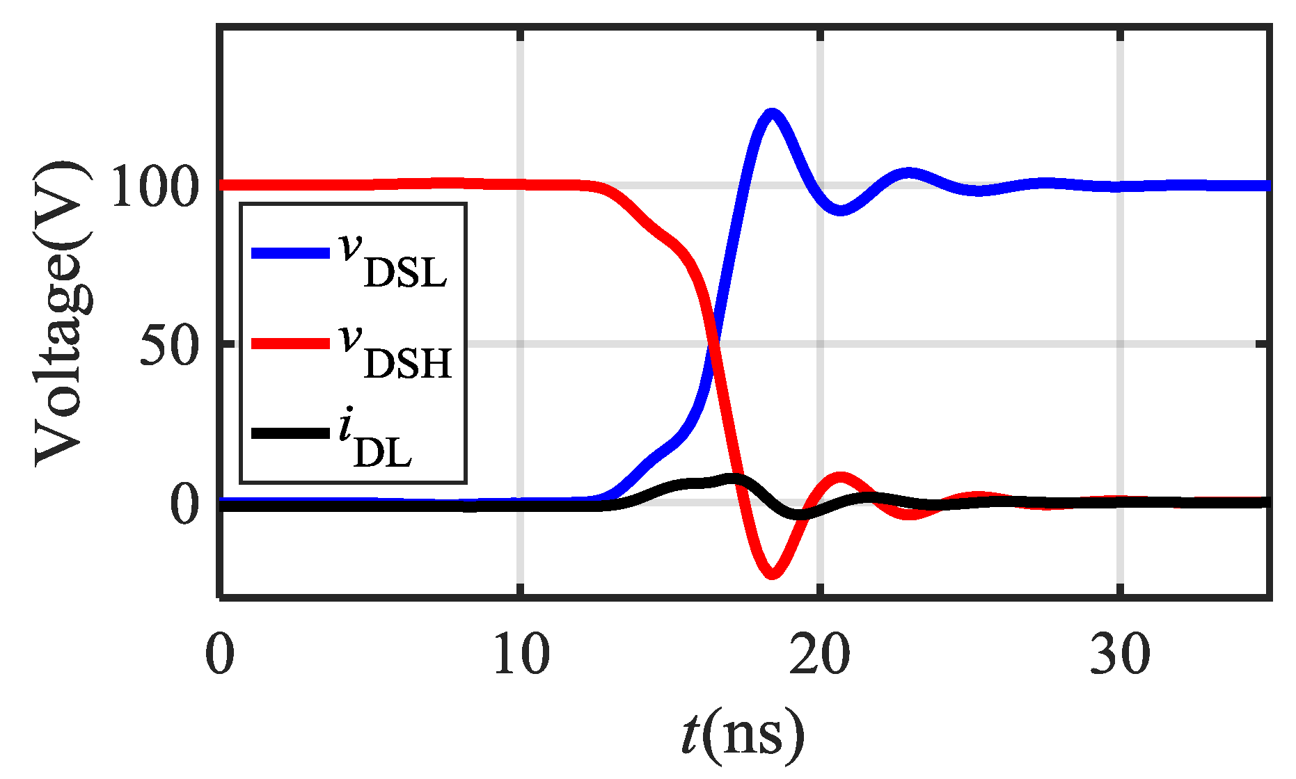
3.2. The SL Turn-off Transient
3.3. PCB Guidelines
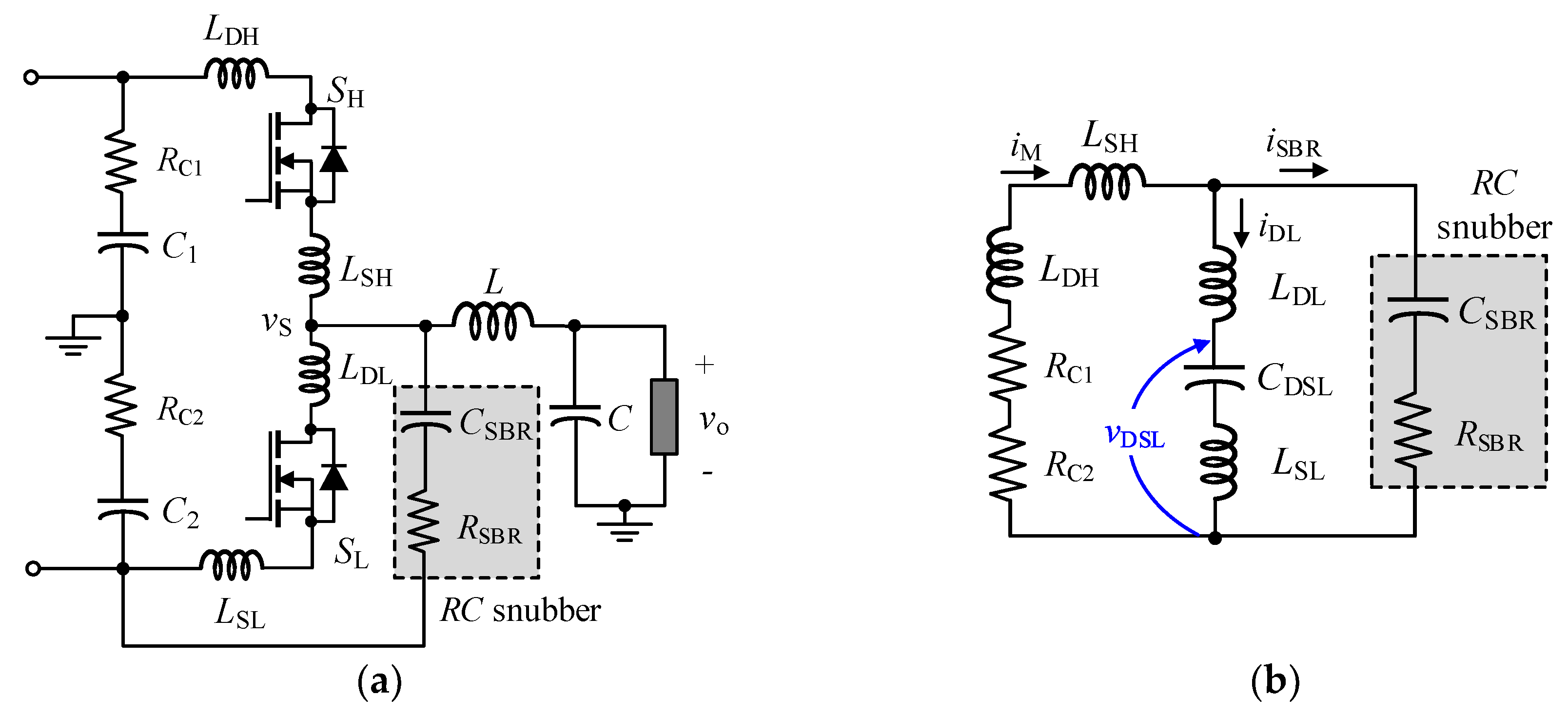
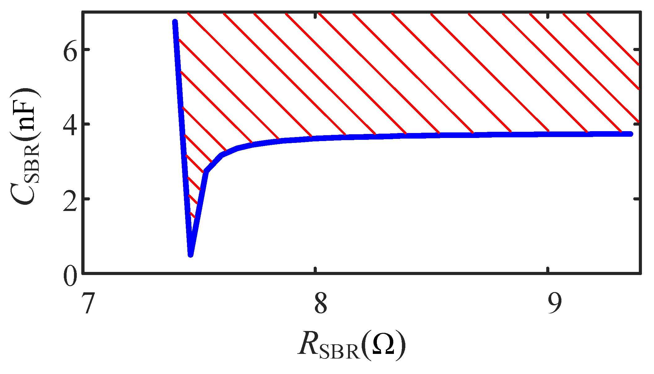
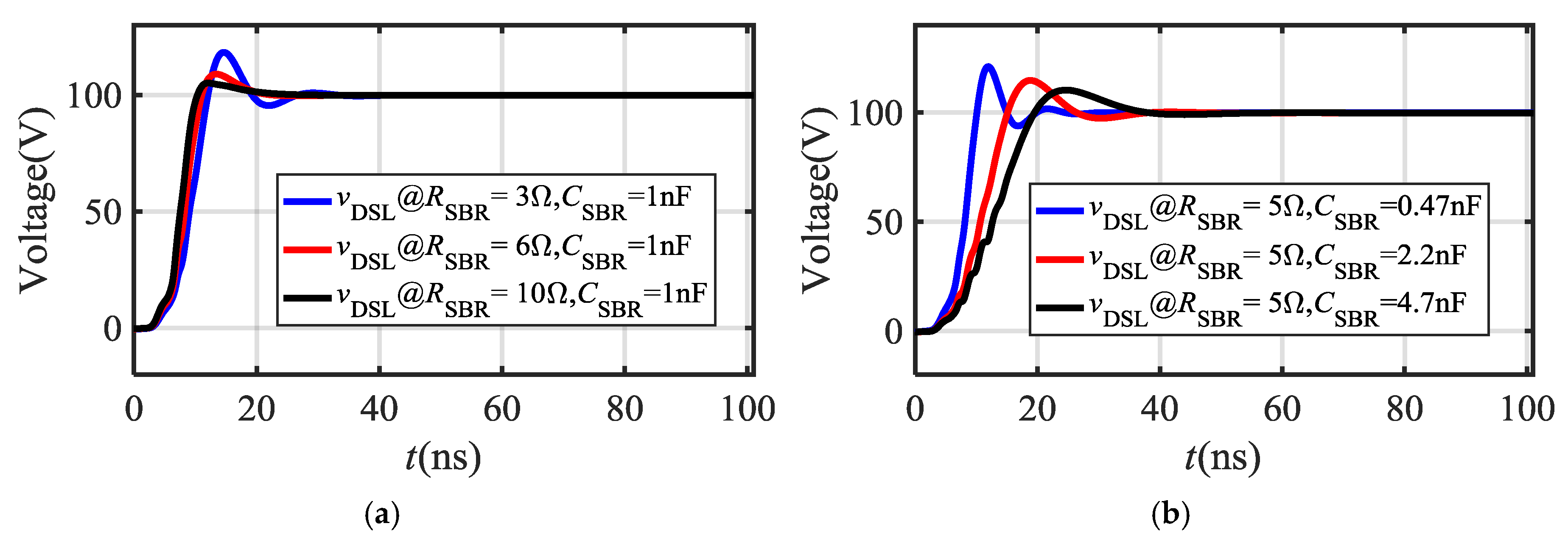
4. RC Snubber for Suppression of Parasitic Ringing
5. Results and Discussion
5.1. Simulation Results
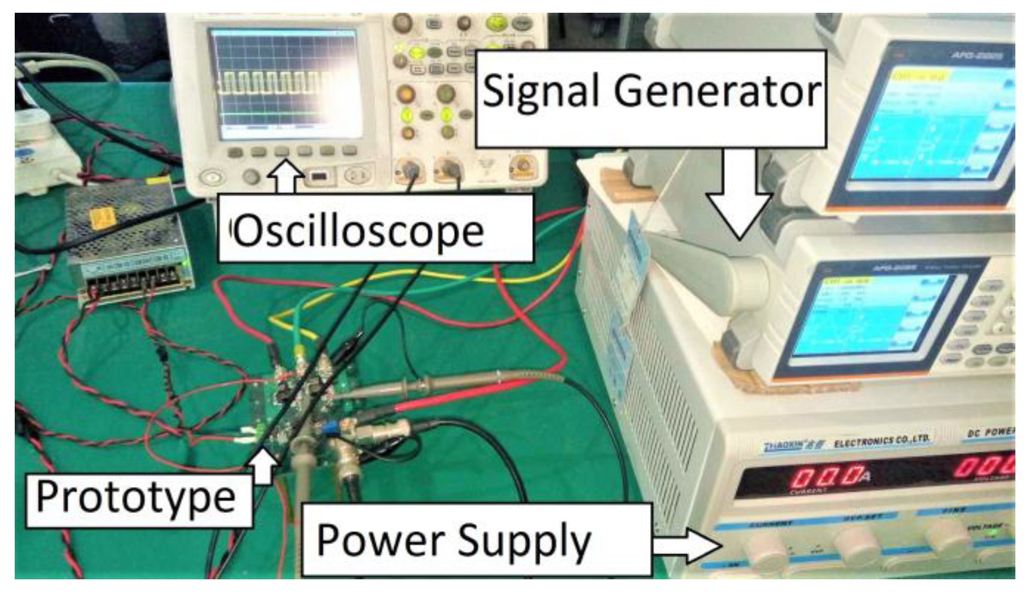
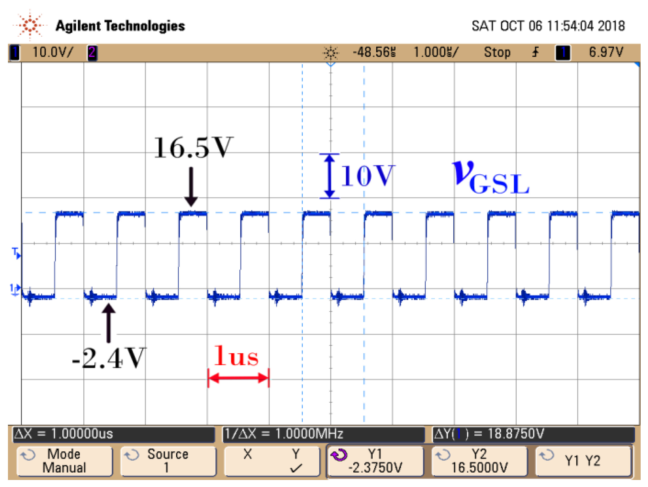
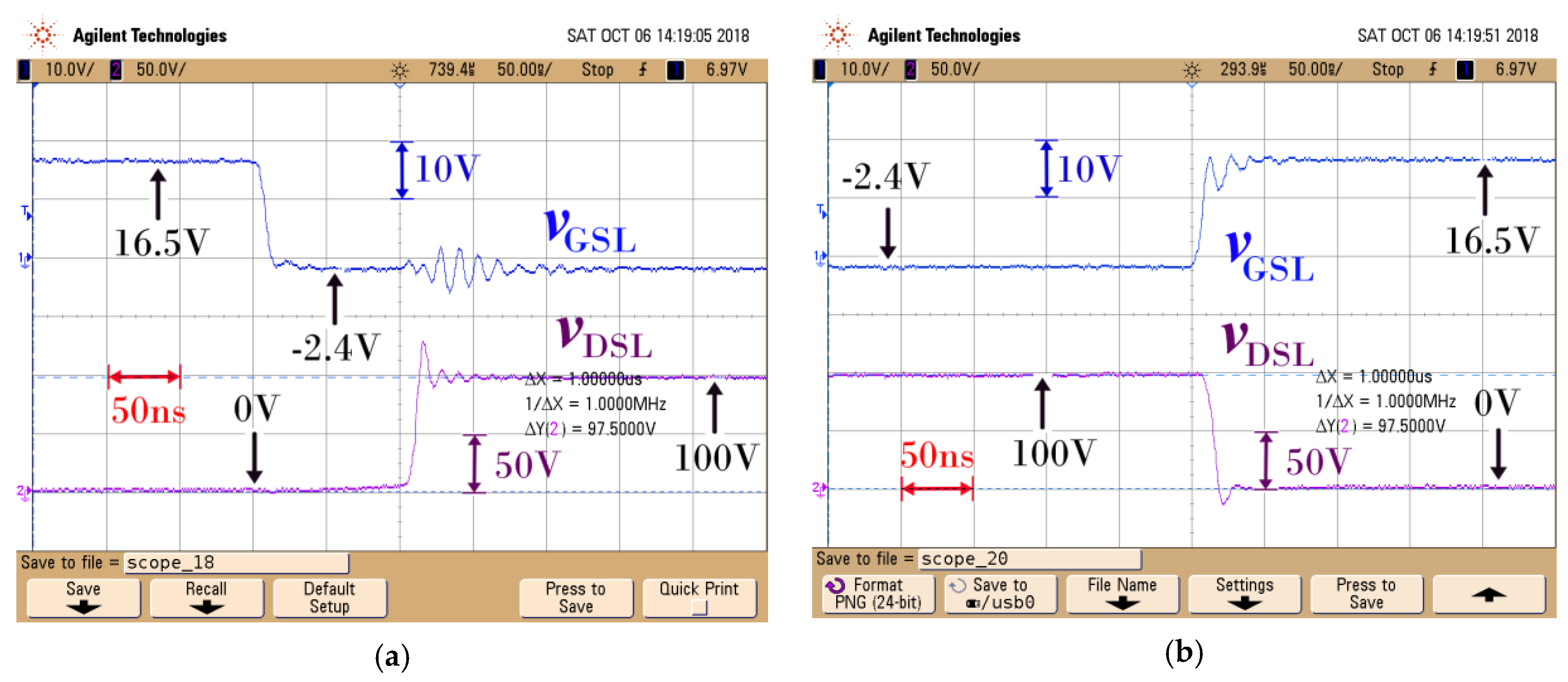
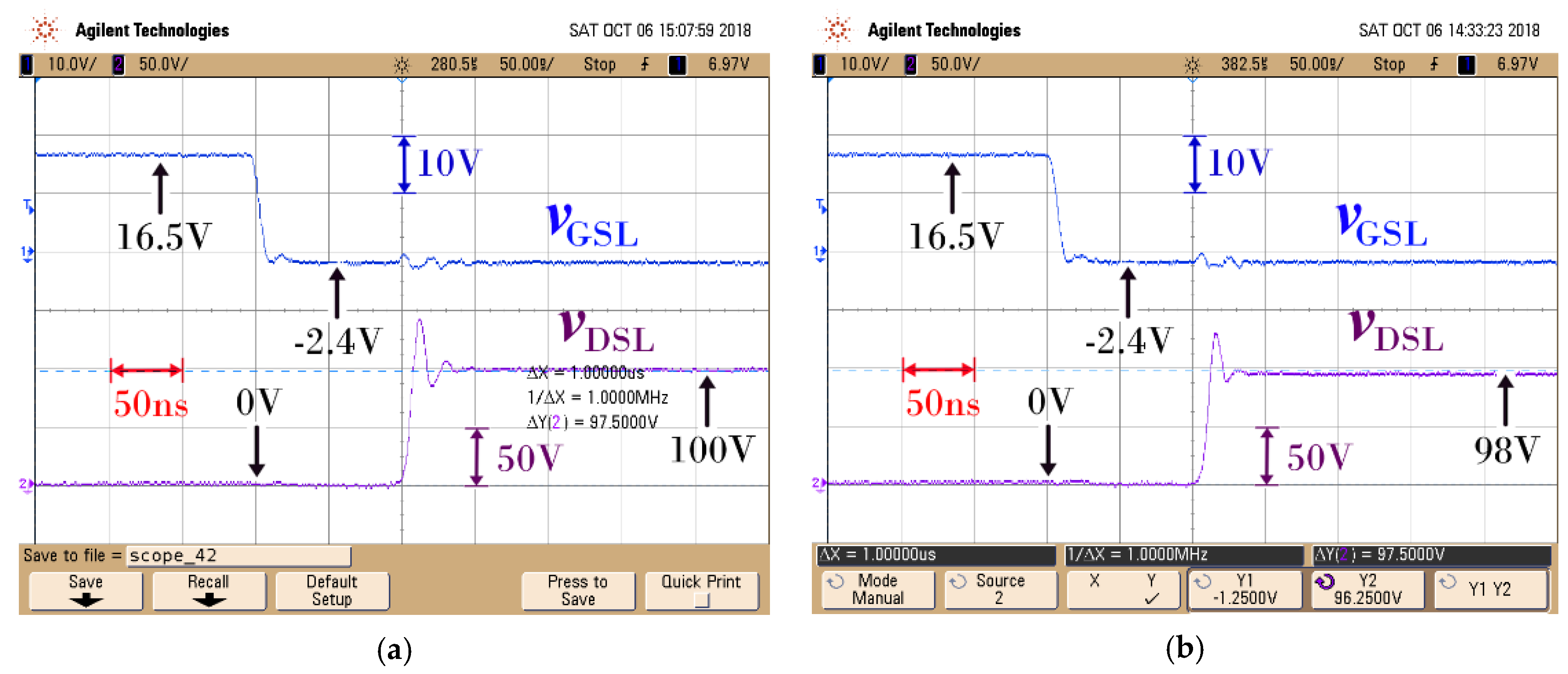
5.2. Experimental Results
5.3. Limitations of the Proposed Gate Driver and the Snubber Design Technique
6. Conclusions
Author Contributions
Conflicts of Interest
Nomenclature
| VIN | Source voltage |
| C | Output stage capacitor filter |
| C1/C2 | DC-link capacitors |
| L | Output stage inductor filter |
| R | Load resistance |
| fs/Ts | Switching frequency/switching time period |
| VTH | Threshold voltage |
| VMIL | Miller voltage |
| SL/SH | Low-side/high-side MOSFET of half-bridge converter |
| RONL/RONH | Conduction resistance of low-side/high-side MOSFET |
| CGSL/CGSH | Parasitic gate-source capacitance of low-side/high-side MOSFET |
| CDGL/CDGH | Parasitic drain-gate capacitance of low-side/high-side MOSFET |
| CDSL/CDSH | Parasitic drain-source capacitance of low-side/high-side MOSFET |
| LDL/LDH | Parasitic drain inductance of low-side/high-side MOSFET |
| LSL/LSH | Parasitic source inductance of low-side/high-side MOSFET |
| RGL(in)/RGH(in) | Internal gate resistance of low-side/high-side MOSFET |
| R1L/RTL | External gate turn-on/turn-off resistance of low-side MOSFET |
| DZPL/DZNL | Zener diode for positive/negative overvoltage gate protection |
| CZL/DZL | Capacitor/zener diode of the Level shifter circuit |
| vN/VZ | Voltage across CZL/zener voltage of DZL |
| VG | Gate driver supply voltage |
| LG | Parasitic gate inductance |
| vGSL/vGSH | Gate-source voltage of low-side/high-side MOSFET |
| vDSL/vDSH | Drain-source voltage of low-side/high-side MOSFET |
| iDL/iDH | Drain-source current of low-side/high-side MOSFET |
| iGPL/iGNL | Low-side gate current in turning-on/turning-off of MOSFET |
| iCL/iZL | Current through CZL/DZL |
| Dm | Maximum duty cycle |
| τa/τb | Time constant of gate loop during turn-on when (vN < VZ)/(vN = VZ) |
| τc | Time constant of gate loop during turn-off |
| iSBR/ISBR | Snubber current in time-domain/s-domain |
| gfs | transconductance of MOSFET |
| ωr/ζ | Parasitic resonance frequency/damping factor |
| RSBR/CSBR | Snubber resistor/capacitor |
| RC1/RC2 | Equivalent series resistance of C1/C2 |
| WBG | Wide band-gap devices |
| GaN | Gallium Nitride |
| SiC | Silicon carbide |
| THD | Total harmonic distortion |
| PCB | Printed circuit board |
| EMI | Electromagnetic interference |
| RC | Resistor-capacitor |
References
- Li, K.; Evans, P.; Johnson, M. SiC/GaN power semiconductor devices: a theoretical comparison and experimental evaluation under different switching conditions. IET Electr. Syst. Transp. 2018, 8, 3–11. [Google Scholar] [CrossRef]
- Jung, D.Y.; Park, Y. Design and Evaluation of Cascode GaN FET for Switching Power Conversion Systems. ETRI J. 2017, 39, 62–68. [Google Scholar] [CrossRef]
- Logan, T.; McMahon, R.; Hari, N. Design considerations for 600 V GaN cascode based half-bridge converter systems for utility based applications. In Proceedings of the 2016 IET International Conference on Power Electronics, Machine and Drives, Glasgow, UK, 19–21 April 2016; pp. 1–6. [Google Scholar]
- Yamaguchi, K.; Sasaki, Y.; Imakubo, T. Low loss and low noise gate driver for SiC-MOSFET with gate boost circuit. In Proceedings of the 2014 Annual Conference of the IEEE Industrial Electronics Society, Dallas, TX, USA, 29 October–1 November 2014; pp. 1594–1598. [Google Scholar]
- Peftitsis, D.; Rabkowski, J. Gate and Base Drivers for Silicon Carbide Power Transistors: An Overview. IEEE Trans. Power Electron. 2016, 31, 7194–7213. [Google Scholar] [CrossRef]
- Camacho, A.P.; Sala, V.; Ghorbani, H.; Martinez, J.L.R. A Novel Active Gate Driver for Improving SiC MOSFET Switching Trajectory. IEEE Trans. Ind. Electron. 2017, 64, 9032–9042. [Google Scholar] [CrossRef]
- Zeng, Z.; Li, X. Comparative Study on Multiple Degrees of Freedom of Gate Drivers for Transient Behavior Regulation of SiC MOSFET. IEEE Trans. Power Electron. 2018, 33, 8754–8763. [Google Scholar] [CrossRef]
- Wu, T. Cdv/dt induced turn-on in synchronous buck regulators. Int. rectifier Tech. Rep. 2007, 2, 2–7. [Google Scholar]
- Li, H.; Liao, X.; Hu, Y.; Huang, Z.; Wang, K. Analysis of voltage variation in silicon carbide MOSFETs during turn-on and turn-off. Energies 2017, 10, 1456. [Google Scholar] [CrossRef]
- Chen, H.; Divan, D. High speed switching issues of high power rated silicon-carbide devices and the mitigation methods. In Proceedings of the 2015 IEEE Energy Conversion Congress and Exposition, Montreal, QC, Canada, 20–24 September 2015; pp. 2254–2260. [Google Scholar]
- Zaman, H.; Zheng, X.; Yang, M.; Ali, H.; Wu, X. A SiC MOSFET based high efficiency interleaved boost converter for more electric aircraft. J. Power Electron. 2018, 18, 23–33. [Google Scholar]
- Liu, H.; Huang, X.; Lin, F.; Yang, Z. Loss Model and Efficiency Analysis of Tram Auxiliary Converter Based on a SiC Device. Energies 2017, 10, 2018. [Google Scholar] [CrossRef]
- Zheyu, Z.; Wang, F. Active gate driver for fast switching and cross-talk suppression of SiC devices in a phase-leg configuration. In Proceedings of the 2015 IEEE Applied Power Electronics Conference and Exposition, Charlotte, NC, USA, 15–19 March 2015; pp. 774–781. [Google Scholar]
- Abbatelli, L.; Brusca, C.; Catalisano, G. Application note: How to fine tune your SiC MOSFET gate driver to minimize losses. Available online: https://www.stmicroelectronics.com.cn/content/ccc/resource/technical/document/application_note/7d/2b/9d/f0/88/07/4b/6f/DM00170577.pdf/files/DM00170577.pdf/jcr:content/translations/en.DM00170577.pdf (accessed on 7 June 2017).
- Wang, J.; Chung, H.S.H. A novel RCD level shifter for elimination of spurious turn-on in the bridge-leg configuration. IEEE Trans. Power Electron. 2015, 30, 976–984. [Google Scholar] [CrossRef]
- Zhou, Q.; Gao, F.; Jiang, T. A gate driver of SiC MOSFET with passive triggered auxiliary transistor in a phase-leg configuration. In Proceedings of the 2015 Energy Conversion Congress and Exposition, Montreal, QC, Canada, 20–24 September 2015; pp. 7023–7030. [Google Scholar]
- Noppakunkajorn, J.; Han, D.; Sarlioglu, B. Analysis of high-speed PCB with SiC devices by investigating turn-off overvoltage and interconnection inductance influence. In Proceedings of the 2014 Applied Power Electronics Conference and Exposition, Fort Worth, TX, USA, 16–20 March 2014; pp. 2628–2634. [Google Scholar]
- Qin, H.; Ma, C.; Zhu, Z.; Yan, Y. Influence of parasitic parameters on switching characteristics and layout design considerations of SiC MOSFETs. J. Power Electron. 2018, 18, 1255–1267. [Google Scholar]
- Chen, Z.; Yao, Y.; Boroyevich, D.; Ngo, K.; Mattavelli, P. Exploration of a switching loop snubber for parasitic ringing suppression. In Proceedings of the 2014 IEEE Energy Conversion Congress and Exposition, Pittsburgh, PA, USA, 14–18 September 2014; pp. 1605–1612. [Google Scholar]
- Ren, Y.; Yang, X.; Zhang, F.; Tan, L.; Zeng, X. Analysis of a low-inductance packaging layout for Full-SiC power module embedding split damping. In Proceedings of the 2016 IEEE Applied Power Electronics Conference and Exposition, Long Beach, CA, USA, 20–24 March 2016; pp. 2102–2107. [Google Scholar]
- Palmer, P.R.; Zhang, J.; Zhang, X. SiC MOSFETs Connected in Series with Active Voltage Control. In Proceedings of the 2015 IEEE 3rd Workshop on Wide Bandgap Power Devices and Applications, Blacksburg, VA, USA, 2–4 November 2015; pp. 60–65. [Google Scholar]
- Huang, H.; Yang, X.; Wen, Y.; Long, Z. A switching ringing suppression scheme of SiC MOSFET by Active Gate Drive. In Proceedings of the 2016 IEEE 8th International Power Electronics and Motion Control Conference, Hefei, China, 22–26 May 2016; pp. 285–291. [Google Scholar]
- Han, D.; Sarlioglu, B. Comprehensive Study of the Performance of SiC MOSFET-Based Automotive DC-DC Converter under the Influence of Parasitic Inductance. IEEE Trans. Ind. Appl. 2016, 52, 5100–5111. [Google Scholar] [CrossRef]
- Li, L.; Ning, P.; Duan, Z.; Zhang, D.; Wen, X.; Qiu, Z. A study on the effect of DC-link decoupling capacitors. In Proceedings of the 2017 IEEE Transportation Electrification Conference and Expo, Asia-Pacific, Harbin, China, 7–10 August 2017; pp. 4845–4850. [Google Scholar]
- Kim, J.; Shin, D.; Sul, S.K. A Damping Scheme for Switching Ringing of Full SiC MOSFET by Air Core PCB Circuit. IEEE Trans. Power Electron. 2018, 33, 4605–4615. [Google Scholar] [CrossRef]
- Vaculik, P. The Experience with SiC MOSFET and Buck Converter Snubber Design. Int. J. Elect. Comput. Energ. Commun. 2014, 8, 49–54. [Google Scholar]
- Yatsugi, K.; Nomura, K.; Hattori, Y. Analytical Technique for Designing an RC Snubber Circuit for Ringing Suppression in a Phase-Leg Configuration. IEEE Trans. Power Electron. 2018, 33, 4736–4745. [Google Scholar] [CrossRef]
- Gao, F.; Zhou, Q.; Wang, P.; Zhang, C. A Gate Driver of SiC MOSFET for Suppressing the Negative Voltage Spikes in a Bridge Circuit. IEEE Trans. Power Electron. 2018, 33, 2339–2353. [Google Scholar] [CrossRef]
- Nayak, P.; Krishna, M.V.; Vasudevakrishna, K.; Hatua, K. Study of the effects of parasitic inductances and device capacitances on 1200 V, 35 A SiC MOSFET based voltage source inverter design. In Proceedings of the 2014 IEEE International Conference on Power Electronics, Drives and Energy Systems, Mumbai, India, 16–19 December 2014; pp. 1–6. [Google Scholar]
- Wang, Z.; Zhang, J.; Wu, X.; Sheng, K. Analysis of stray inductance’s influence on SiC MOSFET switching performance. In Proceedings of the 2014 IEEE Energy Conversion Congress and Exposition, Pittsburgh, PA, USA, 14–18 September 2014; pp. 2838–2843. [Google Scholar]
- Han, D.; Lee, W.; Noppakunkajorn, J.; Sarlioglu, B. Investigating the influence of interconnection parasitic inductance on the performance of SiC Based DC-DC converters in hybrid vehicles. In Proceedings of the 2014 IEEE Transportation Electrification Conference and Expo, Dearborn, MI, USA, 15–18 June 2014; pp. 1–7. [Google Scholar]
- Anthon, A.; Hernandez, J.C.; Zhang, Z.; Andersen, M.A.E. Switching investigations on a SiC MOSFET in a TO-247 package. In Proceedings of the 2014 Conference of the IEEE Industrial Electronics Society, Dallas, TX, USA, 29 October–1 November 2014; pp. 1854–1860. [Google Scholar]
- White Paper. Optimizing PCB Layout. 2014. Available online: https://epc-co.com/epc/Portals/0/epc/documents/papers/Optimizing%20PCB%20Layout%20with%20eGaN%20FETs.pdf (accessed on 7 June 2017).
- Application Note. PCB Layout Considerations for Non-Isolated Switching Power Supplies. Available online: https://www.analog.com/media/en/technical-documentation/application-notes/an136f.pdf (accessed on 7 June 2017).
- Application Note. Thermal Considerations for a Class D Amplifier 2006. Available online: https://www.maximintegrated.com/en/app-notes/index.mvp/id/3879 (accessed on 7 June 2017).
- Application Note. RC Snubber for Class-D Audio Amplifiers 2018. Available online: https://statics.cirrus.com/pubs/appNote/AN0454REV1.pdf (accessed on 7 June 2017).
- Application Note. Snubber Circuits for Power Electronics 2008. Available online: https://rudys.typepad.com/files/snubber-e-book-complete.pdf (accessed on 7 June 2017).
- Wang, X.; Shi, J.; Li, T.; Sun, Y. Active closed-loop gate voltage control method to mitigate metal-oxide semiconductor field-effect transistor turn-off voltage overshoot and ring. IET Power Electron. 2013, 6, 1715–1722. [Google Scholar] [CrossRef]
- Torsaeter, B.N.; Tiwari, S.; Lund, R.; Midtgard, M. Experimental evaluation of switching characteristics, switching losses and snubber design for a full SiC half-bridge power module. In Proceedings of the 2016 IEEE 7th International Symposium on Power Electronics for Distributed Generation Systems, Vancouver, BC, Canada, 27–30 June 2016; pp. 1–8. [Google Scholar]


| Parameter | Value |
|---|---|
| Source voltage (VIN) | 100 V |
| Capacitor (C) | 1.5 µF |
| Inductor (L) | 33 µH |
| Load Resistance (R) | 10 Ω |
| Switching frequency (fs) | 1 MHz |
| Parameter | Value |
|---|---|
| Threshold voltage | 2.1 V |
| Intrinsic gate resistance | 16 Ω |
| Maximum gate-source voltage | −8/+18 |
| Input capacitance | 350 pF |
| Output capacitance | 40 pF |
| Reverse transfer capacitance | 3 pF |
| Parameter | Value |
|---|---|
| R1L | 3 Ω |
| R2L | 3 Ω |
| DZPL | 18 V |
| DZNL | 5 V |
| CZL | 1 µF |
© 2018 by the authors. Licensee MDPI, Basel, Switzerland. This article is an open access article distributed under the terms and conditions of the Creative Commons Attribution (CC BY) license (http://creativecommons.org/licenses/by/4.0/).
Share and Cite
Zaman, H.; Wu, X.; Zheng, X.; Khan, S.; Ali, H. Suppression of Switching Crosstalk and Voltage Oscillations in a SiC MOSFET Based Half-Bridge Converter. Energies 2018, 11, 3111. https://doi.org/10.3390/en11113111
Zaman H, Wu X, Zheng X, Khan S, Ali H. Suppression of Switching Crosstalk and Voltage Oscillations in a SiC MOSFET Based Half-Bridge Converter. Energies. 2018; 11(11):3111. https://doi.org/10.3390/en11113111
Chicago/Turabian StyleZaman, Haider, Xiaohua Wu, Xiancheng Zheng, Shahbaz Khan, and Husan Ali. 2018. "Suppression of Switching Crosstalk and Voltage Oscillations in a SiC MOSFET Based Half-Bridge Converter" Energies 11, no. 11: 3111. https://doi.org/10.3390/en11113111
APA StyleZaman, H., Wu, X., Zheng, X., Khan, S., & Ali, H. (2018). Suppression of Switching Crosstalk and Voltage Oscillations in a SiC MOSFET Based Half-Bridge Converter. Energies, 11(11), 3111. https://doi.org/10.3390/en11113111