Article

Active Power Filtering Embedded in the Frequency Control of an Offshore Wind Farm Connected to a Diode-Rectifier-Based HVDC Link

by
Ashkan Nami
*,
José Luis Rodríguez Amenedo
,
Santiago Arnaltes Gómez
and
Miguel Ángel Cardiel Álvarez
Department of Electrical Engineering, Carlos III University of Madrid, 28911 Madrid, Spain
*
Author to whom correspondence should be addressed.
Energies 2018, 11(10), 2718; https://doi.org/10.3390/en11102718
Submission received: 20 September 2018 / Revised: 5 October 2018 / Accepted: 7 October 2018 / Published: 11 October 2018
(This article belongs to the Section F: Electrical Engineering)

Abstract

:
This paper presents a novel active power filtering (APF) scheme embedded in a centralised frequency control of an offshore wind farm (OWF) connected to a high voltage direct current link through a diode rectifier station. The APF is carried out by a voltage source converter (VSC), which is connected to the rectifier station to provide frequency control for the offshore ac-grid. The proposed APF scheme eliminates harmonic currents at a capacitor bank placed at the rectifier station. This leads to a significant reduction in the total harmonic distortion of the offshore ac-grid voltage, and thus, to an improvement in the OWF power. Hence, the rectifier passive ac-filter bank is not needed anymore. A new selective harmonic compensation method based on the dynamic phasor (DP) theory is used in the proposed APF scheme which allows the extraction of the phasor form of harmonics in dc-signals. Therefore, the well-known proportional-integral regulators are used for the harmonic current compensation. Moreover, the offshore ac-grid is modelled for the system harmonic analysis using a grid solution based on the DP theory. Finally, a VSC power rating analysis is studied. The performance of the proposal is validated by simulations in both steady-state and transient conditions.

1. Introduction

Recently, offshore wind farms (OWFs) have been developed due to the better offshore wind conditions. Since OWFs are planned to be located at long distances from the shore, a high voltage direct current (HVDC) transmission system is the preferable technology compared to high voltage alternating current (HVAC), for the integration of OWFs to the onshore grid [1]. Two main HVDC technologies are line-commutated converters (LCCs) that use thyristors and forced-commutated voltage source converters (VSCs) that use, in most industrial cases, insulated gate bipolar transistors (IGBTs).
The VSC-based HVDC transmission system offers more controllability, such as voltage and frequency control, for the isolated offshore ac-grid. Despite operational advantages, VSC-based HVDC has higher overall losses, is more vulnerable to line faults, and needs higher maintenance compared to LCCs [1,2]. In addition, it requires the construction of an offshore platform, further increasing the cost. Recently, various studies on OWF configurations based on series and parallel dc collection and transmission have been investigated to minimize losses and installation costs by eliminating the need for VSC offshore platforms [3,4,5]. However, such configurations require a number of conversion stages for power conversion via multiple stages of transformers and ac–dc and dc–dc stages which need to be located in one or more offshore platforms, further increasing the costs and losses. In order to overcome the aforementioned drawbacks, a new HVDC technology that integrates OWFs was proposed in [6] in which diode-rectifier-based HVDC links are employed. The new approach uses diode rectifier stations in HVDC links for OWF applications, resulting in a better performance in terms of efficiency, cost, converter size, and reliability [7].
A disadvantage of the diode rectifier solution is the lack of control for frequency in the offshore ac-grid, given that the isolated OWF grid cannot generate the required frequency for the diode rectifier commutation. Moreover, due to the missing ac-voltage source at the rectifier station defining the frequency, the conventional wind turbine (WT) converter grid synchronisation via a phase-locked loop (PLL) is unfeasible for this system. The frequency control solutions for OWFs connected to diode-rectifier-based HVDC links proposed in the literature can be classified generally into two different solutions: distributed and centralised. In distributed control solutions, the frequency control is implemented in the WTs [8,9,10], where type-4 WTs are considered because of their higher control flexibility. However, these proposals employ an indirect frequency control depending on many measurements through the OWF which causes the lack of robustness. Moreover, no communication channels are considered in the transmission of these measurements. In [11,12], a global positioning system (GPS) signal is used to provide a common angular reference for both type-3 and type-4 WTs, which leads to the synchronisation of all WTs’ current injections. In this solution, the WTs’ active power control is not affected. However, a droop control is proposed for the WTs’ voltage angle control which affects the WTs’ reactive power control. This results in a minor change in the conventional control of the WT converters. Moreover, this solution does not allow the WTs to have decoupled active and reactive power controls, since the WTs’ voltage vectors are not aligned with the reference axis. The proposal in [13] uses active power voltage (P/V) droop and reactive power frequency (Q/f) droop controls for the parallel operation of WTs, resulting in reactive power sharing among WTs. Ref. [14,15] also introduce distributed solutions using Q/f droop control for reactive power sharing among WTs. In these proposals, communication between WTs is not needed, and the second one avoids using any PLL. However, this kind of solution, which is based on droop control is not implemented in most WTs [16], whereas centralised solutions can be achieved with no changes in the conventional control of the WT converters. For this purpose, centralised solutions using an ac-voltage source at the rectifier station have been addressed in the literature. A centralised control solution is proposed in [17] in which a hybrid topology of the HVDC converter is employed. This proposal presents a 12-pulse diode rectifier with a series-connected VSC that provides one-third of the transmitted power as well as the frequency control. A modular, multilevel converter can also be used in this kind of solution to reduce the dc-voltage ripple and as a result, to reduce the size of the required dc-inductors [16]. Another centralised control solution using a reactive power source at the capacitor bank bus connected to the rectifier station is proposed in [18]. In this centralised solution, the frequency control is achieved by the reactive power balancing at the capacitor bank bus, which is provided by the reactive power source. The authors in [18] used an average value model of the diode rectifier to derive the proposed control. However, it is illustrated in [19] that a hybrid switched model better represents the actual power converter dynamics; leading to the uncertainties in the power converters’ parameters being handled by an adaptive control approach.
However, another disadvantage of the diode-rectifier-based HVDC link solution is the passive ac-filter bank at the rectifier station that is required to eliminate the harmonic currents created by the diode rectifier. Some proposals have been addressed in the literature to overcome this drawback. Ref. [20] studied the control proposed in [10] with a reduced rectifier ac-filter bank. This proposal allows WTs to inject the required reactive power for the reduction of the rectifier ac-filter bank. However, this results in a large ripple in WT currents due to their high harmonic contents. The controls proposed in [17,21] are also used to reduce the rectifier ac-filter bank by taking advantage of the active power filtering (APF) offered by the series-connected VSC. These APF schemes are used to compensate only the low-frequency harmonic currents of the rectifier. However, offshore ac-grid harmonic currents are not considered in these systems. Given the WT converters’ operation, the WTs’ currents are also considered to be harmonic current sources injected into the offshore ac-grid [22]. These harmonic currents flow into the point of common coupling (PCC) and increase total harmonic distortion (THD) of the offshore ac-grid voltage which leads to power quality degradation. Moreover, despite the APF implementation in this kind of solution, there are still passive ac-filter banks remaining at the rectifier station. Besides, the APF schemes implemented in these proposals utilise the conventional selective harmonic compensation (SHC) method based on proportional-resonant (PR) controllers. However, PR controllers are more complex, compared to the well-known proportional-integral (PI) controllers, in terms of their computational requirements [23,24]. Finally, the dynamic phasor (DP) theory can be used for harmonic consideration [25] which allows all harmonic contents of any signal to be extracted. Therefore, the DP theory can also be used to solve the static model of the offshore ac-grid at each considered harmonic needed for the harmonic analysis of the system. However, the approach proposed in [26] is used to dynamically analyse and model the power grid.
This paper presents a novel APF scheme embedded in a centralised frequency control of an OWF connected to a diode-rectifier-based HVDC link. The APF is performed by a VSC connected to the rectifier station, which is used to provide centralised frequency control for the offshore ac-grid. Concerning the harmonic currents of the offshore ac-grid, they are considered in the system harmonic analysis. Then, the proposed APF scheme is implemented to eliminate the harmonic currents at a capacitor bank placed at the rectifier station, which has not been implemented before. This leads to a significant reduction in the THD of the offshore ac-grid voltage and as a result, to an improvement in the OWF power quality. Therefore, no passive ac-filter bank is needed at the rectifier station. In this paper, a new SHC method based on the DP theory is used in the proposed APF scheme which allows the extraction of the phasor form of harmonics in dc-signals. Hence, the well-known PI controllers can be used for harmonic current compensation. In addition, a grid solution based on the DP theory is used to solve the offshore ac-grid model needed for the harmonic analysis of the system. Finally, the VSC power rating analysis is studied to select the required size for the VSC.
The paper is organised as follows. The considered OWF structure and its simplified model are presented in Section 2. In Section 3, the harmonic analysis of the system is carried out to justify the harmonic currents to be compensated in the APF scheme. The proposed control scheme needed for the VSC is presented in Section 4. The VSC power rating is analysed in Section 5. In Section 6, the simulation results are presented to validate the proposed control scheme. Finally, the conclusions are addressed in Section 7.

2. System Description and Modelling

Figure 1a shows the considered OWF, consisting of a number of WTs which can be type-3 or type-4. The WTs are connected to the offshore ac-grid through the WT transformers ( T w t ). The OWF transformers ( T o w f ), interconnecting the WTs clusters, are used to step-up the mid-voltage distribution offshore ac-grid. A twelve-pulse diode rectifier, representing the offshore HVDC link access, is connected to the offshore ac-grid at the PCC by means of the rectifier transformer ( T r e c ). A required capacitor bank (C) for reactive power compensation of the diode rectifier and its transformer is connected to the PCC. A VSC is placed at the rectifier station connected to the capacitor bank bus which is used for the offshore ac-grid frequency control as well as the APF. The onshore HVDC inverter can include LCC or VSC-based technology, but it has to be operated in constant dc-voltage control mode.
Note that, given the APF provided by the VSC, the passive ac-filter bank at the rectifier station is not needed.
Figure 1b shows a simplified model of the OWF depicted in Figure 1a. Given that the conventional WT converters’ grid synchronisation via PLL is feasible in this system because of the centralised frequency control provided by the VSC, the WTs are represented by the controlled current sources. Hence, the WTs’ output powers are provided by current injection to the OWF grid. A static model of the OWF is used for the harmonic analysis of the offshore ac-grid. Therefore, a grid solution based on the DP theory (described in Section 3) is used to define the WTs’ bus voltages ( v k ) and the OWF grid current ( i o w f ) at each considered harmonic by using the WTs’ currents ( i k ) and the capacitor bank voltage ( u c ) as inputs. The VSC model is represented by a controlled voltage source ( v v s c ) with its corresponding impedance ( L f and R f ). The HVDC link is modelled using an accurate dc-cable model for the dc transmission line proposed in [27], which is connected in series on both sides with the dc smoothing reactor depicted by L s and R s . The HVDC onshore inverter station is modelled as a controlled current source with a parallel-connected DC capacitor ( C d c i n v ). Therefore, the onshore inverter model is controlled in a way that regulates the C d c i n v voltage; resulting in the HVDC link power being injected into the onshore grid.
Due to the missing controlled frequency in the isolated offshore ac-grid, the conventional VSC grid synchronisation via PLL becomes unfeasible without frequency control. Thus, the analysis of the offshore ac-grid shown in Figure 1b is carried out in a synchronous ( d q ) reference frame rotating at a desired frequency (50 Hz) provided by a reference source. For this purpose, the dynamics of the simplified model in Figure 1b in the d q reference frame rotating at ω 0 are written as follows:
C d u d c d t = i d o w f + i d v s c i d r e c + C ω 0 u q c
C d u q c d t = i q o w f + i q v s c i q r e c C ω 0 u d c
L f d i d v s c d t = v d v s c u d c R f i d v s c + L f ω 0 i q v s c
L f d i q v s c d t = v q v s c u q c R f i q v s c L f ω 0 i d v s c .
Without frequency control, given that no PLL is used, the capacitor bank voltage vector is not aligned with the reference axis and as a result, its q-component is not zero ( u q c 0 ). According to Equation (2), the VSC’s q-axis current ( i q v s c ) can be used to control the q-component of the capacitor bank voltage ( u q c ). i q v s c is controlled to follow the desired reference with the conventional current controller in order to orient the capacitor bank voltage vector along the d axis ( u q c = 0 ). As a result, given that the synchronous axis rotates at the desired frequency, frequency control will be achieved [18]. The VSC d-axis current ( i d v s c ) is used to regulate the VSC dc-voltage. Therefore, the d-component of the capacitor bank voltage ( u d c ) defining the offshore ac-grid voltage depends on the active power transmitted by the HVDC link at steady-state, in accordance with Equation (1).
However, OWF d-q currents ( i d o w f and i q o w f ) and diode rectifier ac-side d-q currents ( i d r e c and i q r e c ) contain harmonic components because of both the WT converters’ operation and the diode rectifier functionality, respectively. These harmonic currents distort the offshore ac-grid voltage when flowing into the capacitor bank, as shown by Equations (1) and (2). Therefore, compensated currents can be injected through i d v s c and i q v s c to eliminate the harmonic contents of the capacitor bank current which leads to THD reduction of the offshore ac-grid voltage. For this purpose, analytical expressions in the d q reference frame for both i o w f and i r e c are expanded in Section 3 to justify the compensation of the system’s harmonic contents.

3. System Harmonic Analysis

3.1. Offshore ac-Grid Current

The WTs’ currents injected into the offshore ac-grid generally contain harmonics because of the WT converters’ operation. Therefore, the general expression of the kth WT current, i k ( t ) , in a balanced three-phase system can be written as follows:
i a , b , c k ( t ) = h = 1 H I h k cos ( h ω 0 t + φ h k + γ h )
where γ h equals zero for phase a, h 2 π 3 for phase b, and h 2 π 3 for phase c; k denotes the number of WTs; I h k is the amplitude value of the hth-order harmonic current injected by the kth WT, and φ h k is its phase angle; H is the highest considered harmonic order; and ω 0 is the fundamental angular frequency of the system.
The Park transformation shown in Equation (6) defines the kth WT current vector i ̲ k ( t ) in the d q reference frame rotating at the fundamental frequency ω 0 .
i ̲ k ( t ) = 2 3 ( i a k ( t ) + a ̲ i b k ( t ) + a ̲ 2 i c k ( t ) ) · e j ω 0 t
where a ̲ = e j 2 π / 3 and a ̲ 2 = e j 2 π / 3 .
By combining Equations (5) and (6), i ̲ k ( t ) can be analytically expressed as follows:
i ̲ k ( t ) = I ̲ 1 k + h = 2 H I ̲ h k e j ( h 1 ) ω 0 t ( A 3 ) + I ̲ h k * e j ( h + 1 ) ω 0 t ( B 3 )
where A = 1 + e j ( h 1 ) 2 π / 3 + e j ( h 1 ) 2 π / 3 and B = 1 + e j ( h + 1 ) 2 π / 3 + e j ( h + 1 ) 2 π / 3 , I ̲ 1 k and I ̲ h k are the fundamental and hth-order harmonic current vectors injected by the kth WT, respectively, and * denotes the complex conjugate operator.
Hence, the simplified form of Equation (7) can be written as
i ̲ k ( t ) = I ̲ 1 k + n = 1 I ̲ ( 3 n + 1 ) k e j 3 n ω 0 t + I ̲ ( 3 n 1 ) k * e j 3 n ω 0 t
where ( n = 1 , 2 , 3 , ) .
According to Equation (8), each WT current vector in the d q reference frame contains triple harmonics, 3 n ω 0 . These triple harmonics refer to ( 3 n ± 1 ) ω 0 harmonics in the stationary reference frame ( α β ) at the fundamental frequency. The harmonic order h = 3 n + 1 ( h = 4 , 7 , 10 , ) is the positive sequence, whereas the harmonic order h = 3 n 1 ( h = 2 , 5 , 8 , ) is the negative sequence.
In order to take these harmonic currents into account, I ̲ ( 3 n + 1 ) k and I ̲ ( 3 n 1 ) k * need to be defined individually for each WT. For this purpose, the ratios of their magnitudes to the fundamental current vector magnitude determined in [22] are used to define the magnitude values of I ̲ ( 3 n + 1 ) k and I ̲ ( 3 n 1 ) k * . These ratios are listed in a table shown in Appendix A. Concerning the phase angle values of I ̲ ( 3 n + 1 ) k and I ̲ ( 3 n 1 ) k * , they are defined randomly.
Note that, both the magnitude and phase angle values of I ̲ 1 k are determined individually for each WT by
I ̲ 1 k = 2 3 1 V 1 k P k 2 + Q k 2 · e j ( θ 1 k arctan ( Q k / P k ) )
where P k and Q k are the kth WT active and reactive powers, respectively, V 1 k is the magnitude of the kth WT fundamental bus voltage vector, and θ 1 k is its phase angle.
Moreover, in order to define all harmonic contents of the WTs’ bus voltages ( v k ) and the OWF current ( i o w f ), a harmonic grid solution is used for the static model of the offshore ac-grid. This solution is carried out separately at each harmonic frequency as well as at the fundamental frequency using the WTs’ currents ( i k ) and the capacitor bank voltage ( u c ) as inputs. This leads to v k and i o w f being defined at all considered frequencies. The required matrix expression for this grid solution is as follows:
[ v ̲ h 1 v ̲ h k v ̲ h N 1 i ̲ h owf ] = [ M ( h ) ] [ i ̲ h 1 i ̲ h k i ̲ h N 1 u ̲ h c ]
where h equals 1, 2, 4, 5, …H; N is the number of nodes of the offshore ac-grid; v ̲ h k is the hth-order harmonic voltage vector at node k (kth WT bus); i ̲ h owf is the OWF hth-order harmonic current vector; i ̲ h k is the hth-order harmonic current vector injected at node k (by kth WT); u ̲ h c is the capacitor bank hth-order harmonic voltage vector; and M ( h ) is defined as a combination of admittance and impedance matrices of the grid at the hth-order harmonic frequency, which is detailed in Appendix B.
Finally, the kth WT bus voltage vector v ̲ k ( t ) and OWF current vector i ̲ owf ( t ) are defined by the summation of all of their vector elements at different frequencies, given by Equation (10) as follows:
v ̲ k ( t ) = V ̲ 1 k + h = 2 H v ̲ h k ( t ) , i ̲ owf ( t ) = I ̲ 1 owf + h = 2 H i ̲ h owf ( t )
where h = 2 , 4 , 5 , 7 , H , V ̲ 1 k and v ̲ h k ( t ) are the fundamental and hth-order harmonic voltage vectors at the kth WT bus, respectively, and I ̲ 1 owf and i ̲ h owf ( t ) are the fundamental and hth-order harmonic current vectors of the OWF, respectively.
However, u ̲ h c must be provided for the grid solution. For this purpose, a method based on the DP theory is proposed to extract u ̲ h c from the capacitor bank voltage vector ( u ̲ c ).
The DP theory is based on Fourier series expansion. A time-domain waveform x ( τ ) is considered over the interval τ ( t T , t ] to be periodic and is represented using the Fourier series as follows:
x ( τ ) = h = x h ( t ) · e j h ω 0 τ
where
x h ( t ) = 1 T t T t x ( τ ) · e j h ω 0 τ d τ
is its hth complex Fourier coefficient and is referred to as a DP. The selected number of DPs defines the approximation accuracy of the waveform.
Moreover, the following conjugate property for real x ( τ ) proves to be useful:
x h = x h * .
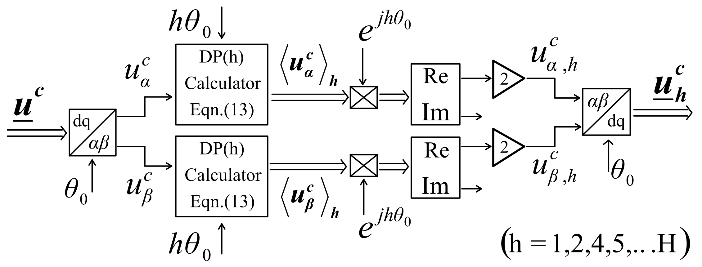
Figure 2 shows the diagram of the proposed technique to provide u ̲ h c . As it can be observed, u ̲ c is transformed into the α β reference frame to allow the extraction of u ̲ h c individually at all considered positive and negative sequences of harmonic frequencies ( h = 3 n ± 1 with n = 1 , 2 , ). The proposed method is implemented similarly on both α - β capacitor bank voltages ( u α c and u β c ) to provide the corresponding components of the capacitor bank’s hth-order harmonic voltage vector in the α β reference frame ( u α , h c and u β , h c ). For this purpose, the DP calculator based on Equation (13) is used separately for both α and β channels to extract the hth-order harmonic component from both u α c and u β c . Therefore, the DP calculator output in each channel provides the phasor of the extracted hth-order harmonic component at its frequency (its reference frame) for the corresponding channel ( u α c h and u β c h ). Moreover, both u α c h and u β c h need to be transformed from their reference frame into the original reference frame of their DP calculators inputs ( α β reference frame here). According to Equation (12), additional DP calculators at considered negative frequencies ( h ) are also needed in each channel for the required transformation. However, according to the conjugate property shown in Equation (14), the required transformation can be simplified. This is carried out by multiplying both u α c h and u β c h by e j h θ 0 in both channels, and a two-fold multiplication of the real component of their product provides both u α , h c and u β , h c . Finally, the capacitor bank’s hth-order harmonic voltage vector in the α β reference frame is transformed into the d q reference frame to provide u ̲ h c .

3.2. Rectifier ac-Current

According to the diode rectifier functionality, the three-phase rectifier ac-currents i a , b , c r e c ( t ) can be determined by modulating the rectifier dc-current i d c r e c ( t ) with the three-phase twelve-pulse current switching functions S i a , b , c 12 P ( t ) as follows:
[ i a r e c i b r e c i c r e c ] = i d c r e c [ S i a 12 P S i b 12 P S i c 12 P ] .
Since the analytical expression, assuming balanced operating conditions and diode commutation process, for the six-pulse current switching function is known [28], the frequency-domain expression of S i a , b , c 12 P ( t ) can be analytically obtained (detailed in Appendix C). The result is shown in Equation (16).
S i a , b , c 12 P ( t ) = 4 3 π { n = 0 k ( 12 n + 1 ) cos ( ( 12 n + 1 ) ( ω 0 t μ 2 + γ ) ) n = 1 k ( 12 n 1 ) cos ( ( 12 n 1 ) ( ω 0 t μ 2 + γ ) ) }
where γ equals zero for phase a, 2 π 3 for phase b and 2 π 3 for phase c, k ( 12 n ± 1 ) = sin ( ( 12 n ± 1 ) μ / 2 ) ( 12 n ± 1 ) 2 μ / 2 , and μ is the diode commutation angle.
On the other hand, the rectifier ac-voltage ( u c ) generally contains harmonics, as the OWF harmonic currents flow into the capacitor bank and distort its voltage. Based on the modulation theory, the rectifier dc side voltage v d c r e c ( t ) is determined from the distorted ac-voltage u c in the frequency-domain. The result is a Fourier expression of v d c r e c ( t ) which contains the triple harmonic components h = 3 n ( n = 1 , 2 , ) [28]. Since the rectifier dc-current ( i d c r e c ( t ) ) is determined from v d c r e c ( t ) , the general expression of this current is as follows:
i d c r e c ( t ) = I d c , 1 r e c + n = 1 I d c , 3 n r e c cos ( 3 n ω 0 t + φ d c , 3 n r e c )
where I d c , 1 r e c is the dc component of the rectifier dc-current, I d c , 3 n r e c is the amplitude value of the 3 n th-order harmonic current, and φ d c , 3 n r e c is its phase angle. Note that, the values of these variables depend on the rectifier dc side parameters.
Similarly, the rectifier ac-current vector i ̲ rec ( t ) in the d q reference frame can be derived as follows:
i ̲ rec ( t ) = 2 3 ( i a r e c ( t ) + a ̲ i b r e c ( t ) + a ̲ 2 i c r e c ( t ) ) · e j ω 0 t .
According to Equations (16) and (18), i ̲ rec ( t ) can be generally expressed in the following symbolic form:
i ̲ rec ( t ) = I ̲ 1 rec + n = 1 I ̲ ( 3 n + 1 ) rec e j 3 n ω 0 t + I ̲ ( 3 n 1 ) rec * e j 3 n ω 0 t
where I ̲ 1 rec is the fundamental current vector of the rectifier ac-current, I ̲ ( 3 n + 1 ) rec and I ̲ ( 3 n 1 ) rec are the positive and negative sequence harmonic current vectors of the rectifier ac-current, respectively, and * denotes the complex conjugate operator. Analytical expressions for these variables, assuming no harmonic currents are present on the rectifier dc side, are available in Appendix D.
As can be observed, the rectifier ac-current vector in the d q reference frame contains triple harmonics, referring to both corresponding positive and negative sequence harmonics in the α β reference frame.
Finally, in accordance with Equations (8) and (19), the system’s harmonic currents flowing into the capacitor bank (C) contain triple-order harmonics in the d q reference frame. Therefore, the THD of the offshore ac-grid voltage can be reduced by elimination of the triple harmonic components of the capacitor bank current in the d q reference frame. It should be pointed out that, due to the missing PLL, the measured capacitor bank current needed for harmonic compensation can be transformed into the d q reference frame independently from any measurement noise or grid disturbance.

4. Control Strategy

As described before, both the offshore ac-grid frequency control and the APF are performed by the VSC placed at the rectifier station. For this purpose, the required VSC control strategy is presented in this section.
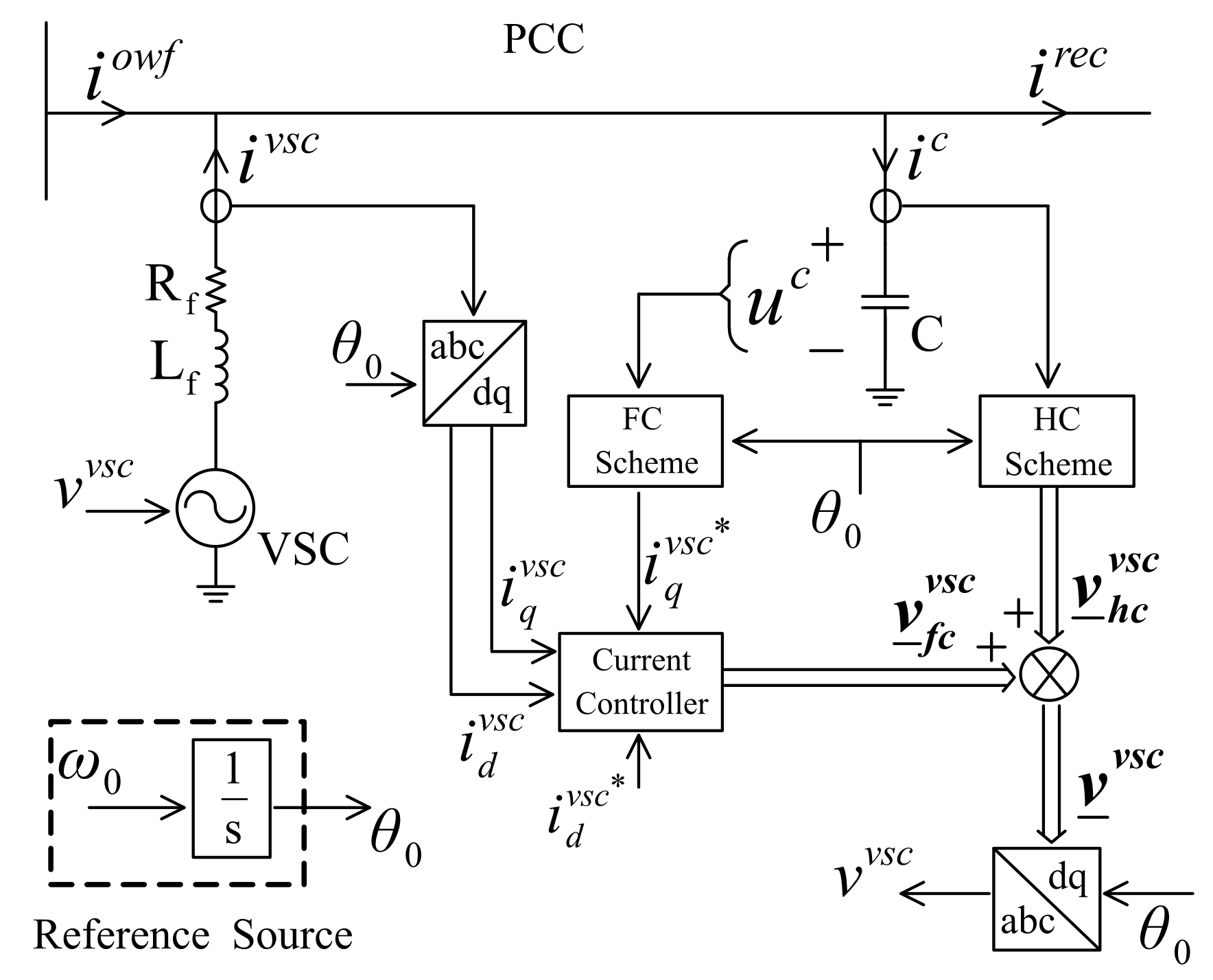
The overall scheme of the proposed control strategy is depicted in Figure 3. The voltage angular position θ 0 needed for the VSC control implementation is obtained by the integration of a desired fixed angular frequency ω 0 through a reference source. Due to the missing PLL, the reference angular position is entirely independent of measurement noise and grid disturbance. Therefore, the proposed control strategy can be implemented in the d q reference frame rotating at the fundamental frequency (50 Hz) provided by the reference source.
The centralised offshore ac-grid frequency control is implemented in the frequency control (FC) scheme and its output defines the VSC q-axis current reference i q v s c * . On the other hand, the VSC d-axis current reference i d v s c * is set by the dc-voltage regulation of the VSC [29]. For this purpose, the dynamics of the converter dc capacitance are considered in the VSC model where the VSC dc-voltage is regulated through its d-axis current. Hence, the VSC d-q currents ( i d v s c and i q v s c ) are controlled to follow their references with the conventional current controller loops [29]. The output of the current controller provides the required VSC voltage vector for the frequency control ( v ̲ fc vsc ). Moreover, the harmonic compensation (HC) scheme is assigned to compensate the capacitor bank harmonic currents, and its output provides the required VSC voltage vector for the harmonic compensation ( v ̲ hc vsc ). Then, the total required VSC voltage vector for both the APF and the frequency control ( v ̲ vsc ) is provided by the summation of v ̲ fc vsc and v ̲ hc vsc .
In the following subsections, both the FC and the HC schemes are described.

4.1. Centralised Frequency Control

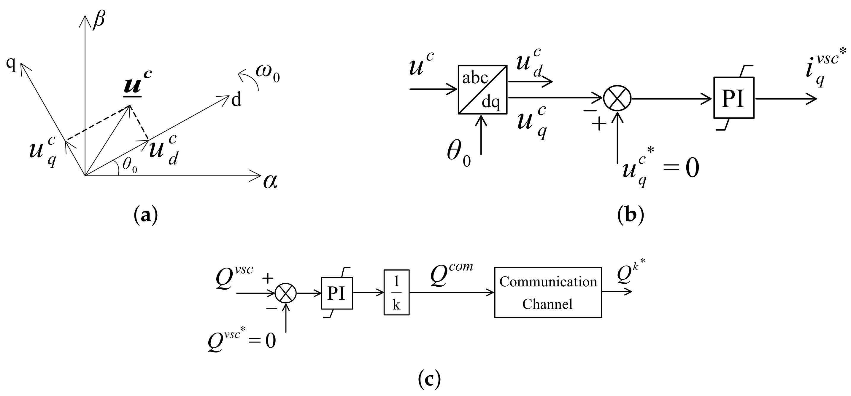
Figure 4a shows the capacitor bank voltage vector u ̲ c in the d q reference frame rotating at the fundamental frequency ( ω 0 ), which is provided by the reference source. Given that the reference d q axis has the desired frequency (50 Hz), the offshore ac-grid frequency control can be achieved by aligning the capacitor bank voltage vector along the d axis ( u q c = 0 ). For this purpose, the q-component of the capacitor bank voltage ( u q c ) is controlled by the VSC q-axis current i q v s c , in accordance with Equation (2). Therefore, the VSC is employed to inject the required reactive power into the capacitor bank bus to achieve frequency control.
The required VSC reactive power for the frequency control is defined by the FC scheme shown in Figure 4b. As can be observed, the q-component of the capacitor bank voltage ( u q c ) is controlled to be zero with a PI controller, and its output sets the VSC q-axis current reference i q v s c * . Note that, the d-component of the capacitor bank voltage u d c which defines the magnitude of the offshore ac-grid voltage remains uncontrolled, since the HVDC-diode rectifier acts as a voltage clamp on u d c .
However, the steady-state reactive power required for the VSC could be high which would cause an increment in the reactive power capability of the VSC, while the WTs’ reactive power capability could be used instead. Therefore, the control scheme presented in Figure 4c is used to make the WT converters provide the required steady-state reactive power through sending a reactive power command to the WTs. As a result, the VSC will not supply the steady-state reactive power needed for the frequency control.
For this purpose, as shown in Figure 4c, the VSC reactive power ( Q v s c ) is regulated to zero with a PI controller. Then, in order to provide equal sharing of the required steady-state reactive power among the WTs, the output of the controller is divided by a constant (k) that is proportional to the number of WTs. This results in the provision of the required reactive power command ( Q c o m ) for the WTs. Finally, Q c o m is sent through a communication channel to the WTs to define the reactive power reference of each WT ( Q k * ). Note that, the communication channel is modelled as a time delay of 0.1 s to postpone the signal reception.

4.2. Harmonic Compensation

Figure 5a shows a diagram of the HC scheme. Since the capacitor bank current contains well-known harmonic orders (as described in Section 3), a new SHC method based on the DP theory is used in the HC scheme. As shown, the SHC is implemented similarly for both capacitor bank d-q currents ( i d c and i q c ) to provide the required VSC d-q voltages for the harmonic compensation ( v h c , d v s c and v h c , q v s c ).
The diagram of the proposed SHC is depicted in Figure 5b. A waveform x is considered to be an input of the diagram which can be either i d c or i q c . Therefore, according to the analytical expressions expanded in Section 3, the waveform x contains triple harmonics 3 n ω 0 ( n = 1 , 2 , ) . The proposed SHC is implemented individually for all harmonics of x to provide the required waveforms for compensation of the corresponding harmonics ( y h c , 3 n ). For this purpose, the DP calculators at triple harmonic frequencies extract the phasor form of all harmonics of x at their frequencies ( x 3 n ). Therefore, both real and imaginary components of each extracted harmonic phasor are provided in dc-signals. Then, they are regulated separately to zero with PI controllers to eliminate the corresponding harmonic from x. Moreover, the PI regulators’ outputs from each SHC process provide the phasor form of the required waveforms for compensation of the corresponding harmonics at their frequencies ( y hc 3 n ). In order to provide y h c , 3 n , these obtained phasors are transformed from their reference frames into the original reference frame of the DP calculator’s inputs ( d q reference frame here) in accordance with Equations (12) and (14). Finally, the summation of all elements of y h c , 3 n determines the required waveform for compensation of all considered harmonic orders ( y h c ) which can be either v h c , d v s c or v h c , q v s c .

5. VSC Power Rating Analysis

Since the VSC is employed as a STATCOM in such applications, the required VSC reactive power for the frequency control affects the power rating of the VSC. However, the steady-state reactive power required for the VSC is zero thanks to sending the required reactive power command to the WTs. Therefore, the required reactive power capability of the VSC depends on the transients in the system and the control and system parameters, e.g., the OWF active and reactive power changes and the communication time delay.
For this purpose, a simplification of the considered OWF is proposed, as shown in Figure 6a, which is used to analyse and select the power rating of the VSC. In this simplified model, one aggregated WT is considered, which is represented by its active and reactive powers ( P w t and Q w t , respectively) injected into the offshore ac-grid. The offshore ac-grid is represented by a lumped π -model ( x l and b c l ) including the susceptance of the capacitor bank C. Also, the rectifier transformer is represented by its short-circuit reactance ( x t ) and the active and reactive powers demanded by the rectifier are depicted by P r e c and Q r e c , respectively. Finally, the VSC reactive power ( Q v s c ) defining the VSC power rating is also injected to the offshore ac-grid for frequency control.
Note that, to select the power rating of the VSC, only the effect of reactive power compensation needed for the frequency control is taken into account, whereas the harmonic compensation affecting the power rating of the VSC is negligible [21].
Given that the frequency control is achieved by satisfying the reactive power balance at the rectifier station, the equation defining the value of Q v s c can be written as follows:
Q v s c = Q w t + Q x l + Q x t Q b c l + Q r e c
where Q x l , Q x t and Q b c l are the reactance and susceptance reactive powers, respectively.
Apart from this simplified form of the OWF, the analysis of the VSC power rating to calculate the value of Q v s c is carried out under the following assumptions: power losses are neglected in the system ( P w t = P r e c ); the offshore ac-grid voltage magnitude remains at one per-unit, independently of the value of P w t ( Q b c l = b c l ); Q x l and Q x t depend on the square of P w t ( Q x l = x l P w t 2 and Q x t = x t P w t 2 , respectively); and there is a linear relationship between P r e c and Q r e c with the rate of change k r e c ( Q r e c = k r e c P r e c ).
After considering the aforementioned assumptions as well as defining the rate of change k w t for P w t ( P w t ( t ) = k w t t ), Equation (20) can be rewritten as follows:
Q v s c ( t ) = Q w t ( t ) + ( x l + x t ) k w t 2 t 2 b c l + k r e c k w t t .
According to Equation (21), once the expression of Q w t ( t ) has been defined, the value of Q v s c ( t ) can be calculated. For this purpose, Figure 6b shows the schematic representation of the Q w t control channel (described in Section 4.1) which is used to obtain the analytical expression of the Q w t ( t ) , thus calculating the value of Q v s c ( t ) . In this control scheme, k p and k i are the control parameters of the proportional and integral parts of the considered PI controller, respectively. Moreover, the communication time delay for the reactive power command Q c o m is modelled by a first-order, low-pass filter with a time constant τ .
For this purpose, the equations of the control scheme depicted in Figure 6b in the time-domain are written as follows:
d Q c o m ( t ) d t = k p d Q v s c ( t ) d t + k i Q v s c ( t )
d Q w t ( t ) d t = 1 τ ( Q c o m ( t ) Q w t ( t ) ) .
By combining Equations (22) and (23), and substituting the expression of Q v s c ( t ) using Equation (21), the Q w t ( t ) equation can be analytically expressed as follows:
τ d 2 Q w t ( t ) d t 2 + ( 1 + k p ) d Q w t ( t ) d t + k i Q w t ( t ) = K 1 t 2 + K 2 t + K 3
where K 1 = k i ( x l + x t ) k w t 2 , K 2 = 2 k p ( x l + x t ) k w t 2 + k i k r e c k w t and K 3 = k p k r e c k w t b c l k i .
The aforementioned equation is a second-order linear inhomogeneous equation, whose general solution ( Q w t ( t ) ) consists of the complementary function solution ( Q c f w t ( t ) ) plus the particular integral solution ( Q p w t ( t ) ).
First of all, Q c f w t ( t ) has to be defined while the right-hand side of Equation (24) is made zero, as written in Equation (25):
τ d 2 Q w t ( t ) d t 2 + ( 1 + k p ) d Q w t ( t ) d t + k i Q w t ( t ) = 0 .
For this purpose, a trial solution with an unknown coefficient c ( Q w t ( t ) = e c t ) is considered for Equation (25). By solving c for different conditions, the following results for Q c f w t ( t ) are obtained:
  • If ( K 4 2 K 5 ) > 0 :
    Q c f w t ( t ) = A e K 4 + K 4 2 K 5 2 τ t + B e K 4 K 4 2 K 5 2 τ t ;
  • If ( K 4 2 K 5 ) < 0 :
    Q c f w t ( t ) = e K 4 2 τ t ( A cos K 5 K 4 2 2 τ t + B sin K 5 K 4 2 2 τ t ) ;
  • If ( K 4 2 K 5 ) = 0 :
    Q c f w t ( t ) = ( A + B t ) e K 4 2 τ t
where K 4 = 1 + k p , K 5 = 4 τ k i , and A and B are arbitrary constants whose values are defined by the initial conditions detailed in Appendix E.
Then, Q p w t ( t ) has to be defined, which has the same form as the right-hand side of Equation (24). Therefore, the expression of Q p w t ( t ) with the unknown coefficients K 6 , K 7 , and K 8 can be written in Equation (29):
Q p w t ( t ) = K 6 t 2 + K 7 t + K 8 .
By substituting Equation (29) in Equation (24) for Q w t ( t ) , the aforementioned unknown coefficients are defined as follows:
K 6 = K 1 k i , K 7 = k i K 2 2 K 4 K 1 k i 2 , K 8 = K 3 k i 2 2 τ K 1 k i K 4 K 2 k i + 2 K 4 2 K 1 k i 3 .
Finally, as stated before, the general solution of Equation (24) is defined by summation of Q c f w t ( t ) and Q p w t ( t ) , as written in Equation (31):
Q w t ( t ) = Q c f w t ( t ) + Q p w t ( t ) .
In this way, the required reactive power capability of the VSC (the size of the VSC) for the system under study can be determined using the obtained VSC power rating analysis. For this purpose, Figure 7 shows the dynamic response of the developed analytical expressions of Q w t ( t ) and Q v s c ( t ) under the transient of an scheduled P w t change. P w t changes from 0 to 1 pu with a rate of change of k w t = 0.5 pu/s which is used to simulate the whole system under study presented in Section 6. Moreover, the required input parameters values for this dynamic response are defined in Appendix F which fit the parameters of the detailed system simulated in Section 6.
As can be observed, during the scheduled active power change, Q w t varies from its initial value ( Q w t ( 0 ) = b c l ) to a value of 0.23 pu, thanks to Q c o m being sent to the WT. As a result, Q v s c reaches its maximum value ( Q m a x v s c = 0.076 pu) at the end of this transient in order to satisfy the reactive power balancing at the rectifier station which leads to the achievement of frequency control.
It should be pointed out that the obtained VSC power rating value ( S v s c = 0.076 pu) is verified by the whole system under the study simulation presented in the following Section which validates the use of the aforementioned simplified method to select the VSC power rating analysis.

6. Simulation Results

The proposed control strategy has been validated using MATLAB/Simulink. Figure 1b shows the system under consideration. Note that only the resistances of the ac and dc-line impedances are taken into account as power losses of the system, whereas the power losses of the converters and the WT generator systems services are neglected. The dc-voltage reference of the onshore inverter station is set to 0.964 pu. The OWF uses a total of six WT aggregated equivalents of the same rated power ( S k = 75 MVA), and its parameters are detailed in Appendix F. It should be pointed out that the reactive power limits of the WTs are set to ± 0.25 pu. The capacitor bank (C) is designed in order to keep the steady-state reactive power value of the VSC equal to zero without exceeding the WTs’ reactive power limits at any operation point. Finally, a 0.05 pu capacitor bank is placed at the rectifier station which is smaller than the equivalent capacitance placed in the HVDC benchmark model [30] using a diode rectifier instead of a thyristor rectifier [10,20]. The following simulation results show the performance of the proposed control strategy during both steady-state and transient conditions.

6.1. Steady-State APF Performance

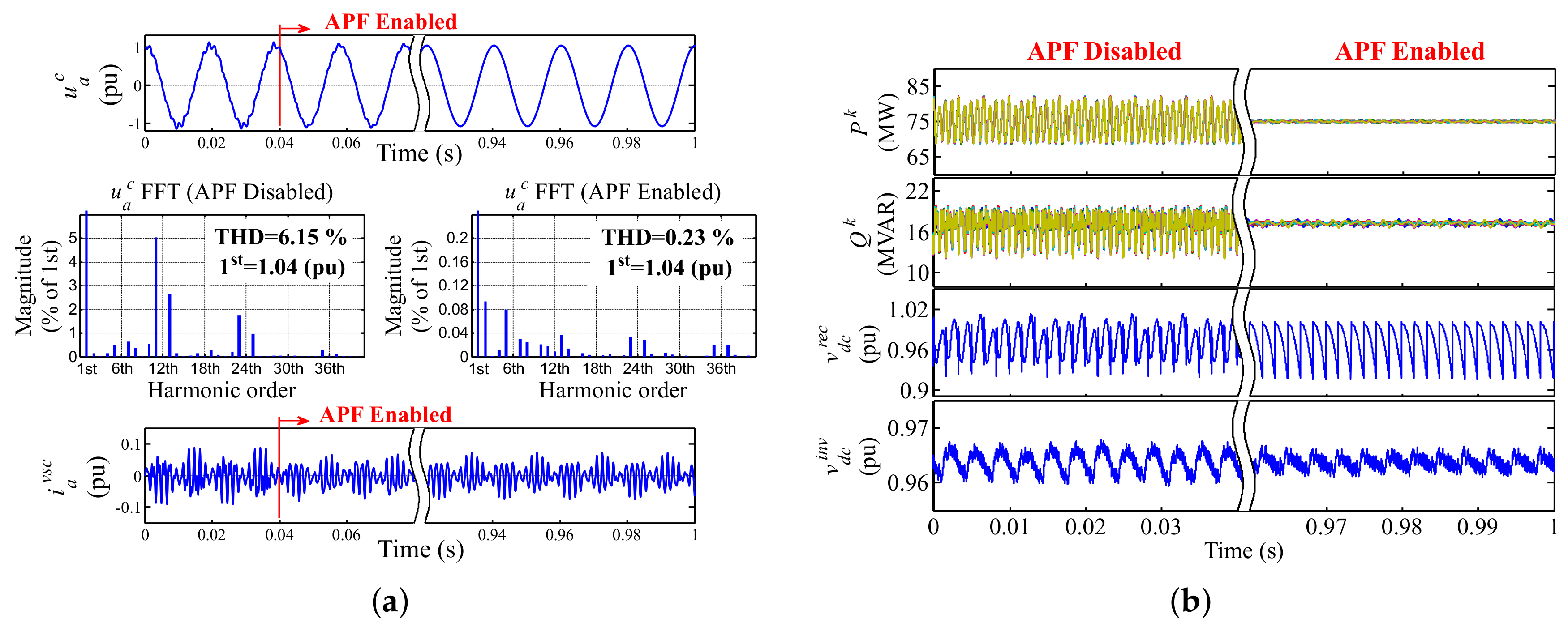
The steady-state performance of the proposed APF has been tested with the OWF operating at the rated power where the considered harmonic currents have their highest values. Figure 8a shows the steady-state response of phase a of the capacitor bank voltage ( u a c ) waveform to the proposed harmonic compensation scheme at the rated power. Initially, the VSC operates only in centralised frequency control mode and harmonic compensation is disabled. During this period, the steady-state waveform of u a c is distorted and its THD is 6.15 %. At t = 0.04 s, the proposed APF is enabled. After a transient, the system returns to the steady-state where u a c has a THD equal to 0.23 %. The APF steady-state response for the waveform of phase a of the VSC current ( i a v s c ) is also represented in Figure 8a. The good transient response to such control variation proves the good stability and capability of the proposed harmonic compensation scheme. It is worth mentioning that the time needed for the APF to achieve the steady-state varies at different operation points, since the harmonic currents values are different at the corresponding operation points.
Moreover, the effect of the proposed harmonic compensation scheme on the WTs’ active and reactive powers as well as the dc-system voltages at the rated power is depicted in Figure 8b. As can be observed, the APF implementation significantly reduces the large ripples of the WTs’ active and reactive powers ( P k and Q k ) created by the harmonic currents of the system. This leads to a power quality improvement in the OWF system which validates the proposed method of APF implementation in such applications. Besides, the rectifier dc-voltage ( v d c r e c ) shows a noticeable harmonic distortion before enabling the APF. These dc harmonic voltages are removed by the proposed control, and as a result, an almost pure 12-pulse per period signal remains for v d c r e c during APF operation. Therefore, enabling the APF also causes a good impact on the HVDC link voltage ripple which is reduced compared to in the APF disabled mode, as can be observed from the onshore inverter dc-voltage ( v d c i n v ) represented in Figure 8b.

6.2. Transient Control Performance

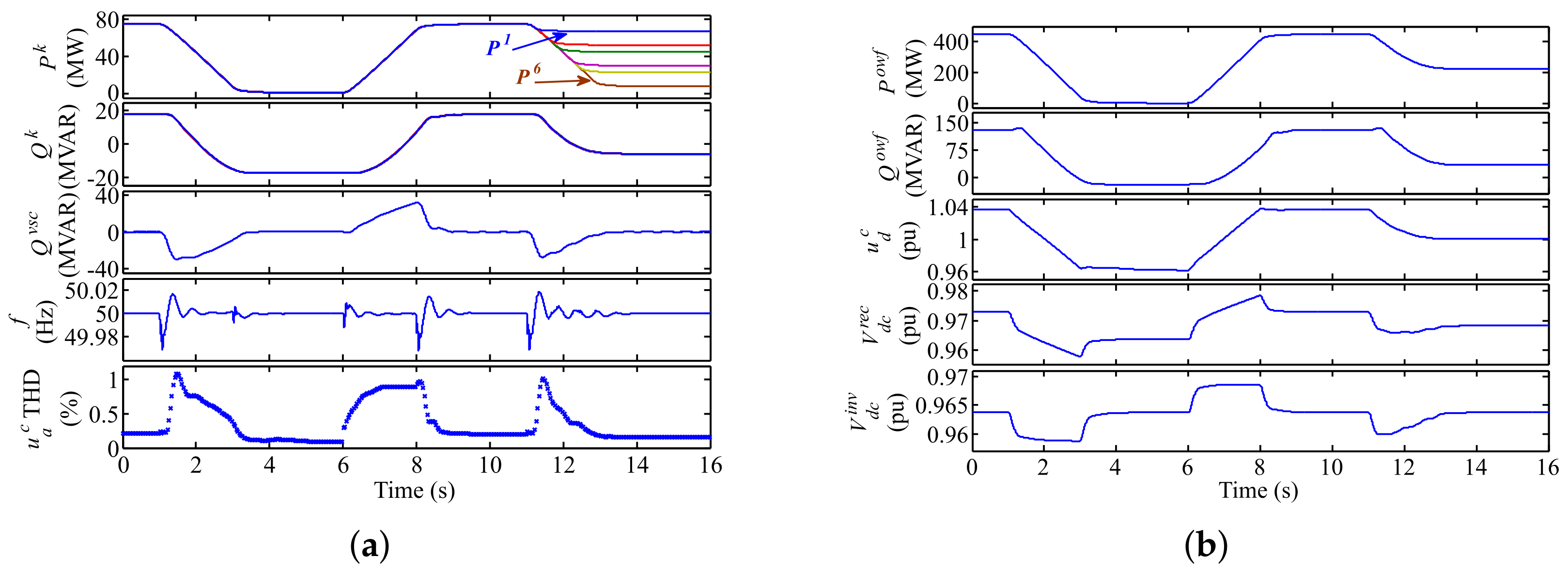
Figure 9 shows the transient performance of the proposed control strategy during scheduled OWF active power changes. Note that, from the beginning, the proposed APF scheme is enabled. Initially, given that the system is in steady-state, the VSC reactive power ( Q v s c ) is zero, and the required steady-state reactive power for the frequency control is provided by the WTs’ reactive powers ( Q k ) thanks to the reactive power command being sent to the WTs. From t = 1 s to t = 3 s, the WTs’ active powers ( P k ) decrease from 100% to 1% of their rated powers. After a transient, Q k reaches a different value as it provides the required steady-state reactive power, while Q v s c returns to zero. Then, from t = 6 s to t = 8 s, P k increases from 1% to 100% of its rated value. After this transient, both Q k and Q v s c return to their initial values. Finally, at t = 11 s, an active power reduction is scheduled. Specifically, the individual WTs’ active powers decrease and reach different values, providing, in total, 50% of the OWF active power. As shown, at steady-state, the same conclusions as before are obtained for both Q k and Q v s c because the reactive power command is sent to the WTs. As can be observed, although the reactive power capability of the WTs is used to provide the required steady-state reactive power, Q v s c varies within approximately ± 8 % of the OWF rated power during the applied transients. As stated before, this variation depends on the OWF active power changes, the communication time delay, and the control and system parameters. This result validates the VSC power rating analysis presented in Section 5. Moreover, the offshore ac-grid frequency (f) is controlled during this scenario with negligible disturbances during the scheduled OWF active power changes. Finally, the THD of phase a of the capacitor bank voltage ( u a c ) is kept below 1% by the proposed harmonic compensation scheme during this scenario.
The aforementioned P k and Q k changes lead to the variation in the active and reactive powers flowing from the OWF to the PCC bus ( P o w f and Q o w f ) which are the result of the offshore ac-grid power flow. According to the corresponding changes in P o w f and Q o w f , the offshore ac-grid voltage magnitude ( u d c ) varies within an acceptable limit of less than ± 4 % of its rated value. As the diode rectifier acts as a voltage clamp on the offshore ac-grid voltage, the average value of the rectifier dc-voltage ( v d c r e c ) has the same trend as u d c with variations of less than ± 2 % of its rated value. However, the average value of the onshore inverter dc-voltage ( v d c i n v ) is regulated at its reference value with negligible variation during the applied transients.

7. Conclusions

This paper presented a novel APF scheme embedded in a centralised frequency control of an OWF connected with a diode-rectifier-based HVDC system. In this scheme, the APF is accomplished by a VSC connected to the rectifier station, which is employed to provide centralised frequency control for the offshore ac-grid. The proposed APF scheme is used to eliminate harmonic currents at a capacitor bank placed at the rectifier station. This results in a significant reduction in the THD of the offshore ac-grid voltage, leading to an improvement in the OWF power quality. Therefore, no passive ac-filter bank is needed at the rectifier station. Also, since no PLL is used, the harmonic current compensation is carried out in the d q reference frame which is independent from any measurement noise and grid disturbance. A new SHC method based on the DP theory is used in the proposed APF scheme which provides the phasor form of harmonics in dc-signals. Then, the well-known PI regulators are used for the harmonic compensation scheme, offering less complexity in terms of the computational requirements compared to the PR regulators. Therefore, the proposed SHC method based on the DP theory could be used instead of any SHC method using a PR controller for APF in both stationary and synchronous reference frames. Moreover, the DP theory is used to obtain the grid solution needed for the system harmonic analysis. Besides, the reactive power capability of the WTs is used to provide the required steady-state reactive power for the frequency control. This is performed by sending the reactive power command to the WTs’ reactive power control channels. Finally, it was demonstrated that the required VSC rated power is reduced. The simulation results validate the performance of the proposal under both steady-state and transient conditions.

Author Contributions

Investigation, A.N.; Methodology, A.N.; Resources, M.Á.C.Á.; Software, A.N. and M.Á.C.Á.; Supervision, J.L.R.A. and S.A.G.; Validation, J.L.R.A. and S.A.G.; Writing–original draft, A.N.; Writing–review and editing, J.L.R.A., S.A.G. and M.Á.C.Á.

Funding

This work was funded by the Autonomous Community of Madrid under the PRICAM project (S2013-ICE-2933).

Conflicts of Interest

The authors declare no conflict of interest.

Appendix A

The ratios for the fundamental magnitude considered for the WTs’ current harmonic injection are shown in Table A1 [22].
Table A1. Harmonic magnitudes of WTs.
Harmonic Order I h / I 1 Harmonic Order I h / I 1
20.343 %220.330 %
40.201 %230.369 %
50.435 %250.235 %
70.471 %260.200 %
80.401 %280.133 %
100.545 %290.271 %
111.456 %310.24 %
131.854 %320 %
140.475 %340 %
160.371 %350.350 %
170.761 %370.259 %
190.420 %380 %
200.324 %400 %

Appendix B

The impedance matrix of the grid at a frequency corresponding to the harmonic order (h) is Z ( h ) . This matrix provides the voltage stationary solution of the grid, using the different current injections as inputs. Matrix M ( h ) is slightly different, because there is a node whose input is changed to voltage and whose output becomes current. Specifically, this is the PCC bus which is placed at position n inside the matrix Z ( h ) . Then, the terms of M ( h ) can be calculated as follows:
m i , j = z i , j z i , n z n , j z n , n i n , j n , m i , j = z n , j z n , n i = n , j n m i , j = z i , n z n , n i n , j = n , m i , j = 1 z n , n i = n , j = n .

Appendix C

The switching functions for the wye- and delta-connected windings of the twelve-pulse diode rectifier ac-currents considering the commutation angle are shown in Equations (A2) and (A3), respectively. By summation of both equations, Equation (16) can be obtained.
S i a , b , c Y / Y 6 P ( t ) = 2 3 π { n = 0 k ( 6 n + 1 ) cos ( 6 n + 1 ) ( ω 0 t μ 2 + γ ) n = 1 k ( 6 n 1 ) cos ( 6 n 1 ) ( ω 0 t μ 2 + γ ) }
where γ equals zero for phase a, 2 π 3 for phase b, and 2 π 3 for phase c; k ( 6 n ± 1 ) = sin ( ( 6 n ± 1 ) μ / 2 ) ( 6 n ± 1 ) 2 μ / 2 ; and μ is the commutation angle of the diodes.
S i a , b , c Y / Δ 6 P ( t ) = 2 3 π { n = 0 D k ( 6 n + 1 ) cos ( 6 n + 1 ) ( ω 0 t μ 2 + γ ) n = 1 D k ( 6 n 1 ) cos ( 6 n 1 ) ( ω 0 t μ 2 + γ ) }
where D = ( 1 ) n .

Appendix D

Following the assumption that there are no harmonic currents in the twelve-pulse rectifier dc side (constant i d c r e c ( t ) = I d c ), the corresponding terms in Equation (19) would be as follows:
I ̲ 1 rec = 4 3 π I d c sin μ / 2 μ / 2 e j ( α + μ / 2 ) , I ̲ ( 12 n + 1 ) rec = 4 3 π I d c k ( 12 n + 1 ) e j ( 12 n + 1 ) ( α + μ / 2 ) I ̲ ( 12 n 1 ) rec = 4 3 π I d c k ( 12 n 1 ) e j ( 12 n 1 ) ( α + μ / 2 )
where k ( 12 n ± 1 ) = sin ( ( 12 n ± 1 ) μ / 2 ) ( 12 n ± 1 ) 2 μ / 2 .

Appendix E

The arbitrary constants of solution Q c f w t ( t ) (A and B) are calculated in a way that satisfies the initial conditions of Q w t ( 0 ) = b c l and d Q w t ( 0 ) d t = 0 (because of the considered time delay). This leads to the following results for the values of A and B.
  • If ( K 4 2 K 5 ) > 0 :
    A = K 4 2 K 5 ( 2 τ K 7 ( ( b c l + K 8 ) ( K 4 + K 4 2 K 5 ) ) ) 2 ( K 4 2 K 5 ) , B = b c l K 8 A ;
  • If ( K 4 2 K 5 ) < 0 :
    A = b c l K 8 , B = K 5 K 4 2 ( 2 τ K 7 b c l K 4 K 8 K 4 ) K 5 K 4 2 ;
  • If ( K 4 2 K 5 ) = 0 :
    A = b c l K 8 , B = 2 τ K 7 b c l K 4 K 4 K 8 2 τ .

Appendix F

Table A2 shows the parameters of the system used in the simulation.
Table A2. System parameters.
DescriptionValueDescriptionValue
S b a s e , a c 450 MVA L f 6.2 mH
V b a s e , a c 220 kV R f 24.2 m Ω
P b a s e , d c 450 MW L s 595.44 mH
V b a s e , d c 594.209 kV R s 2.5 Ω
T r e c x = 0.12 pu  x / r = 80 (66 kV/220 kV) S v s c 0.08 pu
T o w f x = 0.1 pu  x / r = 80 (33 kV/66 kV) V b a s e , d c v s c 100 kV
T w t x = 0.07 pu  x / r = 80 (0.69 kV/33 kV) C d c i n v 0.2 μ F
b c (capacitor bank C)0.05 pu f 0 50 Hz
ac-cable 1.2 km ( π -model)R = 68.4 m Ω L = 0.234 mH C = 3.96 μ F k p 1
ac-cable 2 km ( π -model)R = 67.2 m Ω L = 0.606 mH C = 6.888 μ F k i 5
ac-cable 10 km ( π -model)R = 18.2 m Ω L = 0.34 mH C = 21.11 μ F k r e c 0.23
dc-cable modelaccording to [27] and 200 km x l 0.192 pu
onshore grid equivalentx = 0.05 pu  x / r = 80 v = 1 pu x t 0.12 pu
VSC equivalent dc-capacitance3.33 μ F b c l 0.237 pu
communication time delay0.1 s τ 0.1 s

References

  1. Perveen, R.; Kishor, N.; Mohanty, S.R. Off-shore wind farm development: Present status and challenges. Renew. Sustain. Energy Rev. 2014, 29, 780–792. [Google Scholar] [CrossRef]
  2. Bahrman, M.P.; Johnson, B.K. The ABCs of HVDC transmission technologies. IEEE Power Energy Mag. 2007, 5, 32–44. [Google Scholar] [CrossRef]
  3. Shi, G.; Cai, X.; Sun, C.; Chang, Y.; Yang, R. All-DC offshore wind farm with parallel connection: An overview. In Proceedings of the 12th IET International Conference on AC and DC Power Transmission (ACDC 2016), Beijing, China, 28–29 May 2016. [Google Scholar]
  4. Wei, Q.; Wu, B.; Xu, D.; Zargari, N.R. Medium frequency transformer based configuration for voltage source converter based offshore wind farm. In Proceedings of the 2016 IEEE 8th International Power Electronics and Motion Control Conference (IPEMC-ECCE Asia), Hefei, China, 22–26 May 2016; pp. 3521–3525. [Google Scholar]
  5. Shi, G.; Zhang, J.; Cai, X.; Zhu, M. Decoupling control of series-connected DC wind turbines with energy storage system for offshore DC wind farm. In Proceedings of the 2016 IEEE 7th International Symposium on Power Electronics for Distributed Generation Systems (PEDG), Vancouver, BC, Canada, 27–30 June 2016; pp. 1–6. [Google Scholar]
  6. Menke, P.; Zurowski, R.; Christ, T.; Seman, S.; Giering, G.; Hammer, T.; Zink, W.; Hacker, F.; Imamovic, D.; Thisted, E.; et al. Breakthrough in DC Grid Access Technology for Large Scale Offshore Wind Farms; EWEA Offshore: Copenhagen, Denmark, 2015; pp. 1–5. [Google Scholar]
  7. Saborío-Romano, O.; Bidadfar, A.; Göksu, Ö.; Altin, M.; Cutululis, N.A.; Sørensen, P.E. Connection of OWPPs to HVDC networks using VSCs and Diode Rectifiers: An Overview. In Proceedings of the 15th International Workshop on Large-Scale Integration of Wind Power into Power Systems as Well as on Transmission Networks for Offshore Wind Power Plants, Vienna, Austria, 15–17 November 2016. [Google Scholar]
  8. Blasco-Gimenez, R.; Añó-Villalba, S.; Rodríguez-D’derlée, J.; Morant, F.; Bernal, S. Voltage and frequency control of SG based wind farms with uncontrolled HVDC rectifier. In Proceedings of the 2010 IEEE International Symposium on Industrial Electronics, Bari, Italy, 4–7 July 2010; pp. 2499–2504. [Google Scholar]
  9. Blasco-Gimenez, R.; Ano-Villalba, S.; Rodriguez-D’Derlée, J.; Bernal-Perez, S.; Morant, F. Diode-based HVdc link for the connection of large offshore wind farms. IEEE Trans. Energy Convers. 2011, 26, 615–626. [Google Scholar] [CrossRef]
  10. Blasco-Gimenez, R.; Ano-Villalba, S.; Rodríguez-D’Derlée, J.; Morant, F.; Bernal-Perez, S. Distributed voltage and frequency control of offshore wind farms connected with a diode-based HVdc link. IEEE Trans. Power Electron. 2010, 25, 3095–3105. [Google Scholar] [CrossRef]
  11. Prignitz, C.; Eckel, H.G.; Achenbach, S.; Augsburger, F.; Schön, A. FixReF: A control strategy for offshore wind farms with different wind turbine types and diode rectifier HVDC transmission. In Proceedings of the 2016 IEEE 7th International Symposium on Power Electronics for Distributed Generation Systems (PEDG), Vancouver, BC, Canada, 27–30 June 2016; pp. 1–7. [Google Scholar]
  12. Prignitz, C.; Eckel, H.G.; Achenbach, S. FixReF: A current control strategy for offshore wind turbines connected to different types of hvdc transmission. In Proceedings of the 15th Wind Integration Workshop, Vienna, Austria, 15–17 November 2016; pp. 1–8. [Google Scholar]
  13. Iván, A.A.; Ruben, P.G.; Blasco-Gimenez, R.; Javier, R.A. Control strategy of a HVDC-Diode Rectifier connected type-4 off-shore wind farm. In Proceedings of the Future Energy Electronics Conference (IFEEC), Taipei, Taiwan, 1–4 November 2015; pp. 1–6. [Google Scholar]
  14. Yu, L.; Li, R.; Xu, L. Distributed PLL-based Control of Offshore Wind Turbine Connected with Diode-Rectifier based HVDC Systems. IEEE Trans. Power Deliv. 2017, 33, 1328–1336. [Google Scholar] [CrossRef]
  15. Cardiel-Alvarez, M.A.; Arnaltes, S.; Rodriguez-Amenedo, J.L.; Nami, A. Decentralized Control of Offshore Wind Farms Connected to Diode-based HVDC Links. IEEE Trans. Energy Convers. 2018, 33, 1233–1241. [Google Scholar] [CrossRef]
  16. Von Hofen, M.; Karwatzki, D.; Baruschka, L.; Mertens, A. Hybrid offshore HVDC converter with diode rectifier and Modular Multilevel Converter. In Proceedings of the 2016 IEEE 7th International Symposium on Power Electronics for Distributed Generation Systems (PEDG), Vancouver, BC, Canada, 27–30 June 2016; pp. 1–7. [Google Scholar]
  17. Nguyen, T.H.; Lee, D.C.; Kim, C.K. A series-connected topology of a diode rectifier and a voltage-source converter for an HVDC transmission system. IEEE Trans. Power Electron. 2014, 29, 1579–1584. [Google Scholar] [CrossRef]
  18. Cardiel-Alvarez, M.A.; Rodriguez-Amenedo, J.L.; Arnaltes, S.; Montilla-DJesus, M. Modeling and Control of LCC Rectifiers for Offshore Wind Farms Connected by HVDC Links. Energy Convers. IEEE Trans. 2017, 32, 1284–1296. [Google Scholar] [CrossRef]
  19. Baldi, S.; Papachristodoulou, A.; Kosmatopoulos, E.B. Adaptive pulse width modulation design for power converters based on affine switched systems. Nonlinear Anal. Hybrid Syst. 2018, 30, 306–322. [Google Scholar] [CrossRef]
  20. Blasco-Gimenez, R.; Aparicio, N.; Ano-Villalba, S.; Bernal-Perez, S. LCC-HVDC connection of offshore wind farms with reduced filter banks. IEEE Trans. Ind. Electron. 2013, 60, 2372–2380. [Google Scholar] [CrossRef] [Green Version]
  21. Nguyen, T.H.; Le, Q.A.; Lee, D.C. A novel HVDC-link based on hybrid voltage-source converters. In Proceedings of the Energy Conversion Congress and Exposition (ECCE), Montreal, QC, Canada, 20–24 September 2015; pp. 3338–3343. [Google Scholar]
  22. Mendonça, G.; Pereira, H.; Silva, S. Wind farm and system modelling evaluation in harmonic propagation studies. In Proceedings of the International Conference on Renewable Energies and Power Quality (ICREPQ’12), Santiago de Compostela, Spain, 28–30 March 2012; pp. 28–30. [Google Scholar]
  23. Limongi, L.; Bojoi, I.R.; Griva, G.B.; Tenconi, A. Digital current-control schemes. IEEE Ind. Electron. Mag. 2009, 3, 20–31. [Google Scholar] [CrossRef] [Green Version]
  24. Lascu, C.; Asiminoaei, L.; Boldea, I.; Blaabjerg, F. High performance current controller for selective harmonic compensation in active power filters. IEEE Trans. Power Electron. 2007, 22, 1826–1835. [Google Scholar] [CrossRef]
  25. Daryabak, M.; Filizadeh, S.; Jatskevich, J.; Davoudi, A.; Saeedifard, M.; Sood, V.; Martinez, J.; Aliprantis, D.; Cano, J.; Mehrizi-Sani, A. Modeling of LCC-HVDC systems using dynamic phasors. IEEE Trans. Power Deliv. 2014, 29, 1989–1998. [Google Scholar] [CrossRef]
  26. Filatrella, G.; Nielsen, A.H.; Pedersen, N.F. Analysis of a power grid using a Kuramoto-like model. Eur. Phys. J. B 2008, 61, 485–491. [Google Scholar] [CrossRef] [Green Version]
  27. Abouzlam, M.; Ouvrard, R.; Poinot, T.; Benchaib, A. Identification of a HVDC cable model with coupling between core and screen. IFAC-PapersOnLine 2015, 48, 1433–1438. [Google Scholar] [CrossRef]
  28. Sun, Y.; Zhang, G.; Xu, W.; Mayordomo, J.G. A harmonically coupled admittance matrix model for AC/DC converters. IEEE Trans. Power Syst. 2007, 22, 1574–1582. [Google Scholar] [CrossRef]
  29. Li, S.; Xu, L.; Haskew, T.A. Control of VSC-based STATCOM using conventional and direct-current vector control strategies. Int. J. Electr. Power Energy Syst. 2013, 45, 175–186. [Google Scholar] [CrossRef]
  30. Szechtman, M.; Wess, T.; Thio, C. A benchmark model for HVDC system studies. In Proceedings of the International Conference on AC and DC Power Transmission, London, UK, 17–20 September 1991; pp. 374–378. [Google Scholar]
Figure 1. System under study: (a) The considered offshore wind farm (OWF); (b) system simplified model.
Energies 11 02718 g001
Figure 2. Extraction of the capacitor bank’s harmonic voltage vectors.
Energies 11 02718 g002
Figure 3. Overall system control loops.
Energies 11 02718 g003
Figure 4. Centralised frequency control: (a) vector diagram in the stationary and the synchronous reference frames; (b) the frequency control (FC) scheme; (c) wind turbines’ (WTs’) reactive power reference control.
Energies 11 02718 g004
Figure 5. Harmonic compensation (HC): (a) the HC scheme; (b) the selective harmonic compensation (SHC) diagram.
Energies 11 02718 g005
Figure 6. Voltage source converter (VSC) power rating analysis: (a) simplification of the considered OWF for the VSC power rating analysis; (b) wind turbine (WT) reactive power control scheme.
Energies 11 02718 g006
Figure 7. WT active power and dynamic responses of the WT and the VSC reactive powers in the VSC power rating analysis.
Energies 11 02718 g007
Figure 8. Steady-state active power filtering (APF) performance at the rated power: (a) phase a of the capacitor bank voltage and its fast Fourier transform (FFT) spectrum, and phase a of the VSC current; (b) the WTs’ active and reactive powers, rectifier dc-voltage, and onshore inverter dc-voltage.
Energies 11 02718 g008
Figure 9. Transient control performance during the OWF active power changes: (a) WTs’ active and reactive powers, VSC reactive power, offshore ac-grid frequency and total harmonic distortion (THD) of phase a of the capacitor bank voltage; (b) OWF active and reactive powers, capacitor bank voltage magnitude, and the average values of the rectifier and onshore inverter dc-voltages.
Energies 11 02718 g009