1. Introduction
Winter icing of transmission lines is one of the natural disasters of the power system. The rare long-term freezing disaster in early 2008 caused serious damage to the power grid in southern China, resulting in a large number of tower collapses, line interruptions, substation outages, and so on, which caused huge losses in many southern provinces of China.
For transmission line icing, manual deicing or improving line anti-icing designs were the main methods up until recently, but efficiency was low or investment was high. In order to cope with the impact of more and more frequent ice disasters on power system facilities, research into various ice-melting technologies has been receiving more and more attention [
1,
2,
3,
4,
5].
Among them, DC current ice-melting has the advantages of high efficiency, a wide ice-melting range for different transmission lines, and small power supply. A previous study [
6] proposes a diode-based uncontrolled rectifier DC ice-melting device, which only has the function of ice melting, and which is only used during the covering-ice period of transmission lines in winter. However, it has low utilization rate, and consumes system reactive power when ice-melting, which affects voltage stability. Another study [
7] proposes a Static Var Compensator (SVC) type DC ice-melting device, which can run in two modes: DC ice-melting or SVC reactive power compensation. However, the ice-melting and reactive power compensation cannot run at the same time and it cannot meet the reactive demand of ice melting. Further more, the harmonics of ice-melting are large, and a huge filter device is needed. Further studies [
8,
9,
10,
11,
12] propose a new modular multi-level DC ice-melting device, which combines the dynamic reactive power compensation capability of a chain Static Var Generator (SVG) with the four-quadrant operation capability of a half-bridge modular multi-level converter (MMC). It can output DC voltage at the same time to meet the DC ice-melting demand, but the reactive power compensation and DC ice-melting need to be designed in the same capacity. The cost is high, and it is still in the theoretical research stage.
In view of the above problems associated with the ice-melting device, this paper proposes a low-harmonic DC ice-melting device that can compensate for simultaneous reactive power when ice melting. The harmonics injected into the power grid are small without a filtering device when ice melting. The device itself achieves a reactive power balance ensuring grid voltage stability. The paper is organized as follows:
Firstly, the topology of the low-harmonic DC ice-melting device with simultaneous reactive power compensation is proposed. The SVG and the ice-melting rectifier share the ice-melting transformer, which eliminates the SVG’s connection reactance and reduces the SVG’s output voltage and the insulation design. The design enables simultaneous operation of ice melting and reactive power compensation.
Secondly, the output voltage ripple characteristics of the low-harmonic DC ice-melting device is analyzed. The 12-pulse rectification structure is adopted, and the ripple factor value is only 0.994, which effectively reduces the output DC current fluctuation.
Thirdly, using the Fourier series, the harmonics injected into the power grid are mainly 5th and 7th harmonic currents when ice-melting. Increasing the number of power modules and the triangular carrier frequency can effectively eliminate the SVG’s lower harmonic.
Fourthly, injecting low-order harmonic multi-carrier phase-shift modulation algorithm which injects 5th and 7th harmonics into a modulated wave is put forward. Using the simultaneous operation of ice melting and reactive power compensation, the algorithm can eliminate the harmonic injected into the grid when ice melting.
Finally, the simulation and experimental research on the low-harmonic DC ice-melting device which was built in the 500 kV Chuanshan substation is carried out. The results verify that DC ice-melting has low-harmonic characteristics and that the reactive power compensation function can effectively improve grid voltage stability.
2. Low-Harmonic DC Ice-Melting Device Structure
2.1. Overall Topology
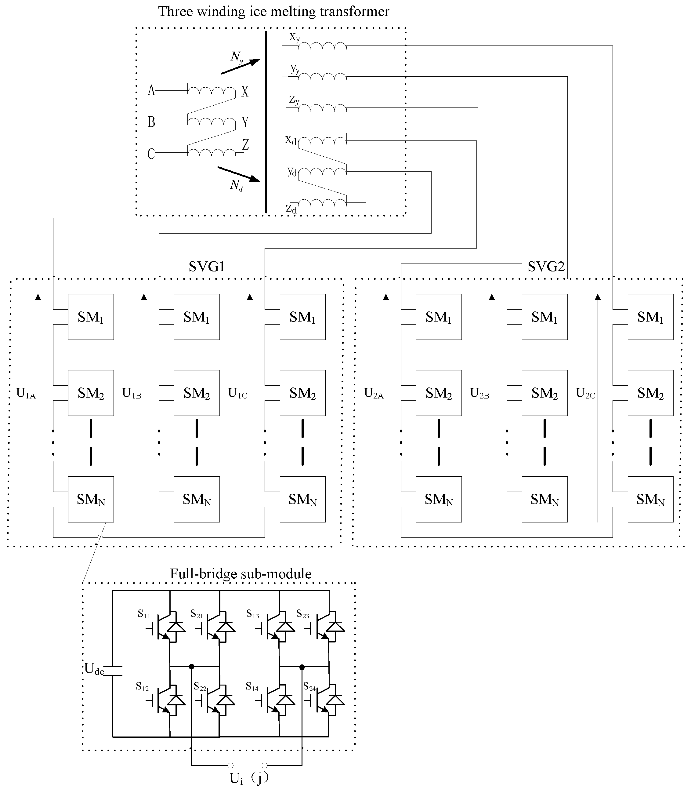
The structure of the low-harmonic DC ice-melting device capable of simultaneous reactive power compensation is shown in
Figure 1. It is mainly composed of an ice-melting transformer, SVG1, SVG2, Rectifier1, Rectifier2, and Isolation switch. SVG1 and SVG2 are connected to the two low-voltage winding sides of the transformer which can effectively reduce the SVG’s output voltage. The SVG can absorb harmonics generated on the input side when the rectifier is running.
The SVG and the transformer realize dynamic reactive power compensation. The SVG can provide fast and flexible dynamic reactive power for the power grid, support the grid voltage especially when ice-melting, and improve the stability and power quality of the power system [
13,
14,
15]. In the structure shown in
Figure 1, the leakage reactance of the transformer is used as a connection reactance to replace the special reactor connected to the SVG and the grid, reducing the land occupation and cost of the SVG. The low-harmonic DC ice-melting device has the characteristics of optimized configuration of ice-melting capacity and reactive power compensation capacity. The capacity of each component of the ice-melting device can be configured according to the ice-melting and dynamic reactive power requirements of the substation avoiding the excessive design of the ice-melting or reactive capacity [
16].
The topology shown in
Figure 1 can make full use of the transformer, providing dynamic reactive power support for the grid system during daily operation. The SVG can also eliminate harmonics and reactive power generated by the rectifier during the ice-melting operation mode.
2.2. SVG Structure
The SVG structure of the low-harmonic DC ice-melting device is shown in
Figure 2. The SVG1 and SVG2 are connected to the triangular and star-shaped windings of the transformer’s sub-edge without special connection reactance which is replaced by the transformer’s leakage reactance.
In order to meet the requirements of the connection between SVG and power grid, the value of the transformer leakage reactance range is 8–13%. The calculation formula is as shown in Equation (1):
where
f—Frequency (Hz);
I—Rated current (A);
W—Coil number (Turn);
et—Every potential (V);
H—Average reactance height of two coils (m); Σ
D—Magnetic flux leakage area (m
2); ρ—Rockwell coefficient;
K—Additional reactance coefficient, generally take 1.
The SVG’s output voltage is connected to the grid after being boosted by the transformer, which reduces the SVG’s insulation voltage design difficulty [
17,
18], reduces the number of each phase power modules connected in series, and simplifies the design of the control system. In order to improve the reactive output current and meet the demand for large-capacity reactive power compensation above 100 MVar, the SVG’s power modules adopt dual IGBT (Insulated Gate Bipolar Transistor) parallel structure. The parallel IGBT adopts the same control pulses.
3. Output Characteristics of Low-Harmonic DC Ice-Melting Device
3.1. Output Voltage Ripple Characteristicsof Rectifier
The low-harmonic DC ice-melting device uses two 6-pulse rectifier bridges in series or parallel configuration. Each 6-pulse rectifier bridge consists of several diodes, damping absorption resistors, and capacitors. The number of series diodes in each bridge arm is proportional to the input voltage. The two 6-pulse rectifier bridges realize series or parallel 12-pulse DC voltage output through the switch
K1,
K2, and
K3. The output DC voltage is as shown in Equation (2):
In Equation (2), m is the number of DC voltage pulse waves output from the rectifier. U2L is the RMS (Root Meam Square) value of the AC voltage which is input to the rectifier.
The output voltage of the 12-pulse rectifier is as shown in Equation (3) where
U2 is the RMS value of the input AC voltage of the rectifier.
Perform Fourier series decomposition on Equation (3):
where
k = 1, 2, 3….
Ud0 takes the form:
bn takes the form:
The voltage ripple factor γ
u is the ratio of the effective value of the harmonic component of the output DC voltage
ud0 to the average value
Ud0 of the rectified voltage, namely:
In Equation (7)
UR is equal:
where
U is equal:
According to the Equations (4)–(9) we can get the following:
The ripple factor values of the output voltages of different pulse wave rectifiers obtained by Equation (10) are shown in
Table 1.
It can be seen from
Table 1, the more the pulse wave number of the rectifier, the smaller the output voltage ripple value. The 12-pulse rectification structure of the ice-melting device can greatly reduce the voltage ripple factor value and reduce the fluctuation of the output DC current, which is useful to facilitate line ice-melting.
3.2. Output Harmonic Characteristics of Ice-Melting
In Figure1, since the inductance component of the impedance
Zd of the ice-transmission line is very large, the waveform of the DC output current is basically straight, and the input currents of the upper and lower 6-pulse rectifier bridges are rectangular waves, as shown in
Figure 3. It is shown that each phase is turned on by 120°, and the current phases of the corresponding phases of the upper and lower bridges are different by 30°, and the amplitude is
Id/2.
The input currents of the two sets of 6-pulse rectifier bridges are decomposed by Fourier series, and the input current expressions of the two rectifier bridges are respectively:
It can be obtained from Equations (11) and (12): the number of harmonics on the AC side of the rectifier of the low-harmonic DC ice-melting device is 5, 7, 11, …, 6
k ± 1 times,
k = 1, 2, 3, …. The RMS of the fundamental current and each harmonic are:
The RMS value of each harmonic is inversely proportional to the harmonic order. The ratio of the RMS value to the fundamental value is the reciprocal of the harmonic order. The higher the harmonic order, the smaller the harmonic amplitude, so the harmonics injected into the grid during the ice-melting are mainly the 5th and 7th harmonic currents, which are 0.156Id and 0.111Id, respectively.
3.3. Output Harmonic Characteristics of Reactive Power Compensation
In
Figure 1, the number of cascaded power modules per phase is
N in SVG1 and SVG2. In order to increase the reactive output current, each power module adopts a dual IGBT parallel structure, and the output phase voltage is Fourier-decomposed:
where
Udc is the power module DC bus voltage,
m is the modulation degree,
ω is the sinusoidal modulation wave angle frequency,
ωc is the carrier triangle wave angular frequency, and
θk (
k = 1, 2, …,
N) is the power module carrier phase-shifted angle.
When n is an odd number, .
When n is even, take the carrier ratio: .
fc is the triangular carrier frequency and
f is the sinusoidal modulation wave frequency.
where
Jn is an n-time Bessel function.
According to Bessel’s Equation (15), Equation (14) can be expressed as:
among them:
In the Equation (17),
θk (
k = 1, 2, …,
N) is a carrier phase-shifted angle. When the carrier phase-shifted PWM (Pulse Width Modulation) technique is adopted, the carrier angle of each power module is sequentially increased by
π/
N. It is not difficult to prove “
B = 0” because “
n = 2, 4, 6,
…” and “
A = 0” when “
n < 2
N”. It can be seen that the output voltage
Uug/
Udc will no longer contain “2
Nkc ± 1” or less harmonics. Therefore, as the number
N of cascaded power modules per phase increases and the triangular carrier frequency
fc increases, the low harmonics of SVG1 and SVG2 can be effectively eliminated [
19,
20,
21].
4. Injection Low-Order Harmonic Multi-Carrier Phase-Shifted Modulation Algorithm
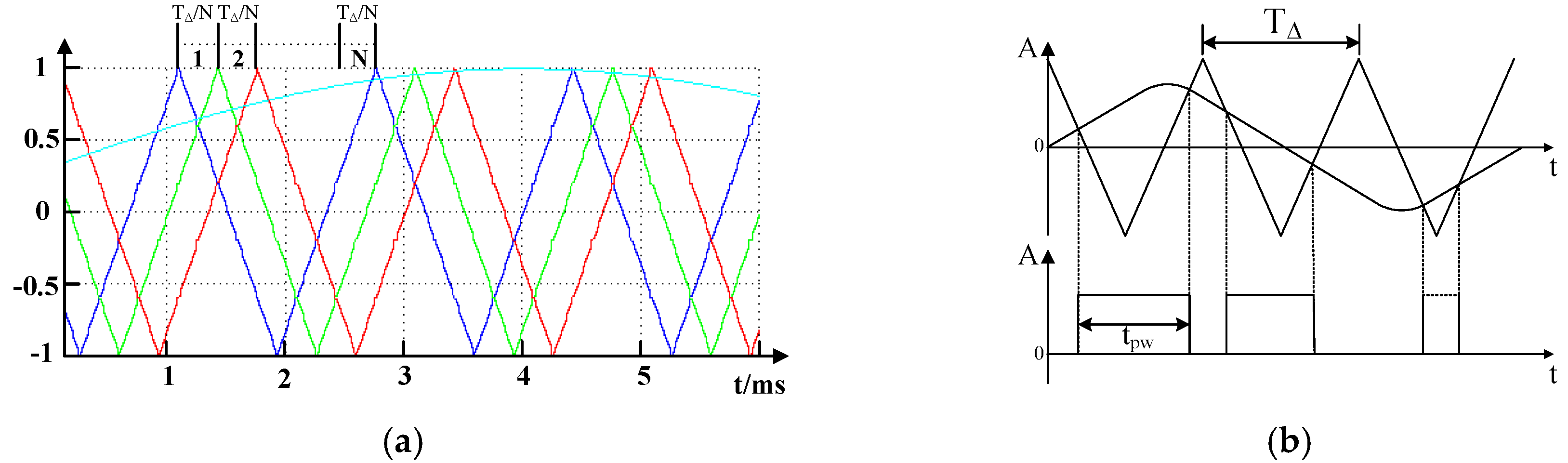
In high-power equipment, the switching frequency of power electronics devices is so low that good control performance can’t be obtained with a single converter. In order to overcome this problem, multi-carrier phase-shifted modulation algorithms were researched. A multi-carrier phase-shifted modulation algorithm is the combination of the multi-modular technique and SPWM (Sine Pulse Width Modulation) technique. The high equivalent switching frequency can be obtained with low switching frequency devices. This technique improves the equivalent switching frequency through the counteraction of lower order harmonics though not simply through processing the harmonic from lower order to higher order to get a perfectly performing harmonic feature with no filter. The American Robincon Company first invented the technology and applied for a patent (P.W.Hammond. Medium voltage PWM drive and method. U.S. Patent 5 625 545, April 1997).
In the multi-carrier phase-shifted modulation algorithm of the SVG with cascaded power module, the DC voltage utilization of the in-phase modulation algorithm is the highest, and the practical application is the most extensive. When the in-phase modulation algorithm is used, the modulation waves of the left and right bridge arms of each power module in
Figure 2 are for:
The control method of each power module with three-phase AC input and the single-phase AC output adopts a sinusoidal pulse width modulation method. The power modules of the same phase have the same carrier frequency, but the phases are sequentially different by 1/
N carrier period, as shown in
Figure 4a.
The pulse calculation method of each power module adopting sinusoidal pulse width modulation methodis shown in
Figure 4b.
The formula for calculating the pulse width is:
where
TΔ is the period of the triangular carrier,
m1 is the modulation ratio of the sine wave and the triangular wave.
In each power module of
Figure 2, the power devices IGBT S
11 and S
21 are connected in parallel, S
12 and S
22 are connected in parallel, S
13 and S
23 are connected in parallel, and S
14 and S
24 are connected in parallel. The two parallel IGBT pulse control signals are the same, and the power module upper and lower arms S
11 and S
12, S
13, and S
14 pulse control signals are complementary. In order to avoid solving complex transcendental equations, the power switching device pulse control signal is obtained by using the regular sampling method. The calculation principle is shown in
Figure 5a.
In
Figure 5a,
θi is the angle value of the midpoint sampling time of the triangular wave.
The calculation results of Equations (20) and (21) are the offset time between the start and stop times of each pulse control signal of S11 in the power module and the corresponding triangle wave midpoint.
The calculation results of Equations (22) and (23) are the offset time between the start and stop times of each pulse control signal of S13 in the power module and the corresponding triangle wave midpoint.
In order to eliminate the 5th and 7thharmonic currents injected into the grid during the ice-melting [
22,
23,
24], the 5th and 7th harmonic voltages are modulated into the power module modulation wave of SVG1 and SVG2. The harmonic amplitudes are
k1 and
k2, respectively, so that the generated harmonic current is equal to the amplitude of the harmonic current injected into grid when ice-melting, and the direction is opposite. After the 5th and 7th harmonic voltages are injected into the modulated wave of the left and right bridge arms of each power module, the waveform of the modulated wave is as shown in
Figure 6. The calculation formulas of the modulated wave of the left and right bridge arms are as shown in Equation (24):
According to Equations (14)–(17) and (24), after the 5th and 7th harmonics are injected, the phase voltages of each phase of SVG1 and SVG2 are:
where
k1 and
k2 are obtained by detecting the 5th and 7th harmonic currents injected into the grid by the ice-melting rectifier and performing Fourier decomposition.
The principle of IGBT control pulse generation in each power module of the SVG is shown in
Figure 7 [
25,
26,
27,
28,
29].
5. Simulation and Test Results
The 500 kV Chuanshan substation is located in Hengyang City, Hunan Province, China. It is an important hub substation in southern Hunan Province. In Hunan Power Grid’s extremely large ice disaster in 2008, several lines of the Chuanshan substation were in a state of suspension, the icing of each line was serious, and a large area of the inverted tower and broken line appeared. The parameters of icing lines in the Chuanshan substation are shown in
Table 2.
At the 500 kV voltage level of Hunan Power Grid, it can be found that the area with low voltage transient instability is concentrated in the south of the Hunan Province. The local voltage distribution map of southern Hunan is enlarged as
Figure 8. A low voltage problem in a steady state and a voltage instability problem in the disturbed state exist in the southern Power Grid of Hunan Province. With high-speed rail, electric irons, and other impact loads, the dynamic reactive power demand is large in the Chuanshan substation. Therefore, it is necessary to install a dynamic reactive power compensation device of a certain capacity in southern Hunan.
Combined with the demand for ice-melting of the lines in the Chuanshan substation and the dynamic reactive demand in southern Hunan, a low-harmonic DC ice-melting device with simultaneous reactive power compensation was installed in the Chuanshan substation to solve the problem of dynamic reactive power and line ice-melting at the same time. The ice-melting capacity is 120 MW, and the reactive power compensation capacity of SVG1 and SVG2 are all 50 MVar. The ice-melting transformer has a rated capacity of 120 MVA, a rated input voltage of 35 kV, a rated output voltage of 17.1 kV, and a short-circuit impedance of 15%. The ice-melting rectifier has a rated capacity of 120 MW, a rated output DC voltage of 21 kV, and a rated output DC current of 5700 A. SVG1 and SVG2 have a rated output voltage of 17.1 kV and a rated output current of 1688 A. The number of power modules per phase is 20, which is half the number of power modules compared with the 35 kV grid-connected without a transformer. This greatly improves the stability of the SVG.
5.1. Simulation Results
Using PSCAD (Power System Computer Aided Design)/EMTDC (Electro Magnetic Transient in DC System) simulation software, the ice-melting and dynamic reactive power compensation characteristics of the low-harmonic DC ice-melting device installed in the 500 kV Chuanshan substation were simulated. The transformer was connected with the 35 kV low voltage system bus in the substation. The simulation results of each function are describing in following subsections:
5.1.1. DC Ice-Melting
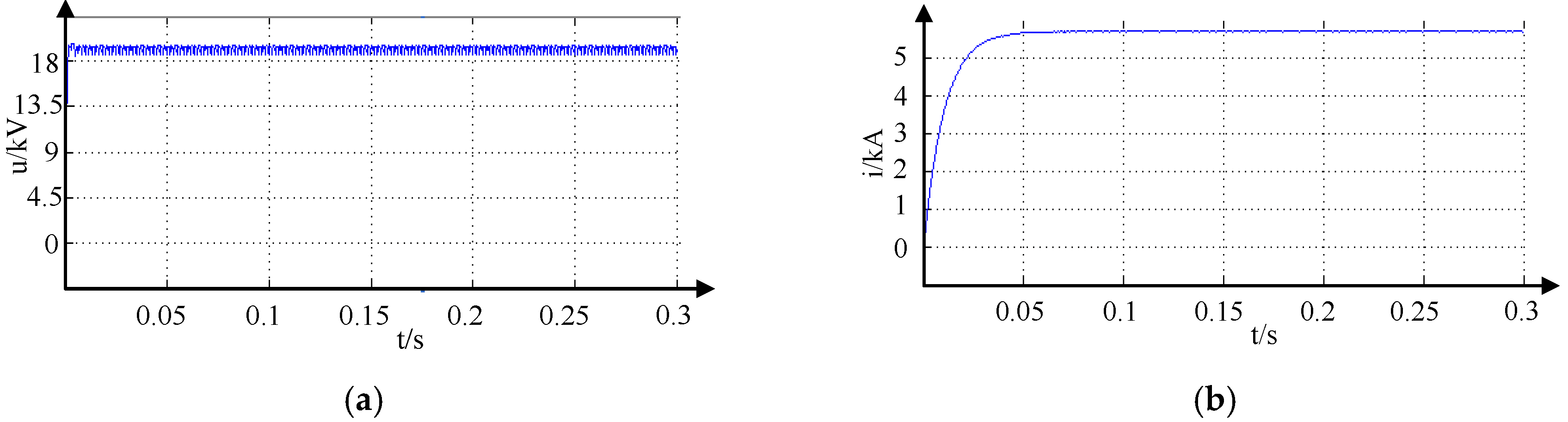
Taking the DC ice-melting of the 500 kV Chuangu line as an example, its DC resistance per phase was 1.88 Ω, the line length was 130.3 km, and the wire type was 2 × LGJ–500. When ice melting, the A phase and C phase are connected in a series, the output voltage of the ice-melting transformer is 17.1 kV, and the 12-pulse rectifier is connected in parallel by two bridges. During the simulation, it was possible to obtain an output DC voltage of the ice-melting device of 18.9 kV, an output DC current of 5685 A, and the voltage and current waveforms are shown in
Figure 9a,b. The ripple factor value of the output voltage is small in
Figure 9a and the output current waveform is smooth in
Figure 9b. The actual output is consistent with the previous theoretical analysis.
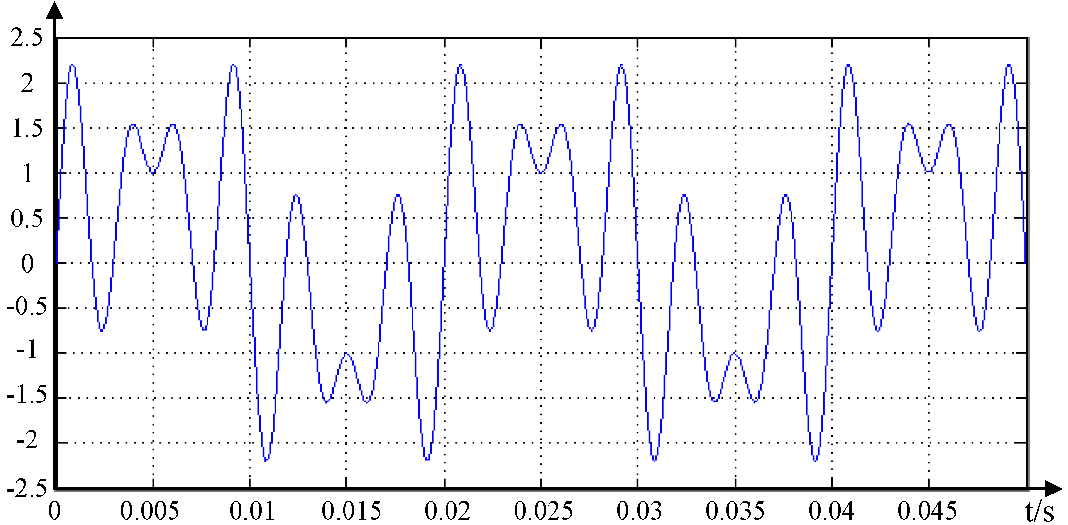
Figure 10 is a low-order harmonic simulation analysis of the current waveform of the input side of the ice-melting rectifier when ice-melting. When the rectifier is working, it will generate large 5th and 7th harmonics on its input side, but it can be seen from
Figure 5 that the 5th and 7th harmonics in the input current are effectively eliminated by the SVG1 and SVG2 connected in parallel to the input side of the rectifier, and the content is less than 0.5%.
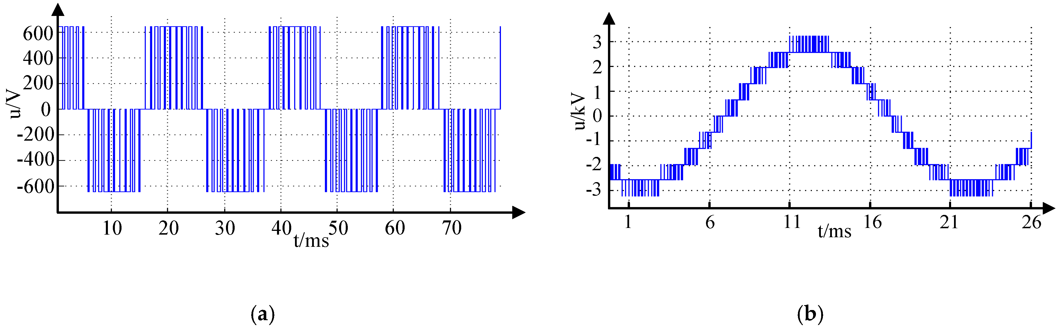
5.1.2. Output Voltage Waveform of SVG
In order to reduce the amount of calculations for the controller, the carrier frequency is generally taken as an integral multiple of the fundamental frequency. The single power module’s carrier frequency is 350 Hz and the output voltage is about 494 V in SVG1 and SVG2. The output three-level voltage waveform of the single power module is as shown in
Figure 11a.
Arbitrarily selecting five power modules connected in the A phase of SVG1 or SVG2 to simulate, the output of the eleven-level voltage waveform is as shown in
Figure 11b. The output level of SVG is equal to “2
n + 1” where n is the number of power module per phase,
n = 1, 2, 3.....
5.1.3. SVG Compensation 35 kV System Reactive
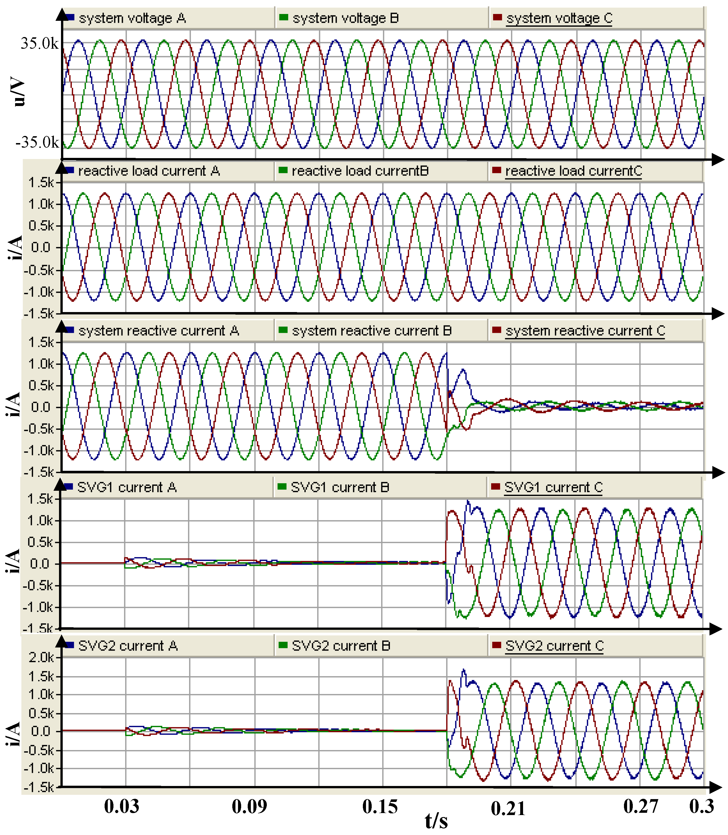
If the capacitive reactive demand of the 35 kV system in the substation is 60 MVar, the reactive current in the system can be fully compensated when the SVG is put into operation at 0.2 s. Each SVG outputs reactive power 30 MVar. The system voltage, reactive load current, system reactive current, SVG1 output current, and SVG2 output current are shown in
Figure 12. As can be seen from the figure, the SVG can effectively compensate the reactive load current to maintain the voltage stability of the 35 kV system voltage.
5.2. Test Results
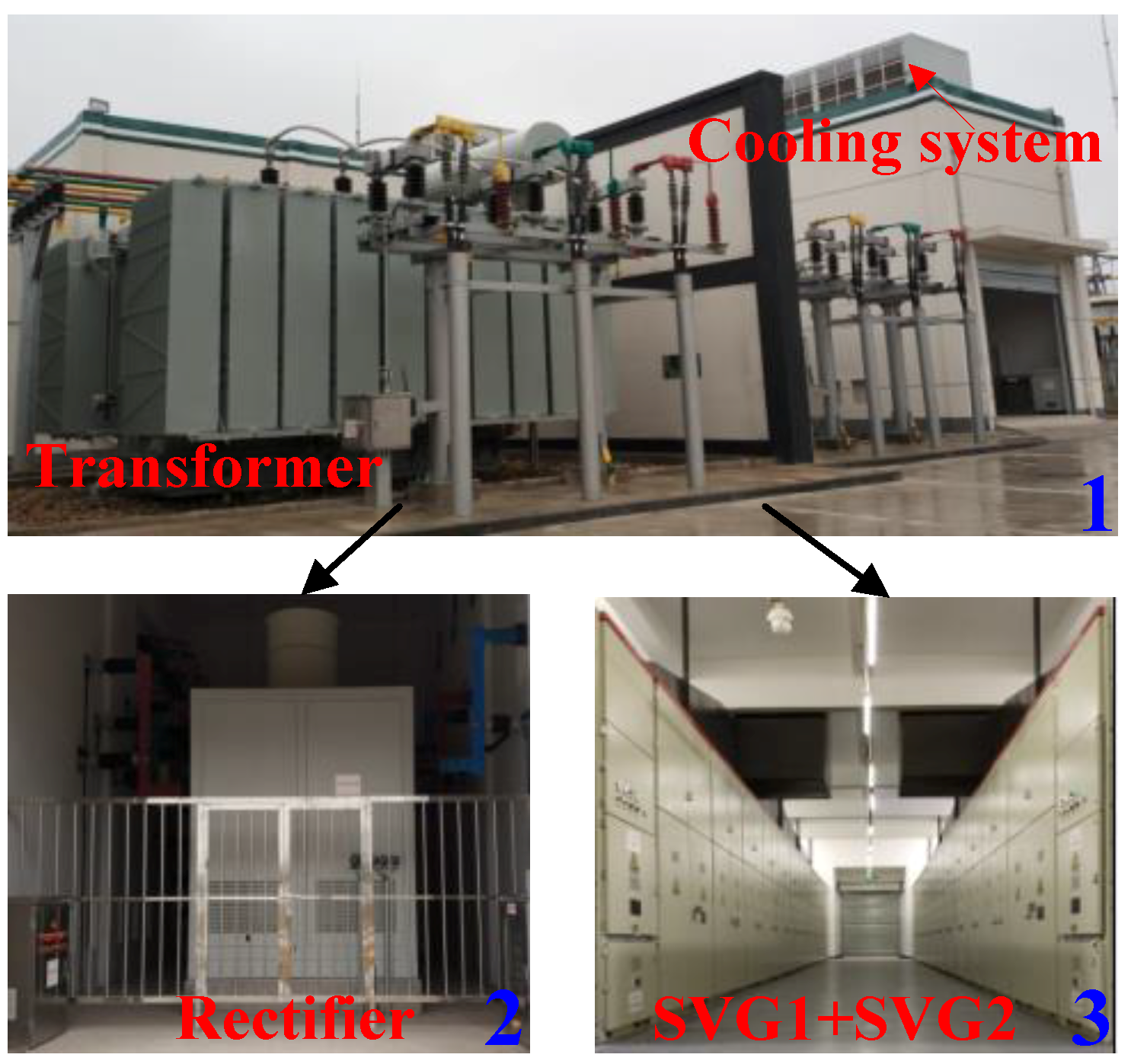
The low-harmonic DC ice-melting device of the 500 kV Chuanshan substation with simultaneous reactive power compensation is shown in
Figure 13. It consists of a transformer, a rectifier, SVG1, SVG2, and a cooling system.
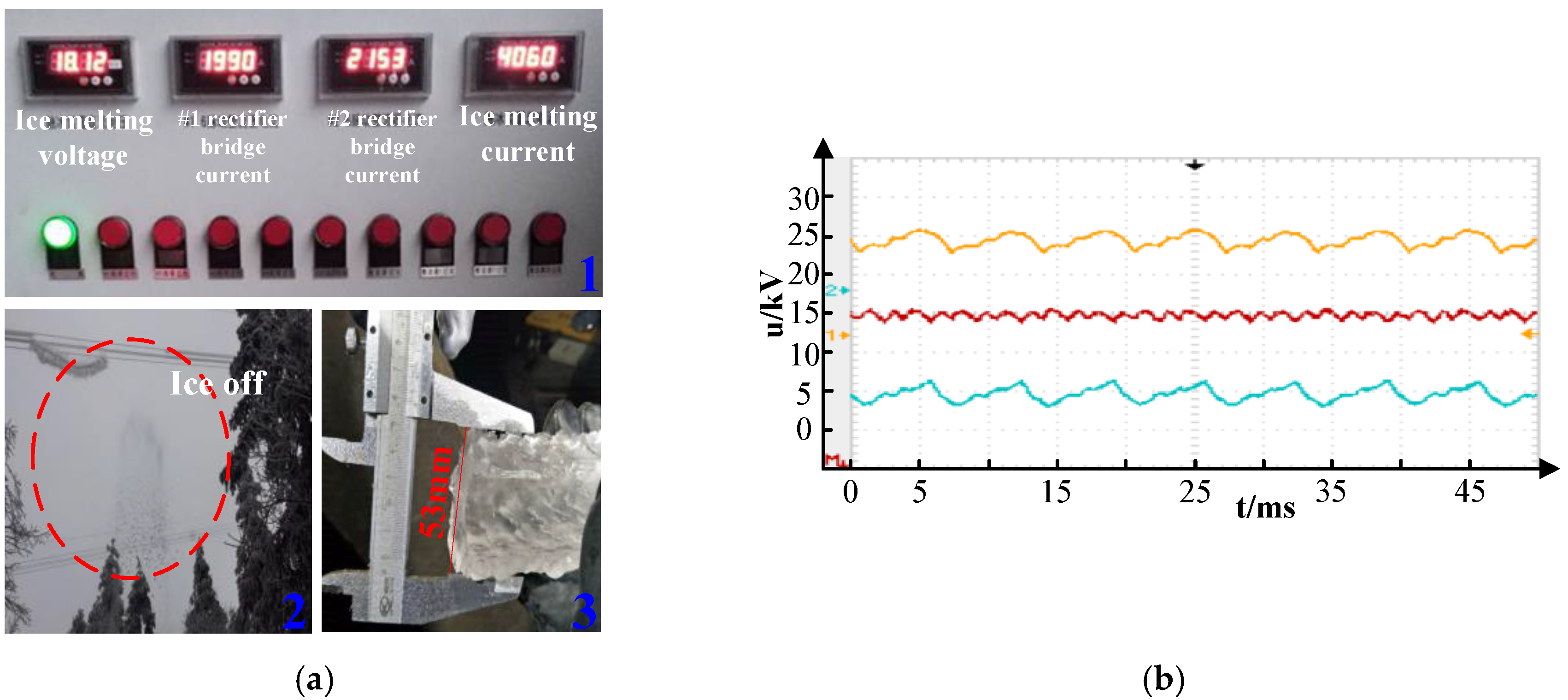
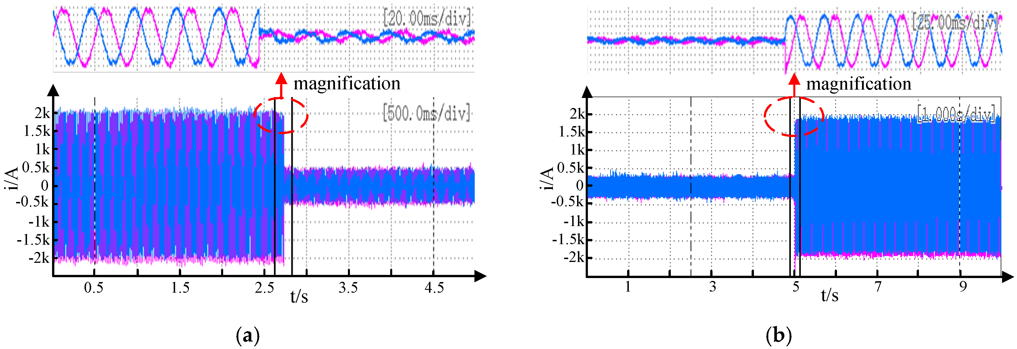
On 28 January 2018, the 500 kV Chuansu I line had ice as thick as 50 mm. There was a risk of an inverted tower and broken line. The low-harmonic DC ice-melting device was used to melt the ice on lines. The output voltage of the transformer was 17.1 kV. The 12-pulse rectifier adopted two bridges in parallel. The DC ice-melting current was 4060 A, and the ice-melting voltage was 18.12 kV. First, the A and C phases were melted in series for about 35 min, and then the B and C phases were melted in series which took about 33 min to melt the ice. The output voltage, current and line falling ice is as shown in
Figure 14a when ice-melting.
The output voltage of the ice-melting is shown in
Figure 14b. The voltage ripple number is 12 in each cycle, and the output voltage ripple value is about 0.99, which is consistent with the theoretical calculation. When ice-melting, SVG1 and SVG2 run in parallel with the injected low-harmonic multi-carrier phase-shift modulation algorithm. The 5th and 7th harmonic currents injected into the grid by the rectifier are effectively eliminated as shown in
Figure 15.
The single power module’s carrier frequency is 300 Hz in SVG1 and SVG2, the output voltage is about 482 V. The output three-level voltage waveform of each power module is as shown in
Figure 16a. The SVG’s A phase output voltage waveform is as shown in
Figure 16b.The actual test results are consistent with the previous simulation results.
When the inductive reactive power requirement of the substation’s power system is reduced from 80 MVar to 20 MVar, the single SVG output reactive power is reduced from 40 MVar to 10 MVar. The output current waveforms of the A and C phase are shown in
Figure 17a. When the system inductive reactive power requirement is increased from 20 MVar to 80 MVar, the single SVG output reactive power is increased from 10 MVar to 40 MVar, and the A and C phase output current waveforms are as shown in
Figure 17b.
When the reactive power requirement of the power system changes from 80 MVar sensibility to −80 MVar capacitive, the single SVG output reactive power is changed from 40 MVar to −40 MVar, and the A and C phase output current waveforms are shown in
Figure 18.
The SVG output reactive response time is less than 10 ms which can well meet the reactive power demand of power system according to the
Figure 17 and
Figure 18.
After the low-harmonic DC ice-melting device in Chuanshan substation was put into operation, the power quality of Chuanshan substation was tested for 24 h using the power quality tester according to the test procedures. The 500 kV bus voltage had no negative deviation, and the positive deviation of 500 kV bus voltage was about 0.80–2.0% within 24 h of testing, as shown in
Figure 19. The ninety-five percent probability of the positive deviation value (phase B) was about 1.57%, which was 1.52% lower than the 3.09% when there was no timely reactive power compensation at runtime.
So the low-harmonic DC ice-melting device capable of simultaneous reactive power compensation can effectively improve the voltage stability in southern Hunan Province.
6. Discussion
The simulated and measured results in
Section 5 can be explained as follows:
The topology of a low-harmonic DC ice-melting device capable of simultaneous reactive power compensation is feasible. The SVG uses transformer leakage reactance instead of connecting reactance. It can realize the simultaneous operation of ice-melting and reactive power compensation. The running harmonics are small, and no filtering device is needed.
The twelve-pulse rectification structure in the low-harmonic DC ice-melting device can effectively reduce the fluctuation of output DC current and the ripple factor value is only 0.994.
The ice-melting and SVG reactive power compensation are simultaneously operated, and the injected low-harmonic multi-carrier phase-shift modulation algorithm can effectively eliminate the 5th and 7th harmonics mainly generated during ice melting without the need of a filter device.
After the SVG was put into operation in 500 kV Chuanshan substation, the 500 kV bus voltage had no negative deviation and the positive deviation decreased from 3.09% to 1.57% within 24 h of testing, which effectively improves the voltage stability in southern Hunan Province, China.
7. Conclusions
In this paper, a topology of a low-harmonic DC ice-melting device capable of simultaneous reactive power compensation has been proposed. The ice-melting device is mainly composed of a transformer, SVG1, SVG2, and an ice-melting rectifier. The two SVGs are connected to the two low-voltage winding sides of the transformer, which is also connected to the rectifier. The SVG can effectively absorb harmonics generated by the rectifier and improve the voltage stability.
The simulation and experimental research is carried out. The results verify the feasibility and effectiveness of the low-harmonic DC ice-melting device which provides an effective method for the research and development of the DC ice-melting device.


