1. Introduction
Recently, there has been growing interest in renewable energy because of the depletion of natural resources and increasing environmental pollution from the use of fossil fuels and nuclear energy [
1,
2,
3]. For these reasons, the use of grid-connected inverter systems for renewable energy sources has become an important topic [
4,
5]. High efficiency is required for the effective use of power conditioning systems (PCSs).
Many studies have been conducted to achieve high inverter efficiency. To obtain high efficiency, there are several methods, such as the use of topologies with higher efficiency, highly efficient devices, and modified pulse width modulation (PWM) techniques.
To increase the efficiency of the PCS, highly efficient topologies utilizing the zero-voltage switching (ZVS) techniques have been studied [
6,
7]. These topologies have advantages regarding the efficiency. However, to achieve the ZVS, the required auxiliary circuit and control method are complicated.
Research has been conducted to compare the performance of the Si-IGBT and SiC-MOSFET power devices [
8,
9]. Recently, the SiC-MOSFET has been used widely in inverter systems to achieve higher efficiency, because these high-efficient devices have the advantage of high-speed switching and low switching losses when compared with the Si-IGBT [
10]. However, the efficiency increase by the device has limitation on the performance of the device. SiC-MOSFET is also more expensive than the Si-IGBT.
The modification of the PWM method is the easiest to increase efficiency. The continuous PWM (CPWM) and discontinuous PWM (DPWM) are widely used switching methods for the inverter control [
5,
11]. The Space Vector PWM (SVM) is a typical CPWM. The modulation signal of the SVM is continuously changed depending on the line frequency. On the other hand, the modulation signal of the DPWM is discontinuously changed. The DPWM can be applied based on the sinusoidal PWM (SPWM). The modulation signal is generated by injecting the DPWM offset to the modulation signal of the SPWM. The switching loss of the devices is affected, depending on the switching method. The DPWM can reduce the switching loss because the switching device is not switched when the modulation signal is clamped to the DC-bus. Therefore, the DPWM can increase the efficiency of the inverter.
The Output voltage of the inverter has a lot of harmonics because of the discontinuous change, which depends on the switching states. To control the grid current sinusoidal waveform, the grid-connected filter is essentially required. The aim of this filter is to attenuate the harmonic components in the switching frequency band. Recently, in order to reduce the volume and the cost of the filter, an LC- or LCL-filter (one or two inductors and a capacitor that is connected in parallel per phase) is widely used instead of the L-filter. When using the LC- or the LCL-filter, the resonance frequency band is formed [
12,
13]. In the DPWM, many harmonic voltages are generated in the wide frequency range at the output terminal of the inverter. If these harmonic voltages are in the resonance frequency band, the grid current oscillates [
14]. This problem adversely affects the quality of the current and increases the total harmonic distortion (THD).
The selective harmonic elimination PWM method has been conducted to reduce the harmonic voltage [
15,
16,
17]. This method can minimize the switching loss, while reducing the desired harmonics. Once harmonics, which should be reduced, are determined, switching angles are also determined. In this case, unselected harmonics cannot be reduced. If harmonics in the resonance frequency band are selected, the oscillation problem of the grid current can be solved. However, the resonance frequency is affected by the grid impedance in grid-connected system [
18]. Therefore, if the grid impedance is large, then the harmonics in the resonance frequency band cannot be reduced.
This paper proposes the improved DPWM method to solve the resonance problem. The proposed method injects the sixth harmonic to the modulation signal to reduce the harmonic voltages at the output terminal of the inverter. The attenuation of the harmonics in the resonance frequency band improves the quality of the output current. The proposed algorithm is verified by PSIM simulations and experiments using a 3-kW neutral-point clamped (NPC)-type grid-connected inverter system.
2. Description of Grid-Connected Inverter System
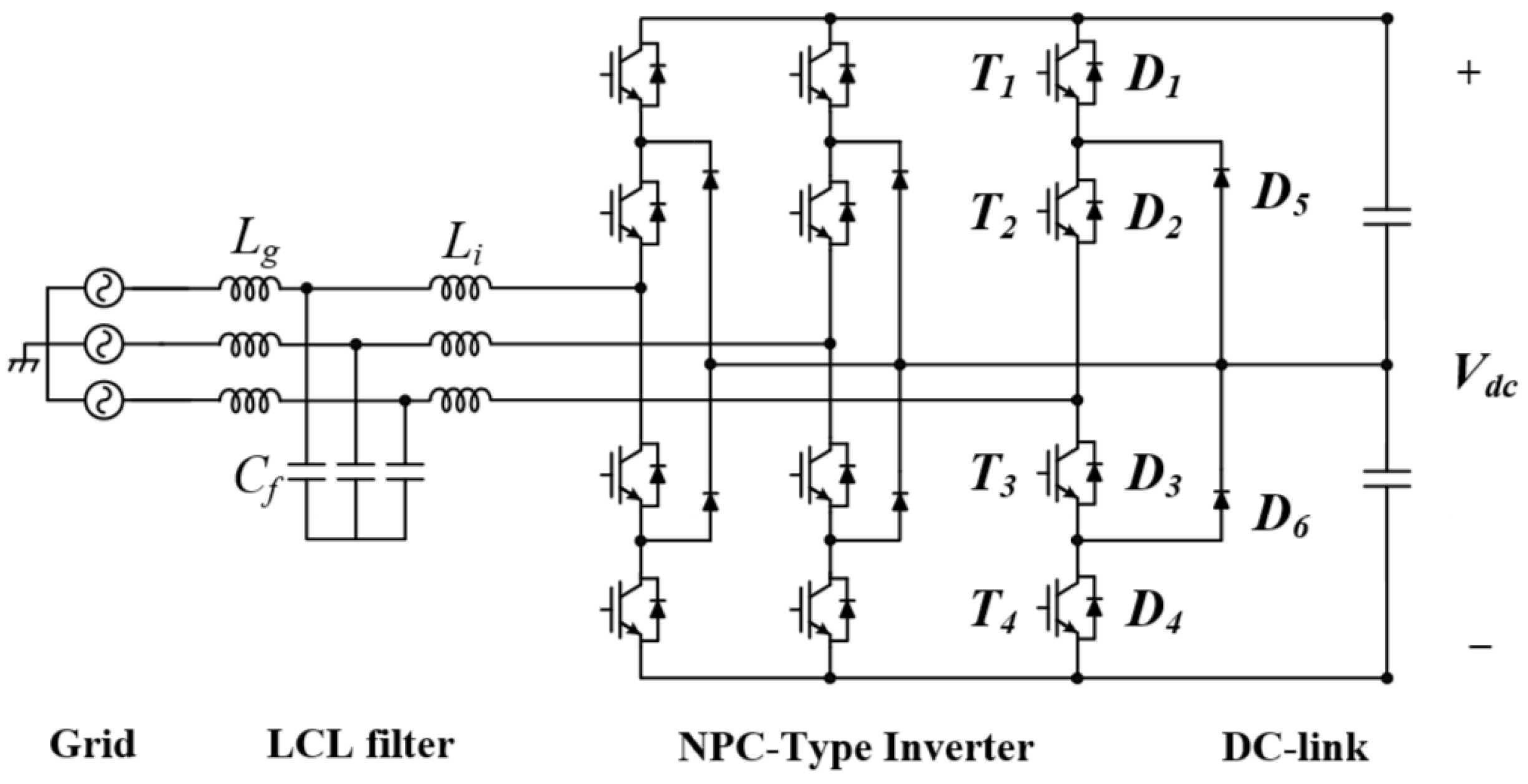
Figure 1 shows the construction of the grid-connected inverter system. This system is composed of an LCL-filter, NPC-type inverter, and DC-link. To transfer the power between the grid and the DC-link, the inverter controls the DC-link and the output current. To reduce the switching ripple of the current, the LCL-filter is used in this paper. The LCL-filter is typically used to reduce the size of the filter. The LCL-filter consists of two inductors and a capacitor that is connected in parallel per phase, as shown in
Figure 1. In this case, the resonance frequency band is formed around the resonance frequency [
16]. The resonance frequency is defined as
where
Li is the inverter side inductor,
Lg is the grid side inductor, and
Cf is the filter capacitor.
The transfer function of the LCL-filter is represented as
where
z2LC = 1/
LTCf,
ω2res =
LTz2LC/
Li, and
LT =
Li +
L2.
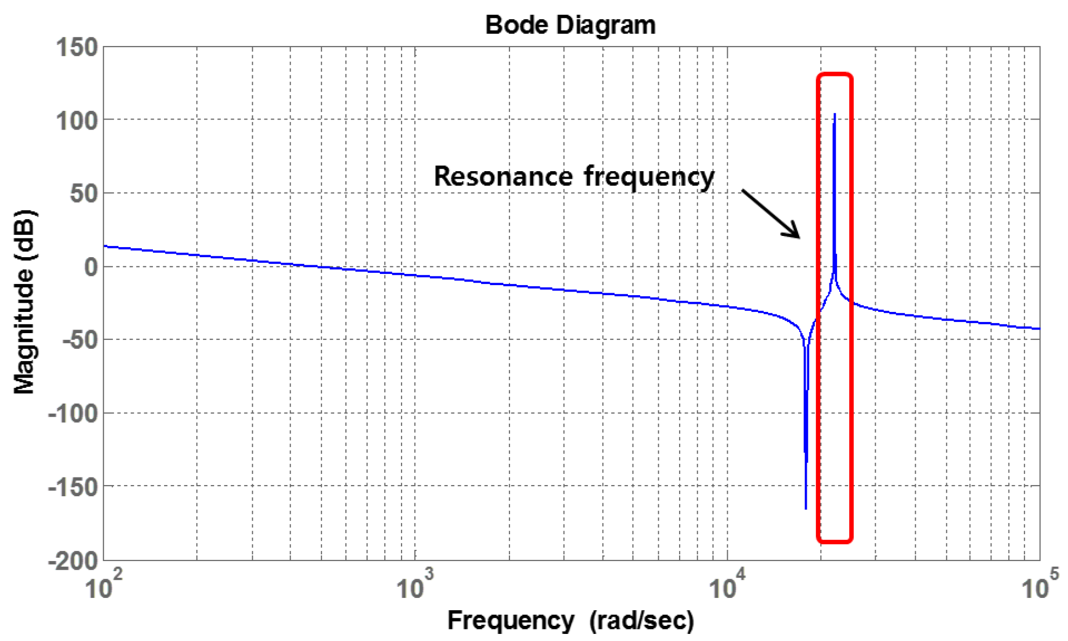
Figure 2 shows a Bode plot of the LCL-filter voltage and current. The LCL-filter parameters are the same as in the simulation condition. The magnitude of the LCL-filter gain is high at the resonance frequency.
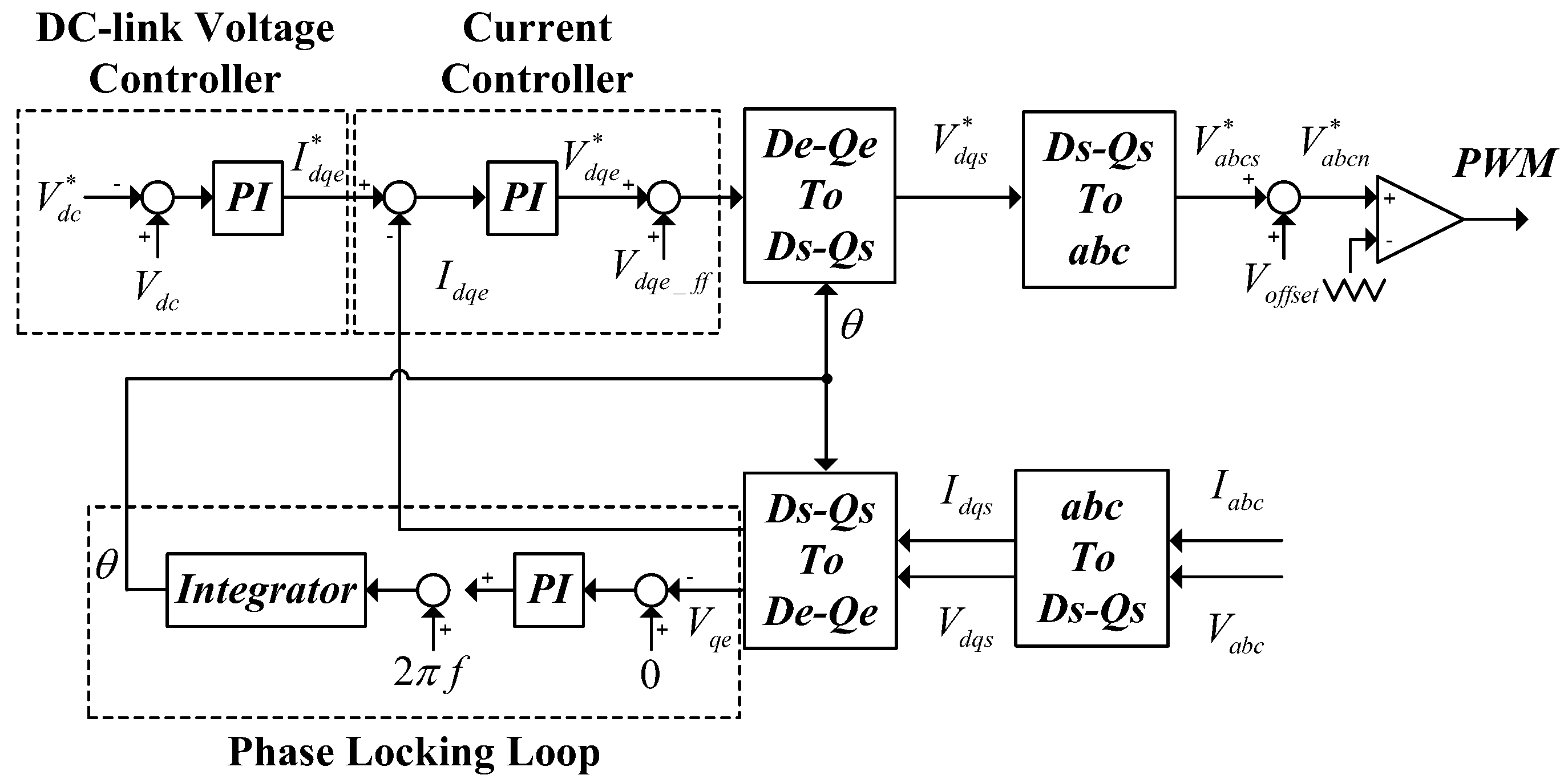
Figure 3 shows the control block of the grid-connected inverter. The dual loop control method is used to regulate the DC-link voltage in this paper. Outer loop is the DC-link controller and the inner loop is the current controller. The output of the outer loop is the reference of the active current for following the DC-link voltage reference. The inner loop can control the active and reactive components, respectively. The inverter that is used in this paper controls the power factor (PF) to 1. The inner loop is performed on the synchronous frame. The output of the inner loop is the dq-axis reference voltage (
V*dqe).
V*dqe changed to phase voltage reference (
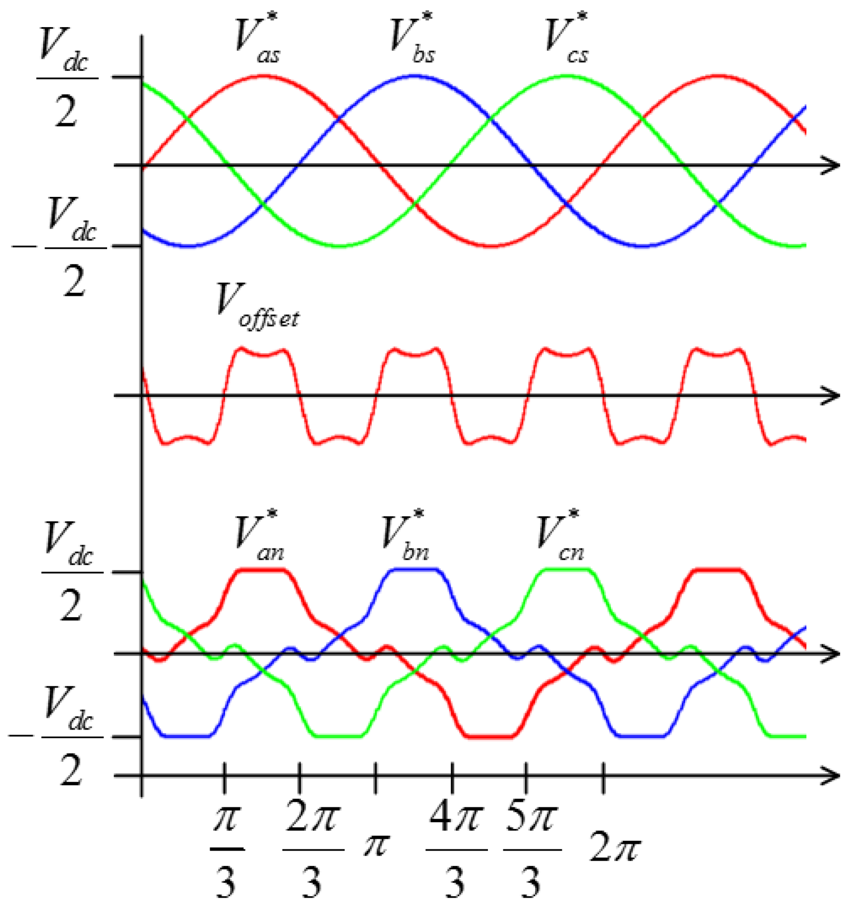
V*abcs) by inverse coordinate transformation. The phase angle used in inverse coordinate transformation is estimated by the phase locked loop (PLL). In grid-connected system, PLL follows the angle of the grid voltage. Therefore,
V*abcs is synchronized with the grid voltage. 60° DPWM is implemented by the offset voltage with microprocessor. The offset voltage is calculated by maximum and minimum of
V*abcs, as shown in Equation (4). The range where the maximum value among
V*abcs is larger than the minimum value among
V*abcs is 60°. In the opposite case, this range is 60°. Therefore, it is possible to implement 60° DPWM, according to the change of the offset voltage. The reference of the pole voltage is the sum of the reference of the phase voltage and the offset voltage. The PWM signal is generated by comparing the carrier signal and the pole voltage reference, which is the sum of the phase voltage reference and the offset voltage.
3. Description of the Conventional 60° DPWM
In the DPWM, there are ranges where the switching devices maintain ON or OFF state. In these ranges, it is possible to reduce the switching loss of the switching devices because of the reduction of the switching amount. Therefore, the DPWM has the merit to increase the efficiency of the inverter by the reduction of the switching loss. In the grid-connected inverter systems, 60° DPWM are widely used among the several DPWM switching methods.
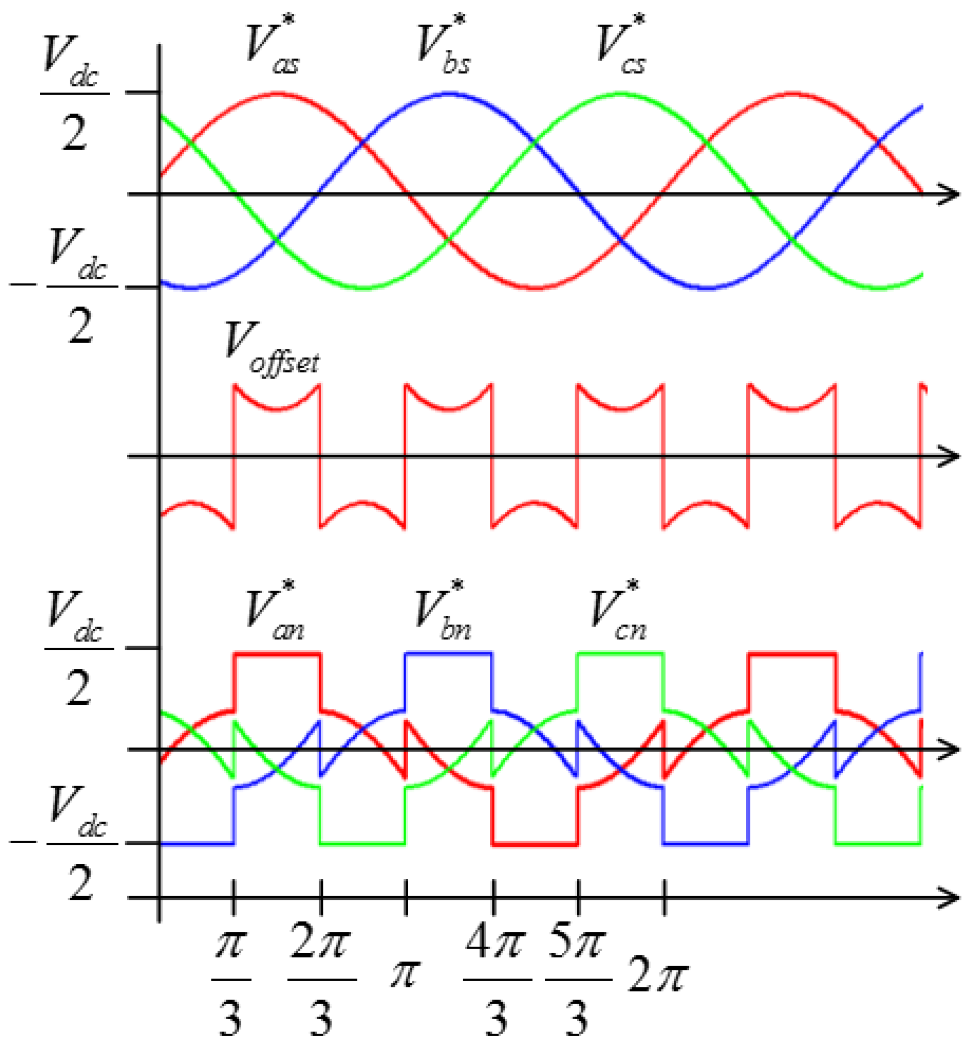
Figure 4 shows the reference and the offset voltage of the 60° DPWM. The pole voltage reference is used in the modulation signal and can be obtained by the sum of the phase voltage reference and the offset voltage. In this method, the switches of one-phase among three-phase maintain ON or OFF state every 60° range. The phase voltage references are used to determine the discontinuous range by comparing the amplitude of each phase voltage reference. These phase voltage reference (
V*as,
V*bs,
V*cs =
V*xs) are expressed as
where
Vm is the amplitude of the phase voltage reference and
ω is the radian representation of 60 Hz fundamental frequency.
The offset voltage is obtained by the maximum and the minimum values of the
V*xs. The offset voltage is expressed as
where
Vmax is the maximum value and
Vmin is the minimum value among the
V*xs and
Vdc is the DC-link voltage.
The pole voltage reference can be obtained by the summation of
V*xs and the
Voffset. The references of the pole voltages (
V*an,
V*bn,
V*cn =
V*xn) are expressed as
4. Analysis of the Resonance Problem with DPWM
In case of the DPWM switching method, V*xn are discontinuously changed because of the discontinuous variation of the offset voltage every 60° range. The output terminals of the inverter are clamped to the DC-bus, according to V*xn. Many harmonics at the output terminals are generated in the wide frequency range at the clamping moments of V*xn. If these harmonics are formed up to the resonance frequency band, harmonic voltages and resonance frequency band overlap. In this case, the grid currents oscillate at the clamping moment of V*xn.
In this paper, to analyze the output voltage harmonics, a numerical method is applied. When using this method, the harmonics can be approximated relatively easily.
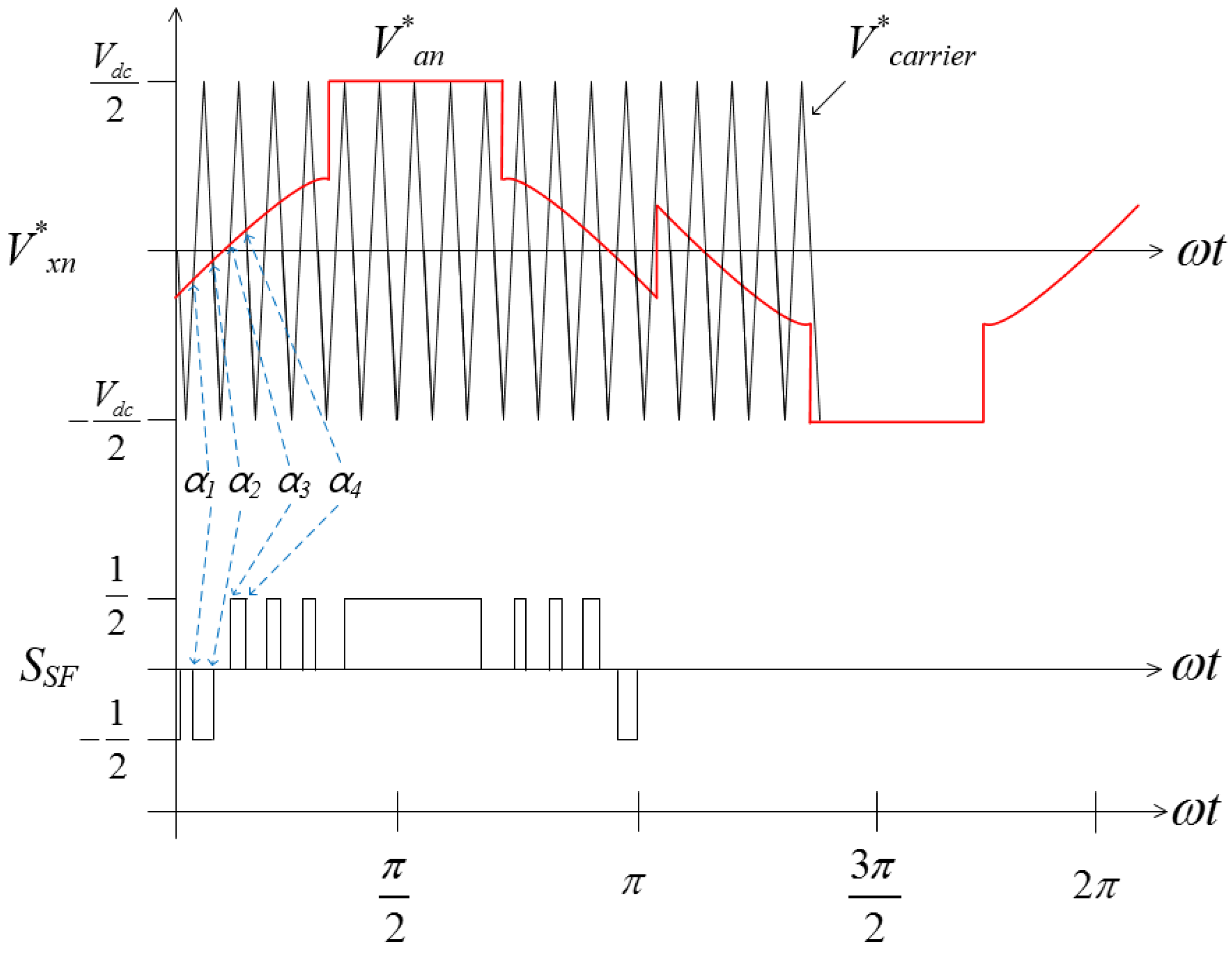
Figure 5 shows the
V*an, carrier signal (
Vcarrier) and the switching function
SSF. The aim of applying the numerical method is to obtain the pattern of the
SSF to analyze the harmonic components of the inverter output voltage.
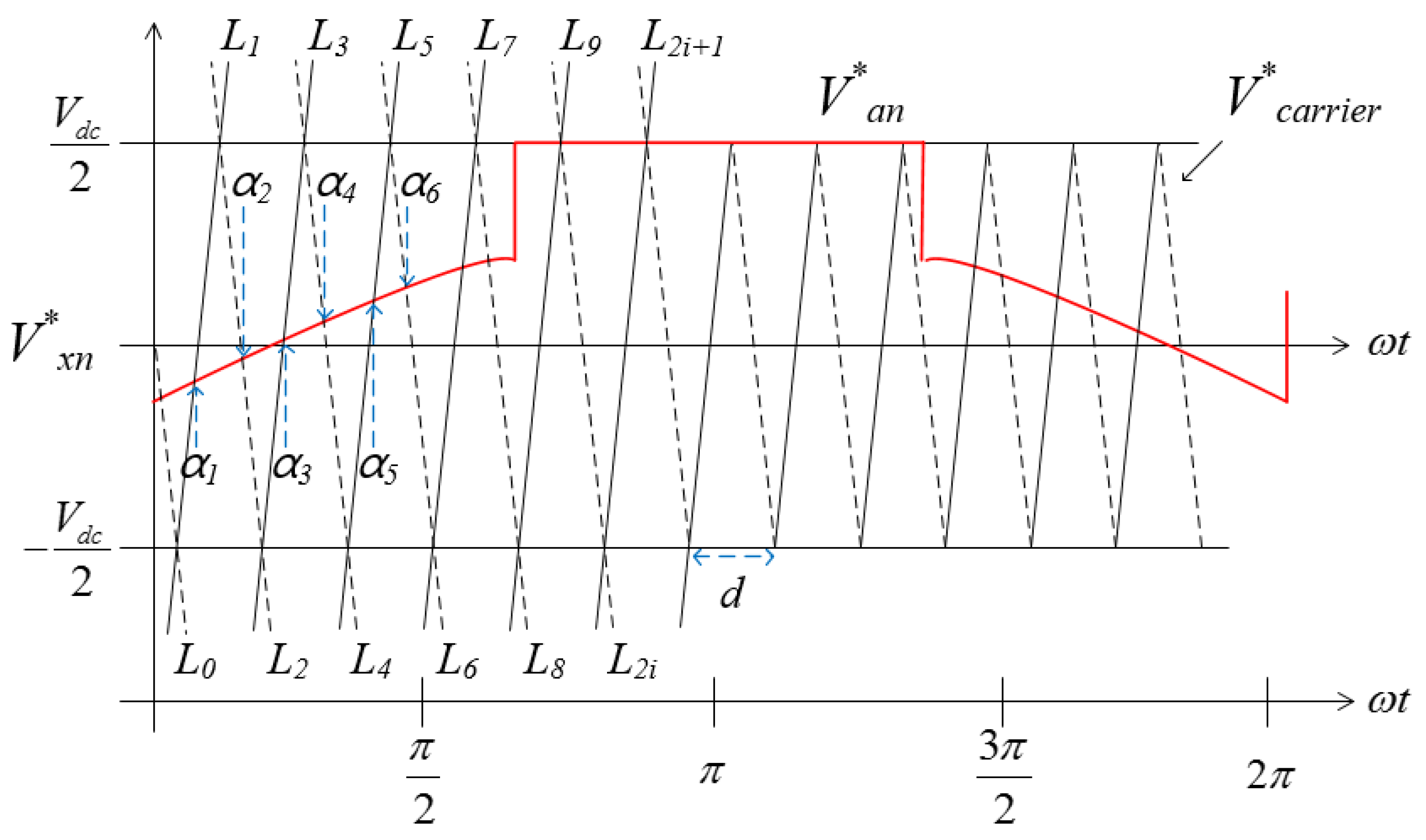
It is necessary to know the switching angle αx to obtain the SSF that has 0.5 or −0.5. αx is determined by the intersection of V*xn and Vcarrier. Therefore, αx can be obtained from the equation representing the intersection of V*xn and Vcarrier. For the convenience of analysis, this paper analyzes the harmonics in the following conditions.
- (1)
If mf (switching frequency/line frequency) is odd, SSF does not include even-order harmonics and has only odd-order harmonics.
- (2)
In this case, SSF becomes the half-wave symmetrical and one cycle of the SSF can be obtained by αx between 0 and 90° (quarter cycle).
Figure 6 shows the method of determining the value of
αx.
Vcarrier can be seen as the sum of the straight lines with the different slopes.
Figure 6 represents the straight lines with different slopes, which are the solid line (
L2i+1) and dotted line (
L2i). All of the intersections of the solid lines and the dotted lines are
Vdc/2 or −
Vdc/2. Therefore, the distance between the straight lines having the same slope is expressed as
From Equation (6), the slopes of the solid and the dotted lines are obtained as
From Equation (7), the equation of a line is determined to
Therefore,
αx can be obtained at the intersection of Equations (5) and (8). From Equations (5) and (8), when considering
V*an, the equation for calculating
αx is follows as
The pattern of
SSF can be constructed through
αx obtained from Equation (9), as shown in
Figure 5.
In this paper, to analyze the harmonic voltages at the output of the inverter,
SSF and the Fourier series are used. By considering the condition (1), the Fourier series can be expressed as
where
n is only odd, and
ω is the radian representation of 60 Hz;
a0,
an,
bn are the Fourier series coefficients.
By substituting the pattern of
SSF into Equation (10), the magnitude of the harmonics is obtained as
where
k is the number of the switching angle.
SSF can be composed of the sum of all harmonics. Therefore, from Equation (11),
SSF is expressed as
If considering the DC-bus voltage as
SSF, the output voltage of the inverter can be obtained. The variation of the output voltage is the half of the DC-bus voltage because the 3-level inverter is considered in this paper. Therefore, from Equation (12), the output voltage of the inverter is expressed as
From Equation (13), the harmonics magnitude of the output voltage is determined as
Equation (14) represents the harmonics magnitude of the
a-phase output voltage. The harmonics magnitudes of the
b-phase and the
c-phase are the same as (14), but have a phase difference of 120°.
To investigate the cause of the resonance, the harmonic analysis of the phase voltage (
Vas,
Vbs,
Vcs =
Vxs) is required.
Vxs is expressed as
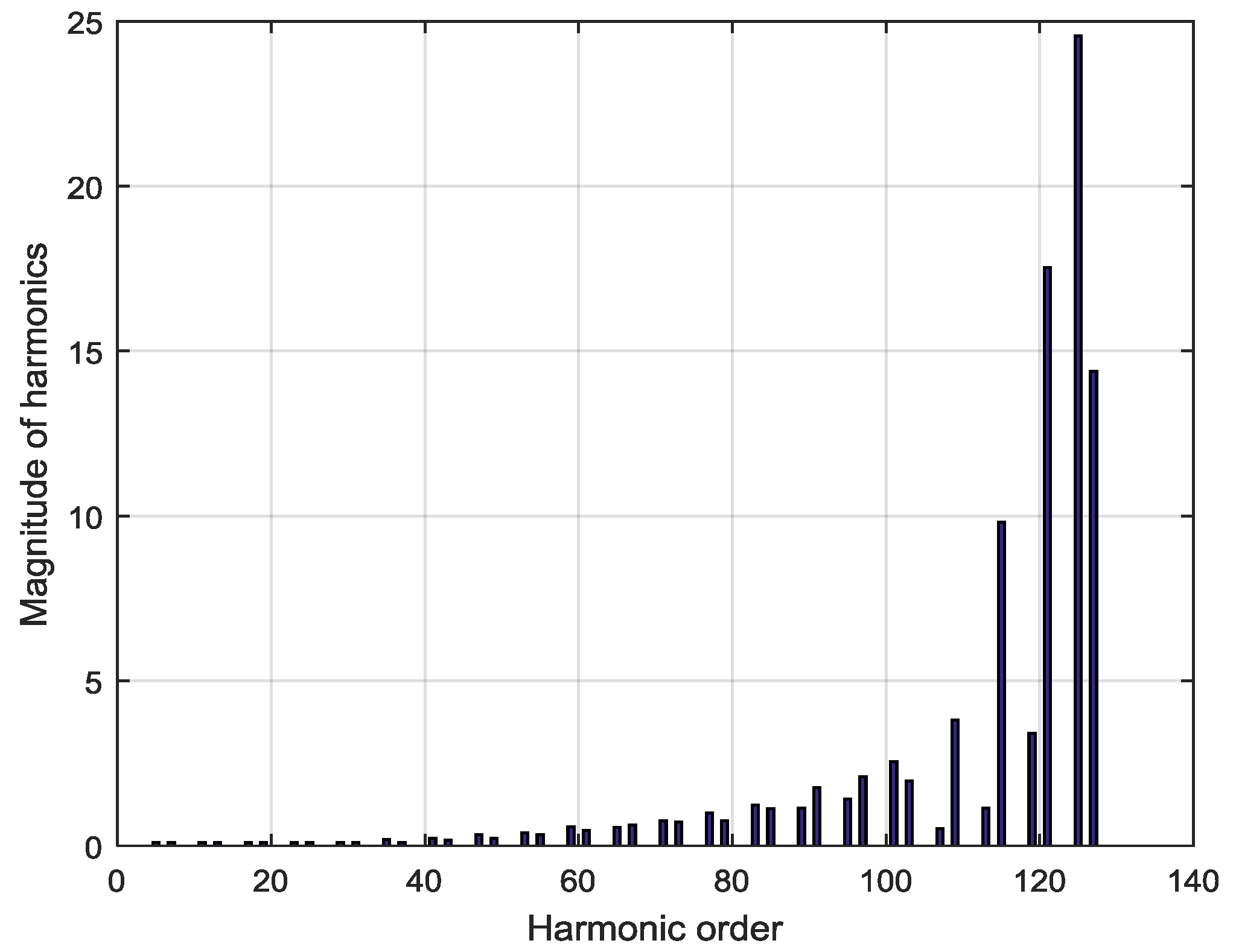
Figure 7 shows the harmonics distribution of
Vxs in simulation condition. To calculate the harmonic components of
Vxs, Matlab simulation is used. From the above-mentioned conditions (1), the switching frequency is approximated to 7740 Hz for the convenience of the analysis, though the actual switching frequency applied in the experiment set is 7800 Hz. N = 1 and 129 harmonics are excluded in
Figure 7 to see the distribution of the lower order harmonics in detail. The harmonics of the switching frequency band have the greatest magnitude. They are distributed in a wide band up to the lower order that is less than the half of the switching frequency. The harmonics in the resonance frequency band by LCL-filter can adversely affect the system because the gain is significant, as shown in
Figure 2. When designing the LCL-filter, to ensure the stability of the system, the resonance frequency is placed in less than the half of the switching frequency to avoid the upper parts of the harmonic spectrum. However, when considering 60° DPWM switching method, the harmonics and the resonance frequency band are overlapped because the lower order harmonics exist in the resonance frequency band. It causes the resonance problem of the grid current. The low order harmonics below the half of the switching frequency are generated at the moment when the modulation signal is clamped to the DC-bus. Consequently, the grid current oscillates every 60° in the conventional DPWM.
5. Proposed Modulation Scheme
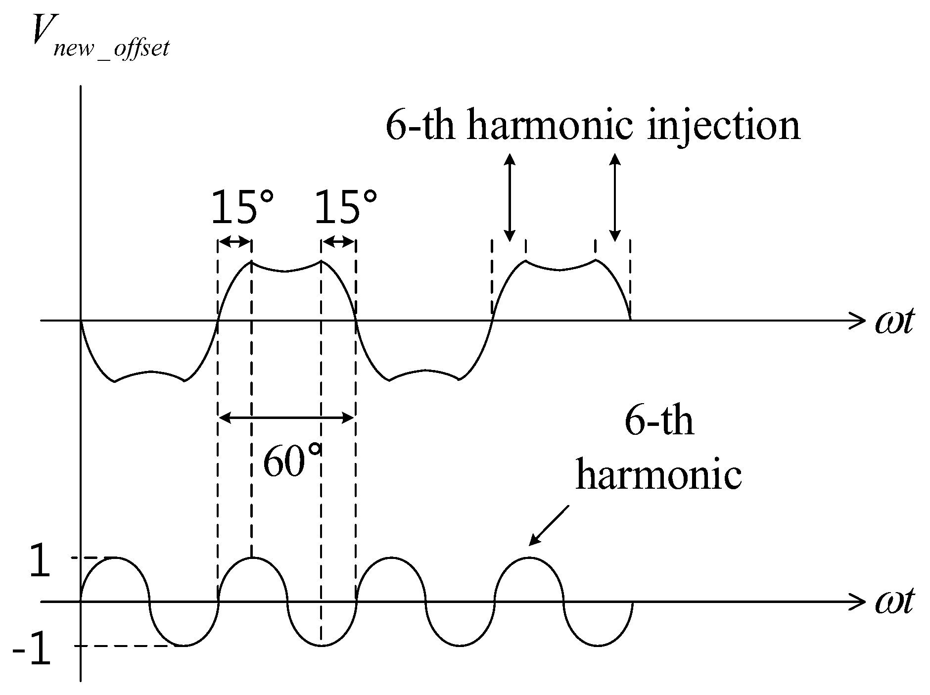
In the conventional DPWM switching method, many harmonic voltages are generated at the output terminal of the inverter due to the discontinuous variation of the modulation signal. This paper introduces new offset voltage
Vnew_offset by using the sixth harmonic injection technique to
Voffset in order to reduce the harmonic voltages, as shown in
Figure 8. The offset voltage of 60° DPWM is changed every 60° and the period of sixth harmonic is same as that of 60°. In the range where the sixth harmonic is injected, sixth harmonic can be easily injected because the direction of change of sixth harmonics and the offset voltage is same. In proposed method, the clamping range of the modulation signals is reduced 30° from 60°. In the case that the maximum value of
V*xs is positive,
Vnew_offset is changed depending on the sixth harmonic during the first and the last 15° range in the clamping range. In the other range,
Vnew_offset can be obtained in the same manner of the 60° DPWM. In the opposite case,
Vnew_offset can be obtained in the same way, as descripted above. To inject proper sixth harmonic, it is necessary to optimize the amplitude of the sixth harmonics. A half period of
Voffset is same as the period of the sixth harmonic because the frequency of the sixth harmonic is twice than that of
Voffset. When considering the unit sixth harmonic that the magnitude is 1, the magnitude of the sixth harmonic is 1 at the point the sixth harmonic injection is completed during the first 15° range. In the same way, at the point the sixth harmonic injection begins during last 15° range, the magnitude of the sixth harmonic is −1. Therefore, to inject the proper sixth harmonic at the second point mentioned above, the magnitude of the sixth harmonic and
Voffset should be same. Therefore, the proposed method uses
Voffset to the magnitude of the sixth harmonic. If
Voffset is used in the magnitude of the sixth harmonic, the optimized sixth harmonic can be injected to
Voffset.
Figure 9 shows the modulation signal of the proposed algorithm.
V*xn is the sum of
V*xs and
Vnew_offset, like Equation (5) for conventional DPWM.
V*xn is expressed as
In the proposed DPWM switching method,
Vnew_offset varies smoothly by injecting the sixth harmonics to
Voffset unlike the conventional DPWM and the modulation signal is softly clamped to the DC-bus, as illustrated in
Figure 9. Therefore, when using the proposed switching method, many harmonics of the output voltage of the inverter can be reduced.
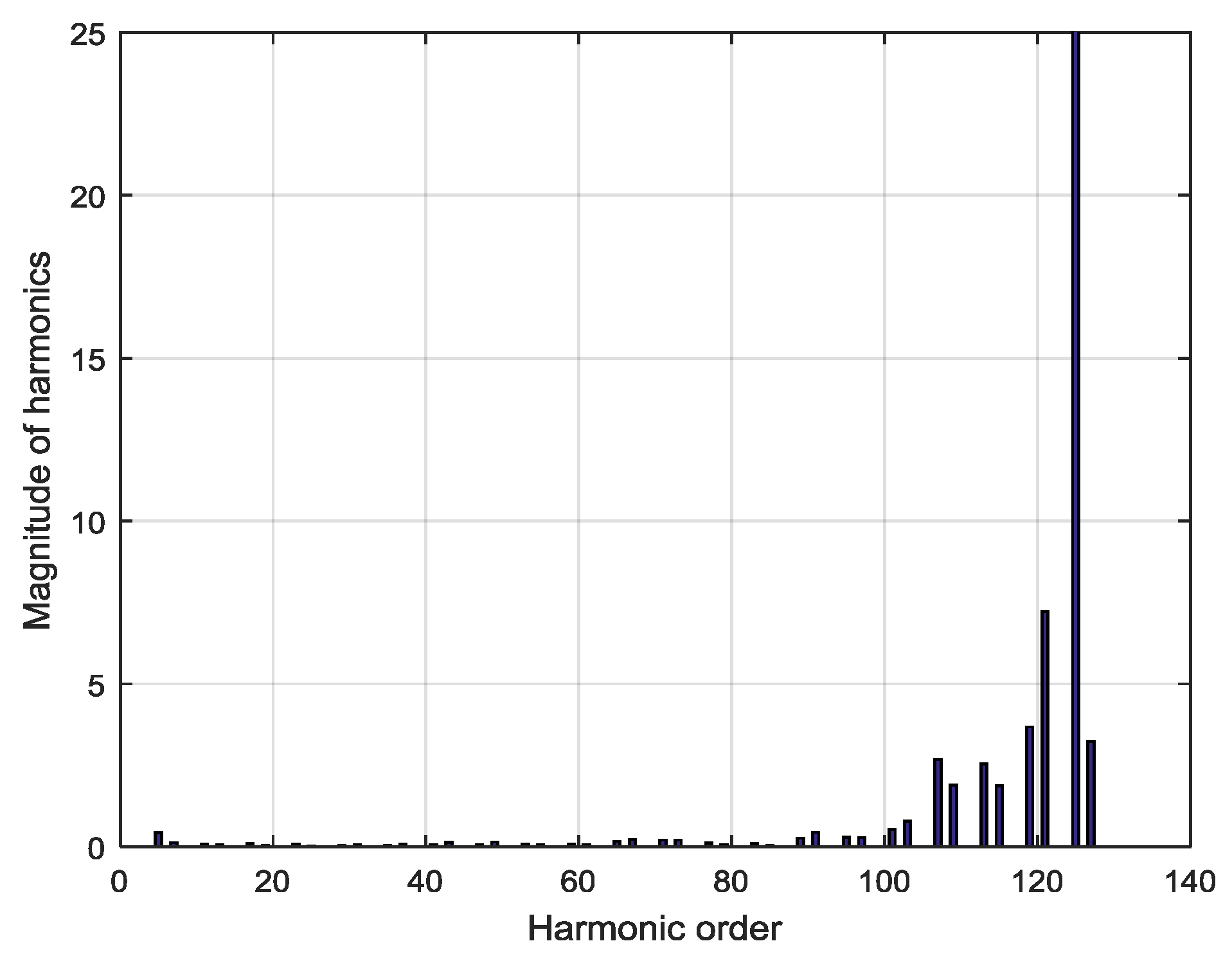
Figure 10 shows the harmonics distribution of
Vsn with the proposed DPWM under the same conditions, as in
Figure 7. N = 1 and 129 harmonics are excluded from
Figure 10, and y-axis scale is the same with that of
Figure 7, which allows to see the lower order harmonics in detail. When the proposed DPWM is implemented to the switching method, the harmonics of the switching frequency band have the greatest magnitude. It is similar to the results, as shown in
Figure 7. However, the distribution of the lower order harmonics is different from that of
Figure 7. In
Figure 10, the harmonics below N = 100 are reduced and are not distributed in a wide frequency range when compared with that of
Figure 7. Therefore, the lower order harmonics that are less than the half of the switching frequency are also reduced. If the harmonic voltages overlap the resonance frequency band caused by the LCL-filter, the problem of the resonance current does not occur because the harmonic voltages in the resonance frequency band are sufficiently reduced. Consequently, the grid current does not oscillate every 60° when the modulation signal is clamped to the DC-bus.
The proposed method uses sixth harmonic injection technique to reduce the resonance current. When using this method, the quality of the grid current is improved because the resonance components of the grid current can be sufficiently reduced. However, the proposed DPWM has a disadvantage regarding the efficacy because the clamping range is too narrow to inject sixth harmonics to Voffset.
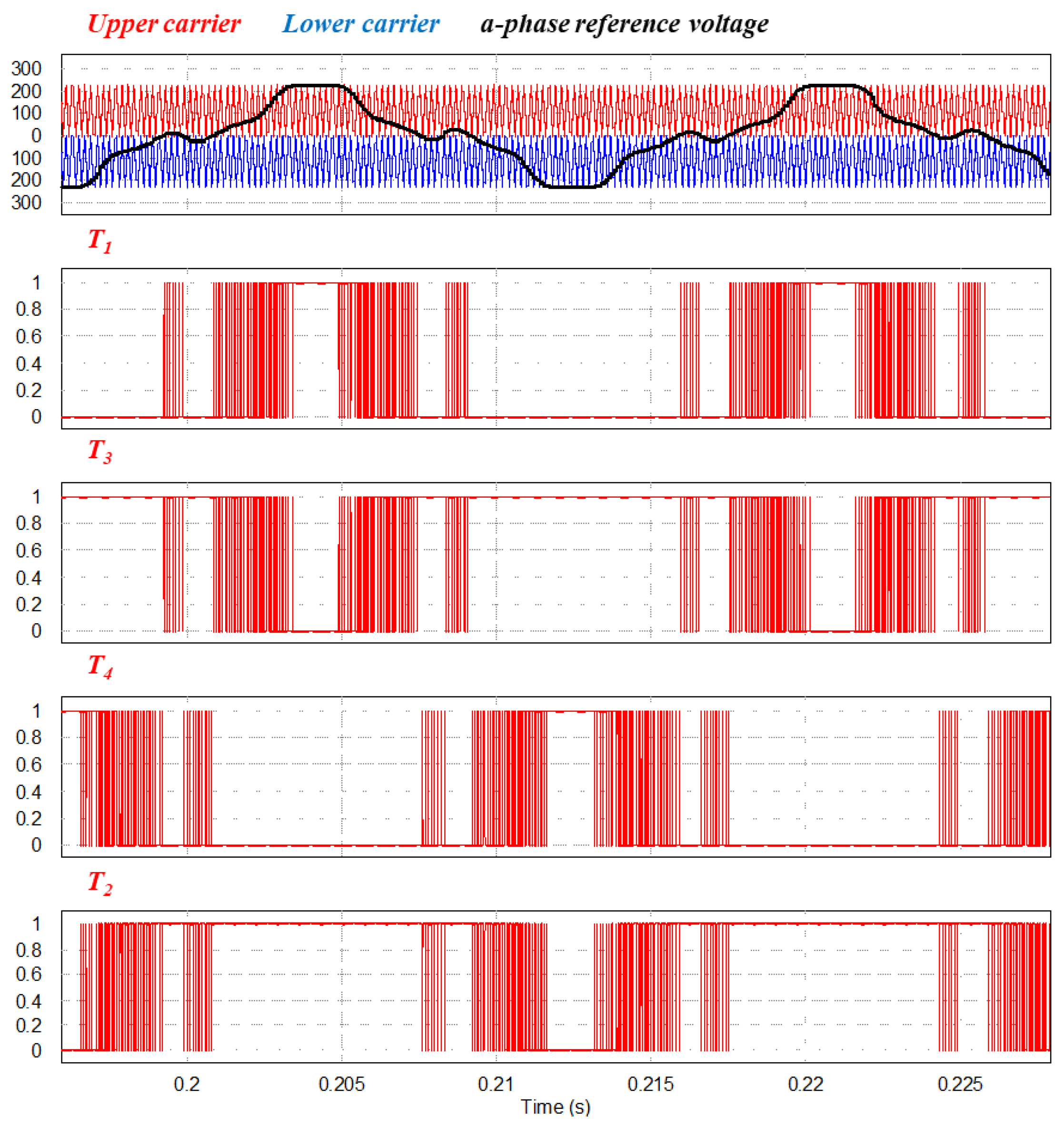
Figure 11 shows switching states of three-level inverter with the proposed DPWM (
T1,
T2,
T3, and
T4 are shown in
Figure 1). If the a-phase reference voltage is positive, it is compared with the upper carrier signal and
T1,
T3 are triggered.
T1 and
T3 operate complementarily.
T2 and
T4 maintains ON and OFF state. In the opposite case, the reference voltage is compared with lower carrier signal and
T2,
T4 are triggered.
T2 and
T4 also operate complementarily.
T3 and
T1 maintains ON and OFF state. The switches of b- and c-phase are triggered in the same way, according to the reference voltage.
6. Simulation Results
To confirm the validity of the proposed algorithm, a simulation was performed using a Powersim (PSIM) simulation (Powersim Inc., Rockville, MD, USA). The simulation circuit is the same as
Figure 1. The simulation parameters are given in
Table 1.
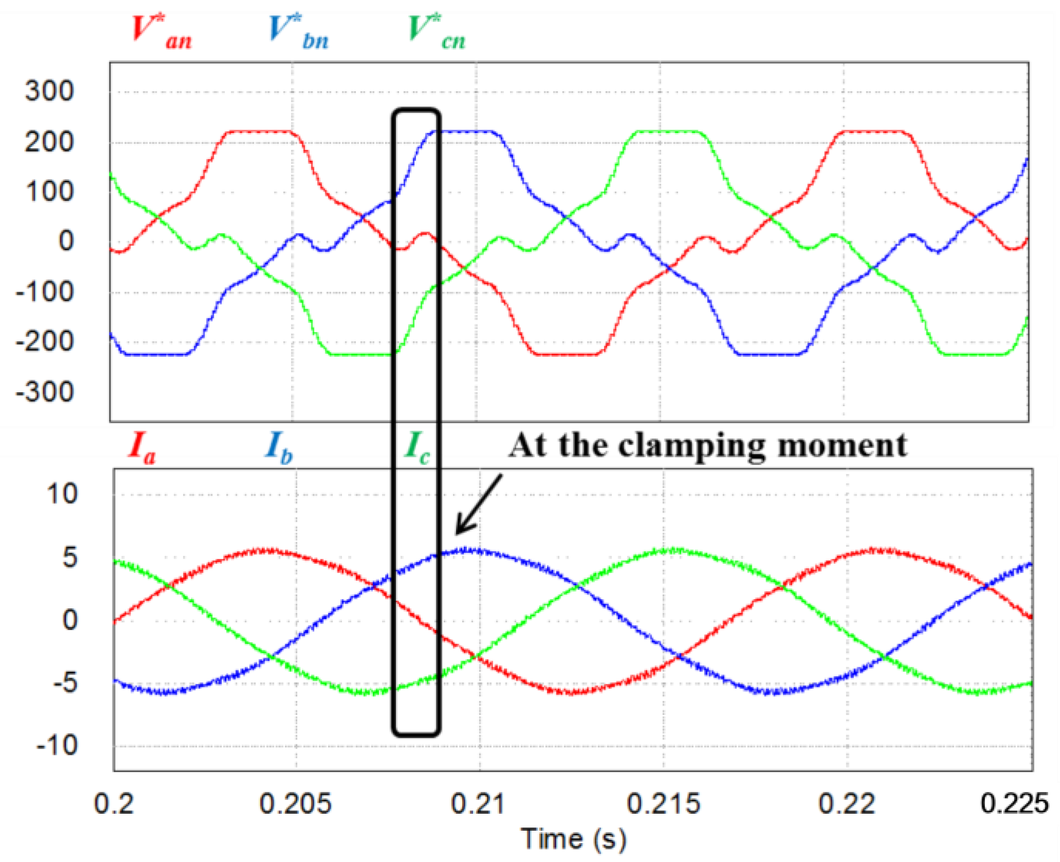
Figure 12 shows
V*an,
Voffset, and the grid current of the conventional DPWM.
V*xn is clamped to the DC-bus by
Voffset.
Vxs has a number of harmonic voltages and these harmonics are generated at the moment when
V*xn is clamped to the DC-bus. In the conventional DPWM switching method, the harmonic voltages are distributed in the wide frequency range. The harmonics also exist in the resonance frequency band. From Equation (1),
fresonance is obtained as 3495 Hz by the LCL-filter and the resonance frequency band is formed around
fresonance. In the simulation condition,
fresonance overlaps the harmonic voltages of
Vxs. Therefore, the grid current oscillates at the moment that
V*xn is clamped to the DC-bus every 60°, as shown in
Figure 12.
Figure 13 shows the performance of the proposed algorithm. The system operates under the same condition, as in
Figure 12. The proposed method injects the sixth harmonic to
Voffset to reduce many harmonics of
Vxs.
V*xn is continuously clamped to the DC-bus as shown in
Figure 13. It is possible to reduce many harmonics of
Vxs because the discontinuous variation of
Voffset disappears.
fresonace is still 3495 Hz by the LCL-filter. However, the harmonic voltages are sufficiently reduced. In particular, the harmonics of the resonance frequency band also are reduced. Therefore, the grid current does not oscillate at the moment that
V*xn is clamped to the DC-bus.
7. Experimental Results
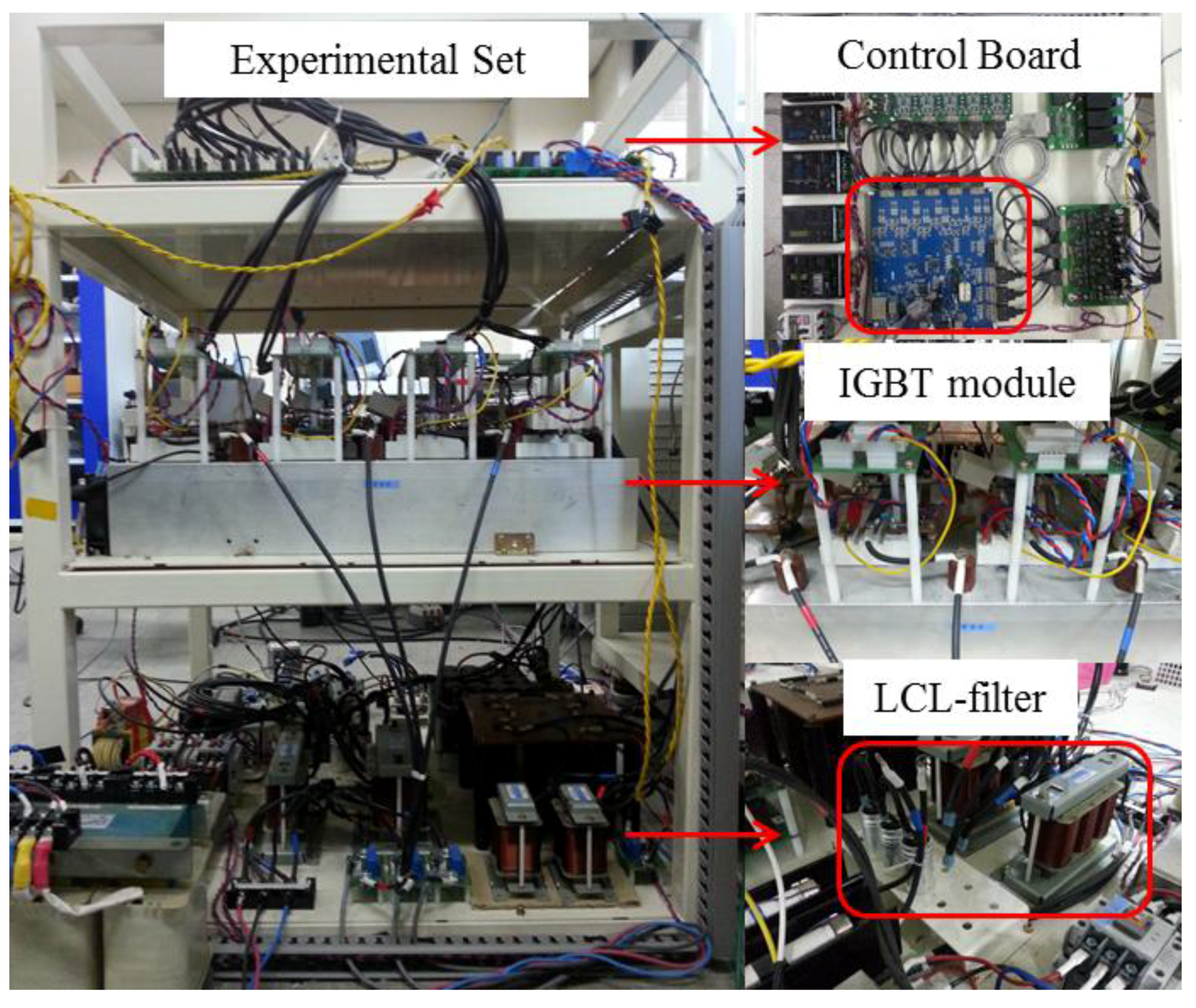
The Experiments were performed to verify the proposed method.
Figure 14 shows the hardware setup. This set consists of a control board, a sensor board, gate drivers, and LUH50G1204 IGBT modules from LSIS (LS Industrial Systems Co., Ltd., Anyang-si, Korea). The experimental setup parameters are the same as the simulation parameters, as shown in
Table 1.
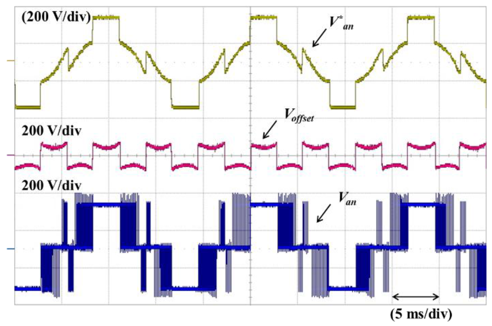
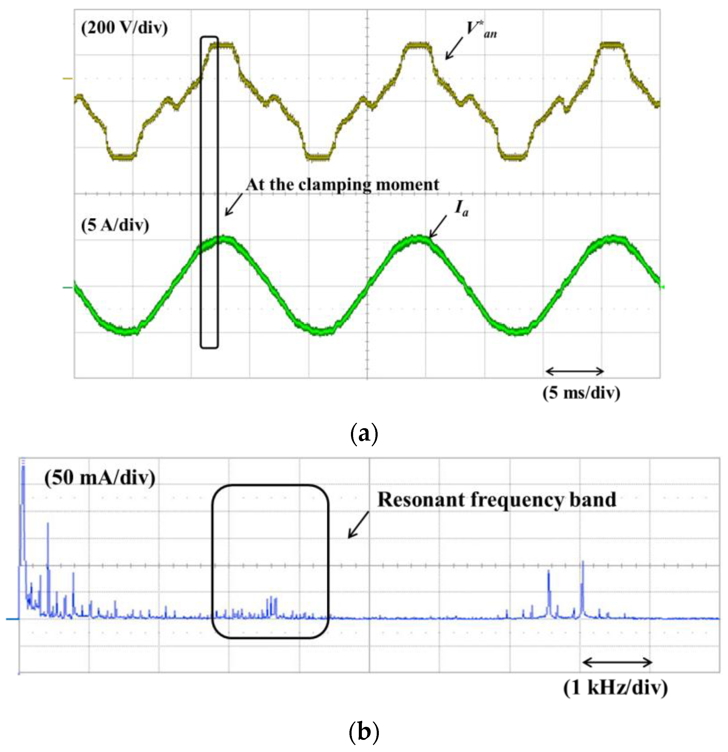
Figure 15 shows the reference of the a-phase pole voltage
V*an,
Voffset, and the a-phase pole voltage
Van in the conventional DPWM.
Voffset discontinuously changes every 60°.
V*an is clamped to the DC-bus as the variation of
Voffset. In accordance with
V*an,
Van is also clamped to the DC-bus and
Van maintains the DC-link voltage in the clamping range because the switching device is not switched.
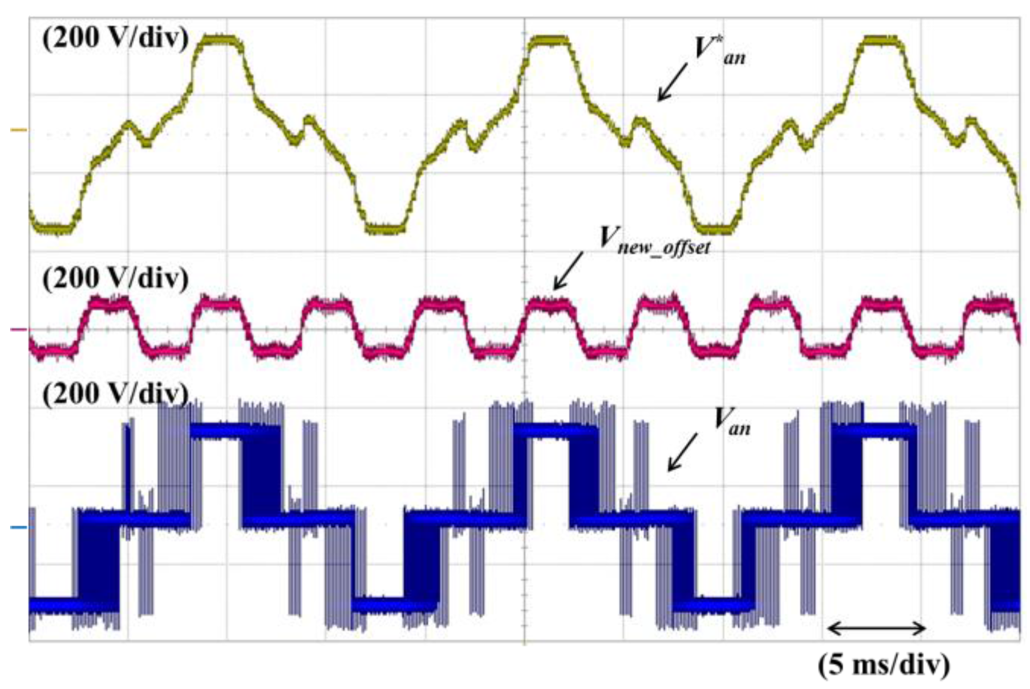
Figure 16 shows the
V*an,
Vnew_offset, and
Van of the proposed DPWM.
Vnew_offset smoothly changes every 60° when compared with
Voffset, as shown in
Figure 14, because the proposed method injects the sixth harmonic to
Voffset. This method can soften the variation of
V*an when
V*an is clamped to the DC-bus. In the proposed algorithm, the clamping range is too narrow when compared with that of the conventional DPWM due to the range where the 6-th harmonic is injected. For the reasons described above, the range in which
Van maintains the DC-link voltage is narrow compared with
Figure 15.
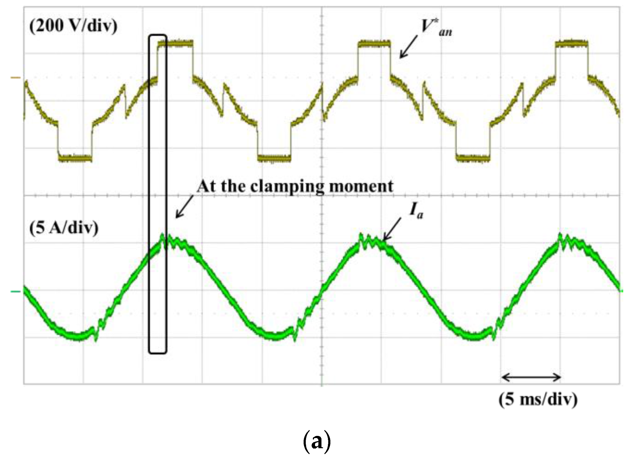
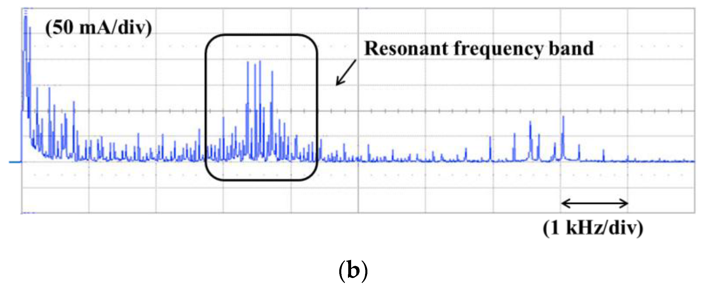
Figure 17 shows the
V*an and the a-phase grid current
Ia in the conventional DPWM.
Vas has many harmonic components, which are generated at the clamping moment where
V*an is discontinuously changed. When these harmonic frequencies overlap
fresonance, the resonance problem of the grid current occurs.
Figure 17a shows the resonance problem of the grid current. As mentioned above,
Ia oscillates at the clamping moments, as shown in
Figure 17a. When using the conventional DPWM, the efficiency of the system is improved because the switching devices are not switched in the clamping range. However, the resonance of the grid current causes the problem that adversely affects the quality of the grid current.
Figure 17b shows the harmonics of
Ia in the frequency domain.
Ia has many harmonics, particularly in the resonance frequency band. The magnitude of the resonance components of
Ia is approximately 0.2 A, as shown in
Figure 17b.
Figure 18 shows the performance of the proposed DPWM. Unlike
V*an shown in
Figure 17a,
V*an continuously changes, as shown in
Figure 18a. Many harmonics of
Vas are reduced because the sixth harmonic injection technique smoothly modifies
V*an. Therefore,
Ia does not oscillate at the clamping moment, as shown in
Figure 18a.
Figure 18b shows
Ia in the frequency domain. When comparing with the result of
Figure 17b, many harmonics of
Ia in the resonance frequency band are sufficiently reduced. The magnitude of the resonance component of
Ia is approximately 0.04 A, as shown in
Figure 18b.
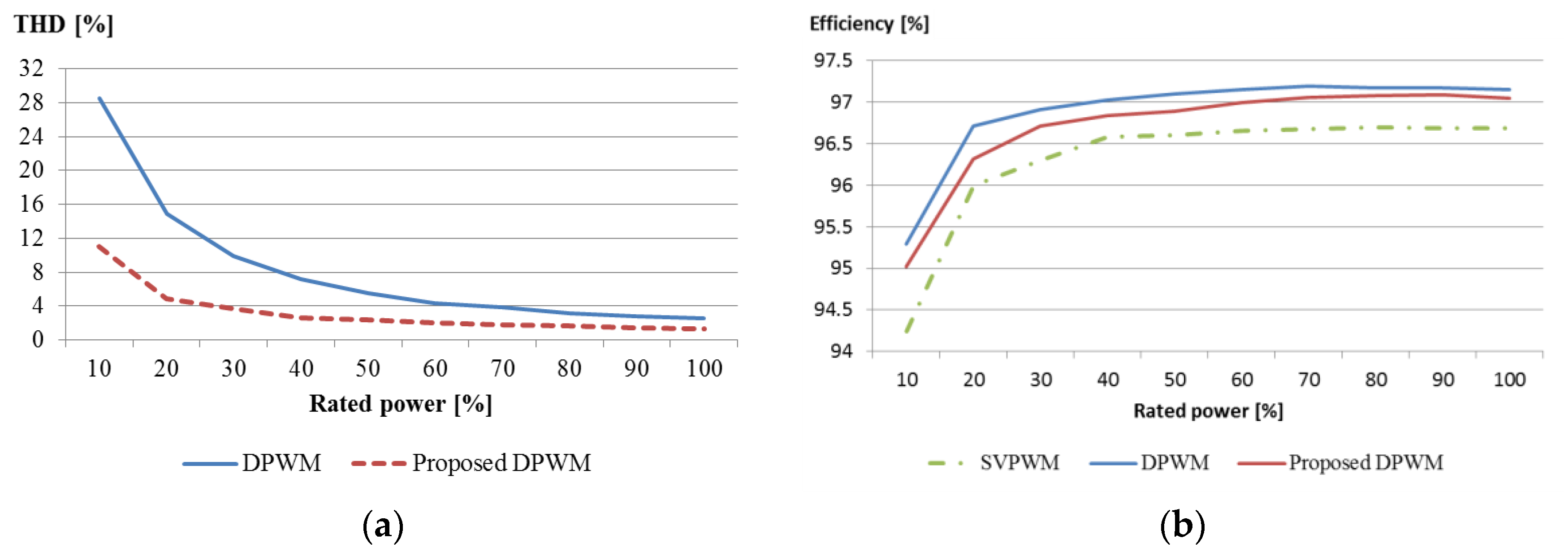
Figure 19 compares the efficiency and the THD of the grid current, according to the switching methods. The THD and the efficiency were measured using the WT3000 power analyzer (YOKOGAWA, Tokyo, Japan). In
Figure 19a, the THD of the conventional DPWM and the proposed DPWM are compared according to the loads. In the conventional DPWM, the grid current has the resonant components, which adversely affect the THD. However, the proposed DPWM improves the THD when compared with that of the conventional DPWM because the proposed DPWM can reduce the resonance current.
Figure 19a shows the result that the THD of the proposed DPWM is lower than that of the conventional DPWM for the entire load range.
Figure 19b shows the efficiency of three modulation signals: SPWM, the conventional DPWM, and the proposed DPWM. The conventional DPWM and the proposed DPWM have the advantage of the lower switching loss because both methods have a clamping range where the switching devices are not operated. Therefore, the efficiency of both modulation methods is 1% higher than that of the SPWM. When comparing the conventional DPWM and the proposed DPWM, the clamping range of the proposed DPWM is narrower than that of the conventional DPWM because the proposed DPWM has the region where the sixth harmonic is injected. For this reason, the efficiency of the proposed DPWM is slightly lower than that of the conventional DPWM because the switching loss of the proposed DPWM is higher than that of the conventional DPWM.


