A Study of Two Multi-Element Resonant DC-DC Topologies with Loss Distribution Analyses


Abstract
:1. Introduction
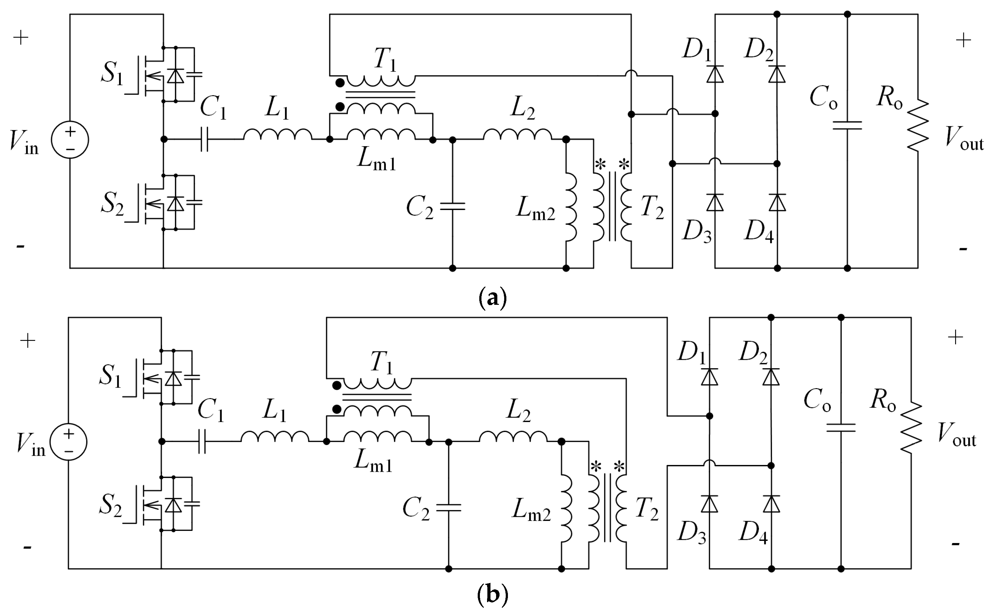
2. Operating Principle of the Proposed Converter
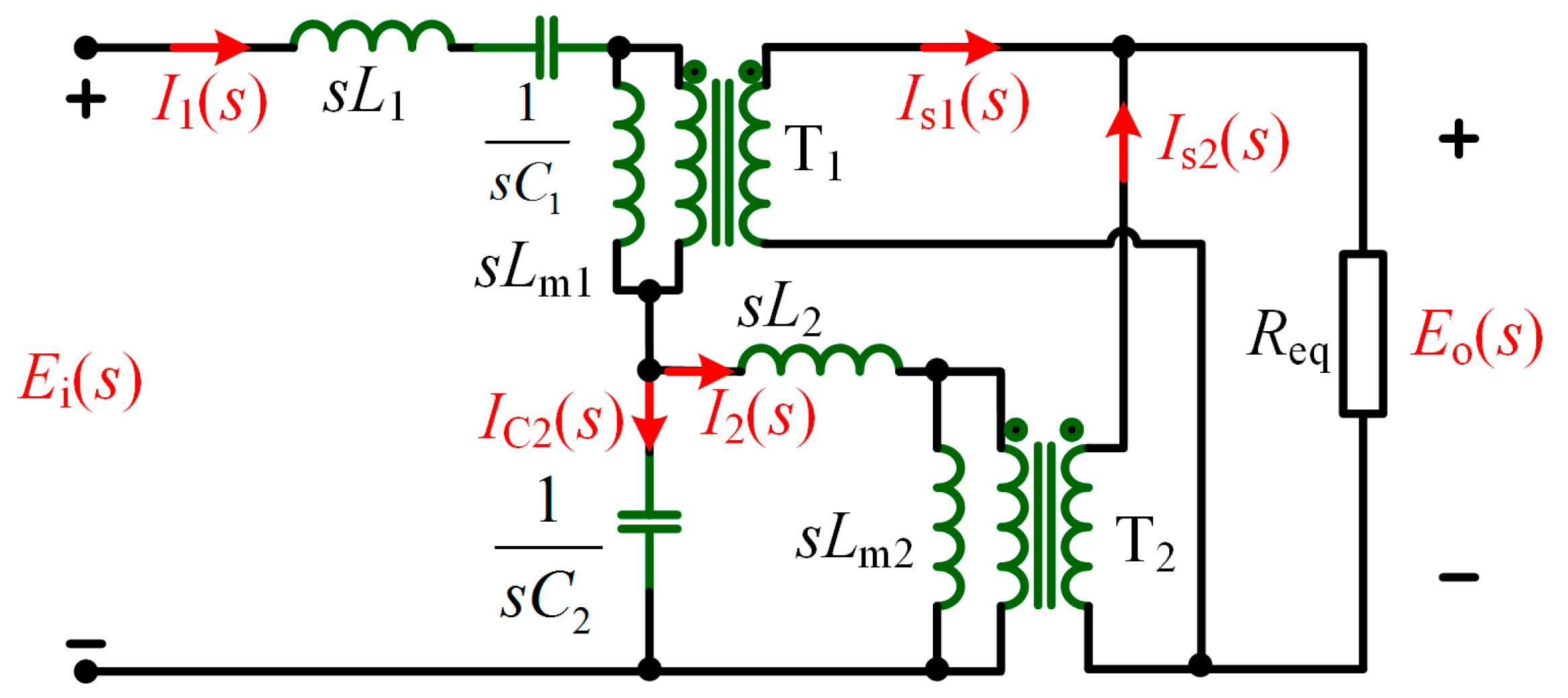
3. Steady-State Analysis
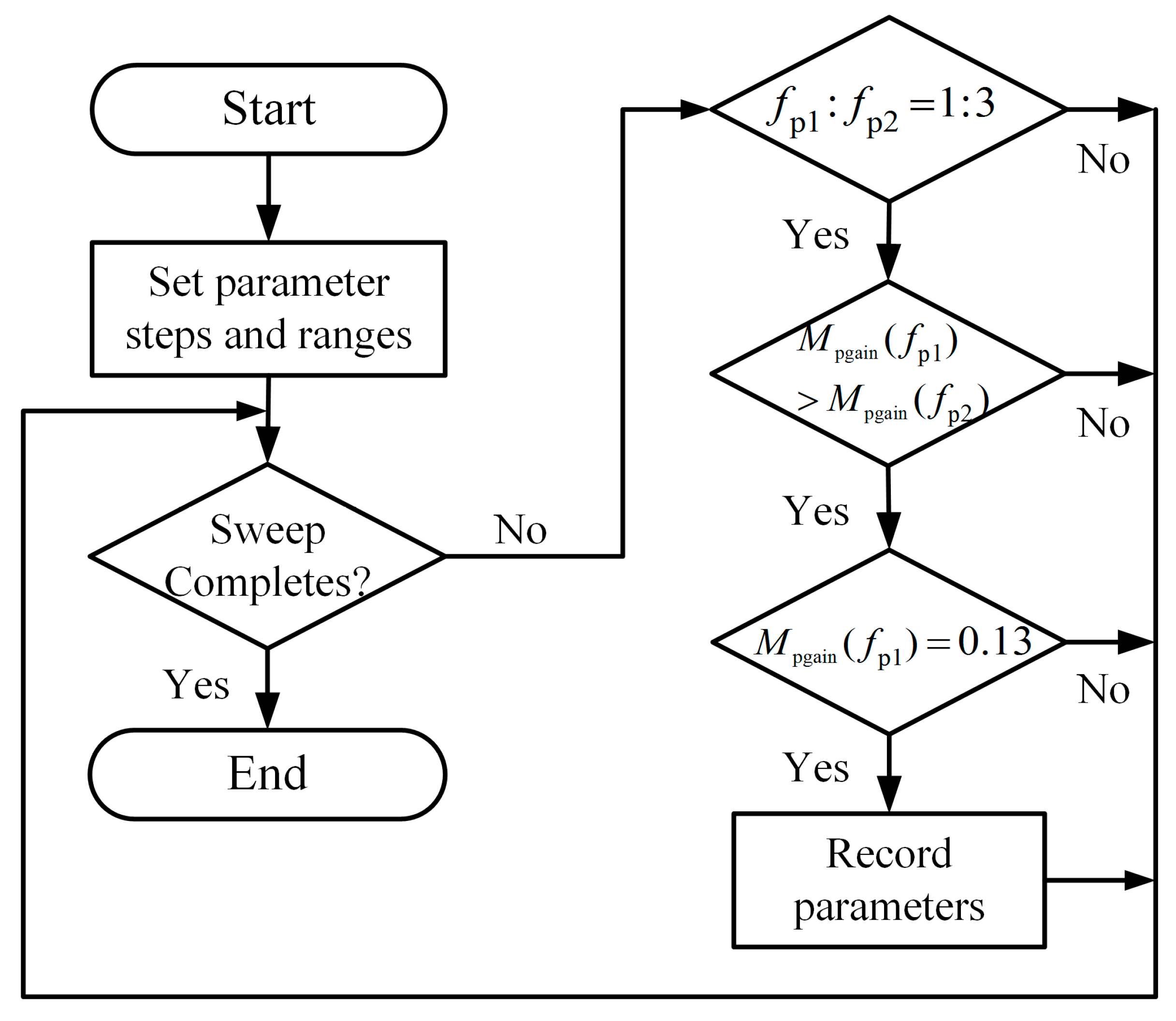
4. Parameters Optimization Design
4.1. Selection Constraints of the Parallel Topology
4.2. Selection Constraints of the Serial Topology
- (a)
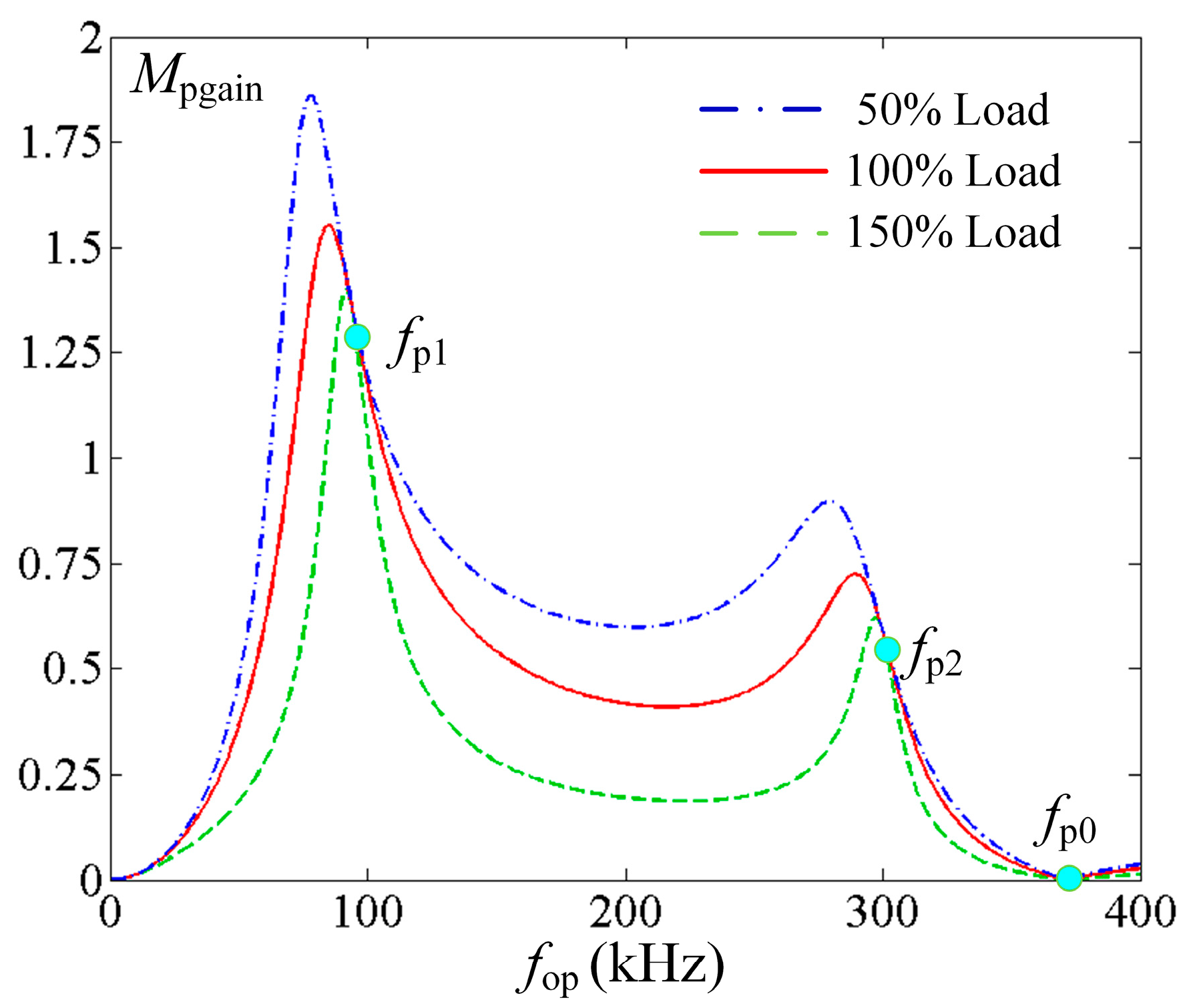
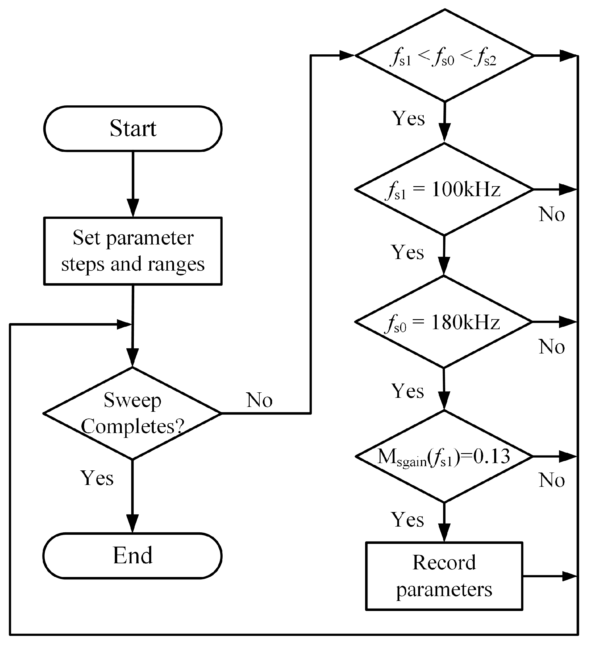
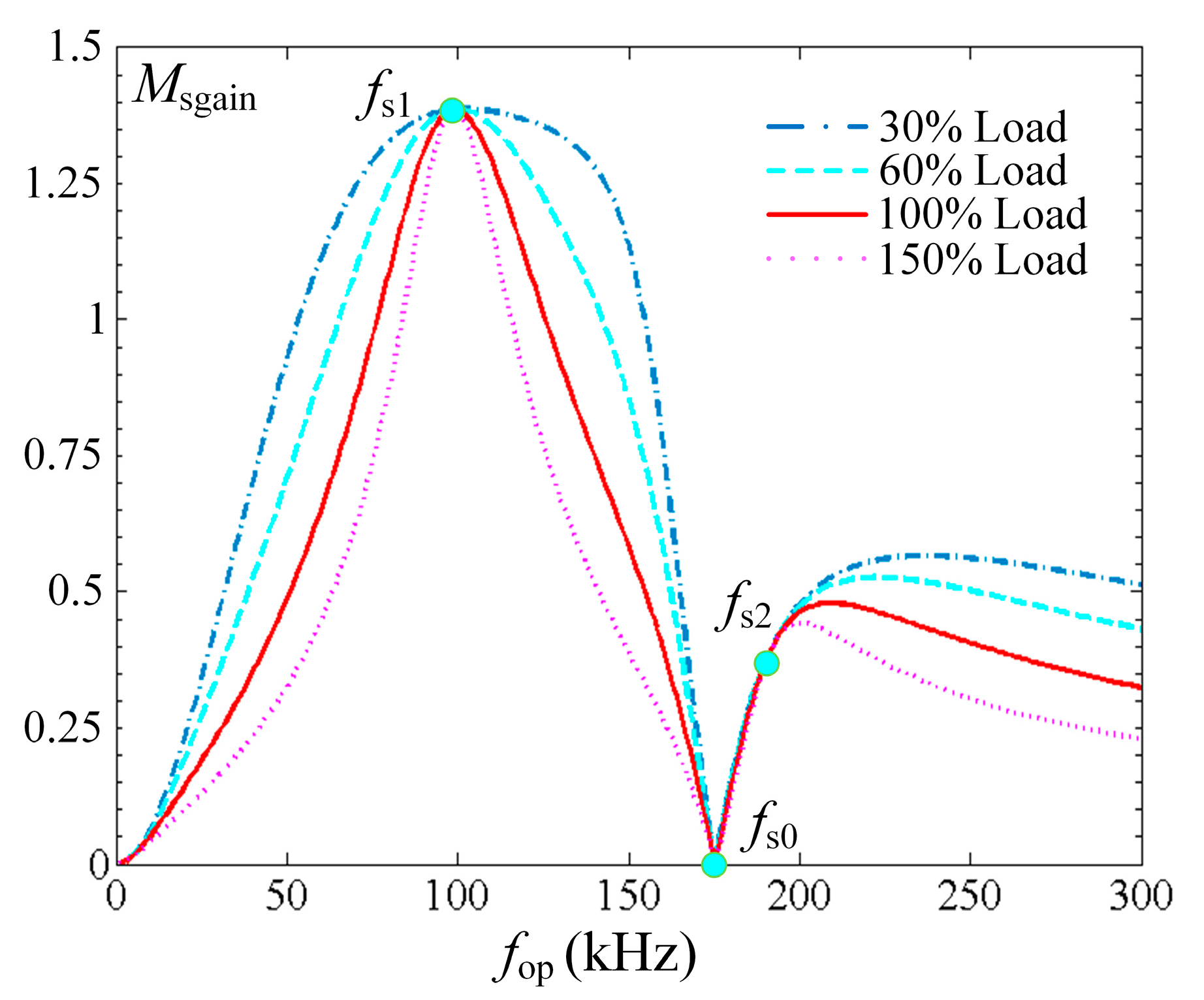
- fs1 < fs0 < fs2. According to Equations (10) and (11), the three resonant points should be set as this inequation, so that the gain curve is consistent with Figure 4. Since the ZVS region is from fs1 to fs0, the serial converter obtains widely adjustable gain range within this scope.
- (b)
- fs1 = 100 kHz. The rated operating frequency should be set closely enough to the resonant point fs1, and thereby fs1 is set at 100 kHz here.
- (c)
- fs0 = 180 kHz. Msgain(fs0) stays at zero theoretically and contributes to wide voltage gain range starting from zero. If fs0 is far away from fs1, the converter must increase the operating frequency significantly to achieve wide gain range, which will inevitably introduce high frequency losses. Meanwhile, when fs0 is too close to fs1, then the circulating energy will be enhanced as the following outcomes, since the input impedance angle is elevated dramatically. In this case, fs0 is set at 180 kHz as the compromise result.
- (d)
- Msgain(fs1) = 0.13. Same with the parallel dual-CLT converter, the rating input and output voltages are also set at 400 V and 52 V.
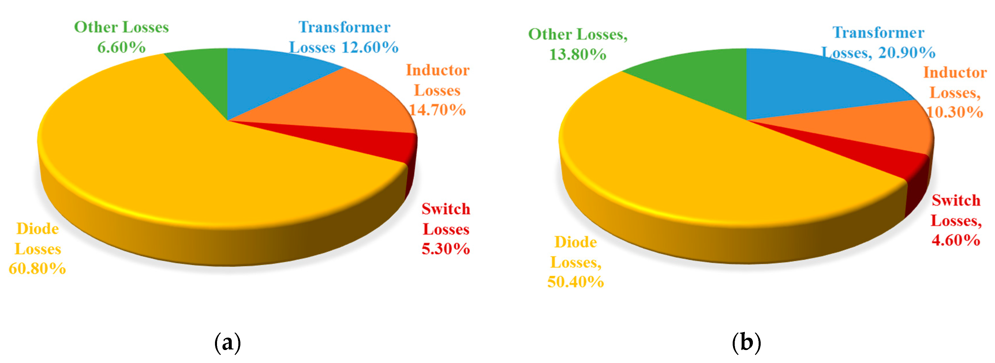
5. Loss Distribution Analyses
5.1. Transformer Losses
5.2. Inductor Losses
5.3. Power Switch Losses
5.4. Diode Losses
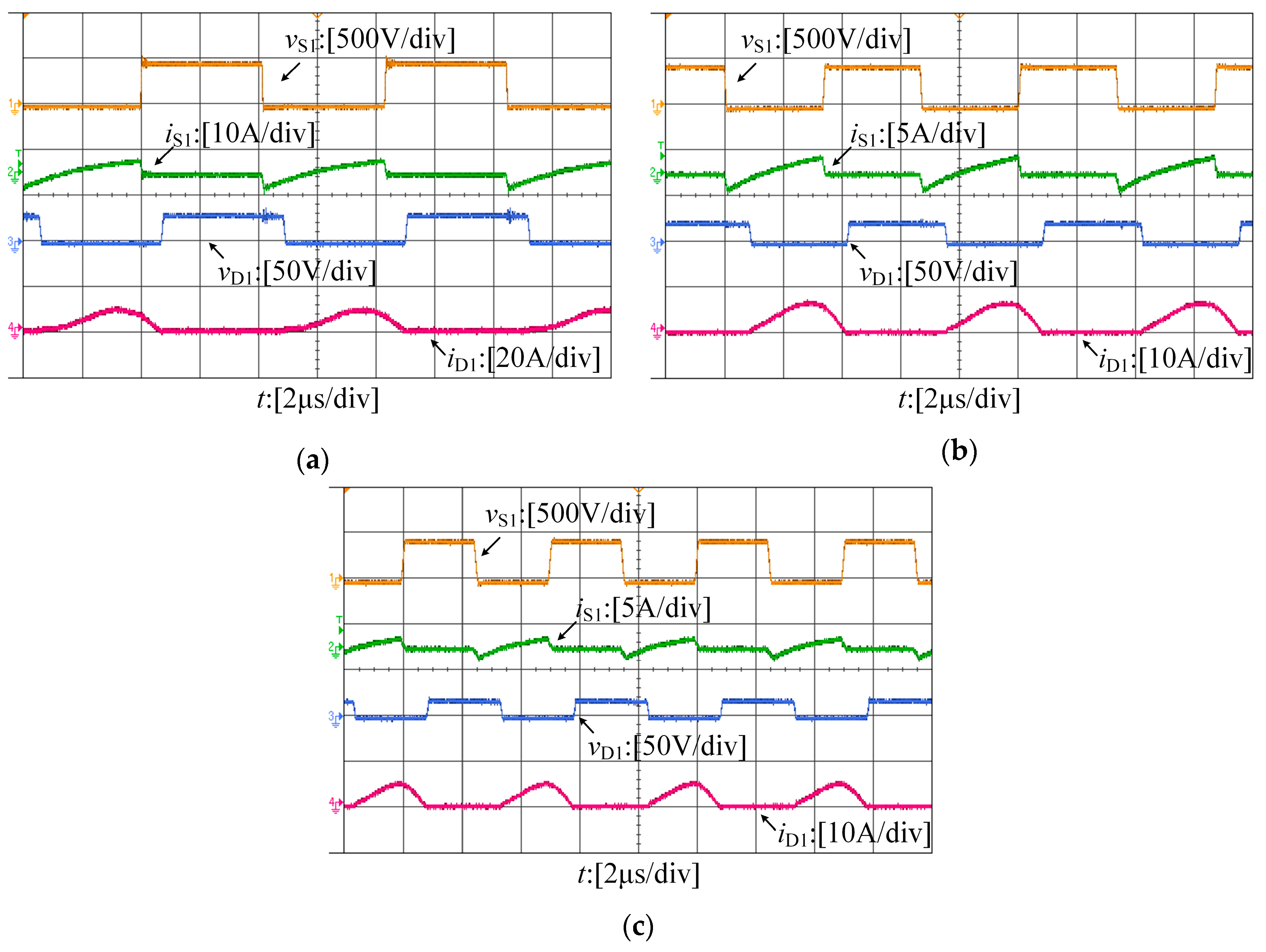
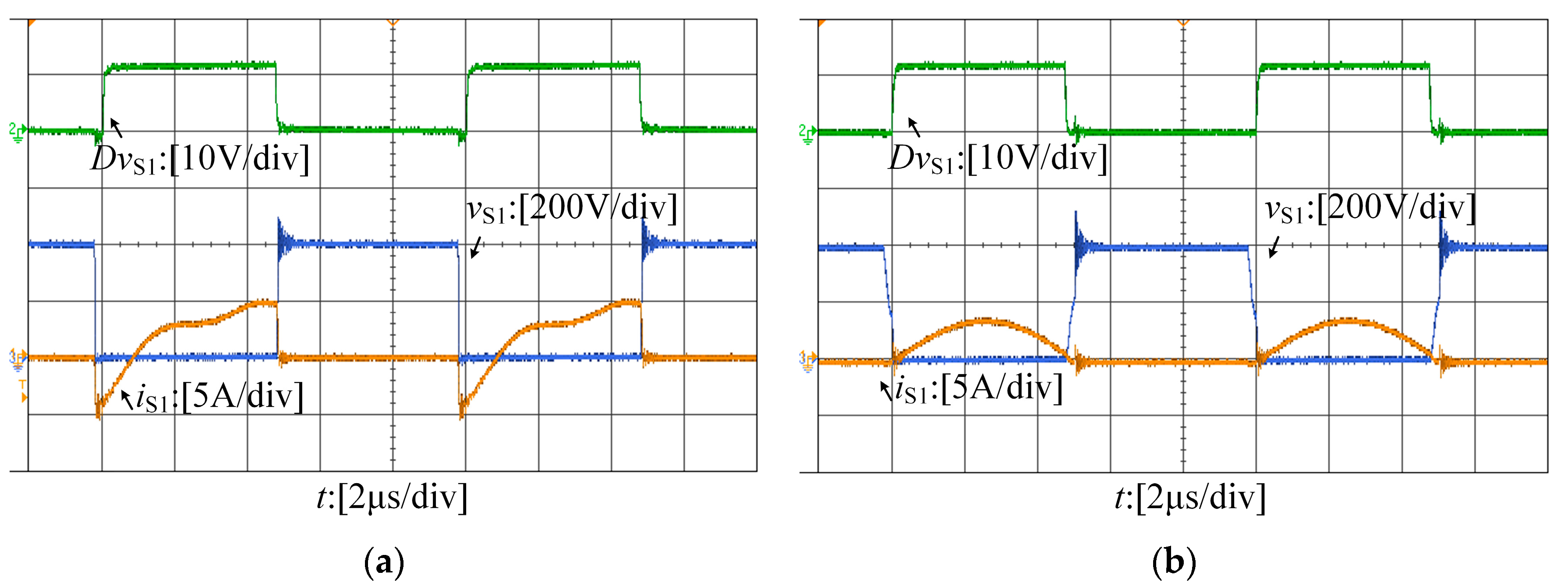
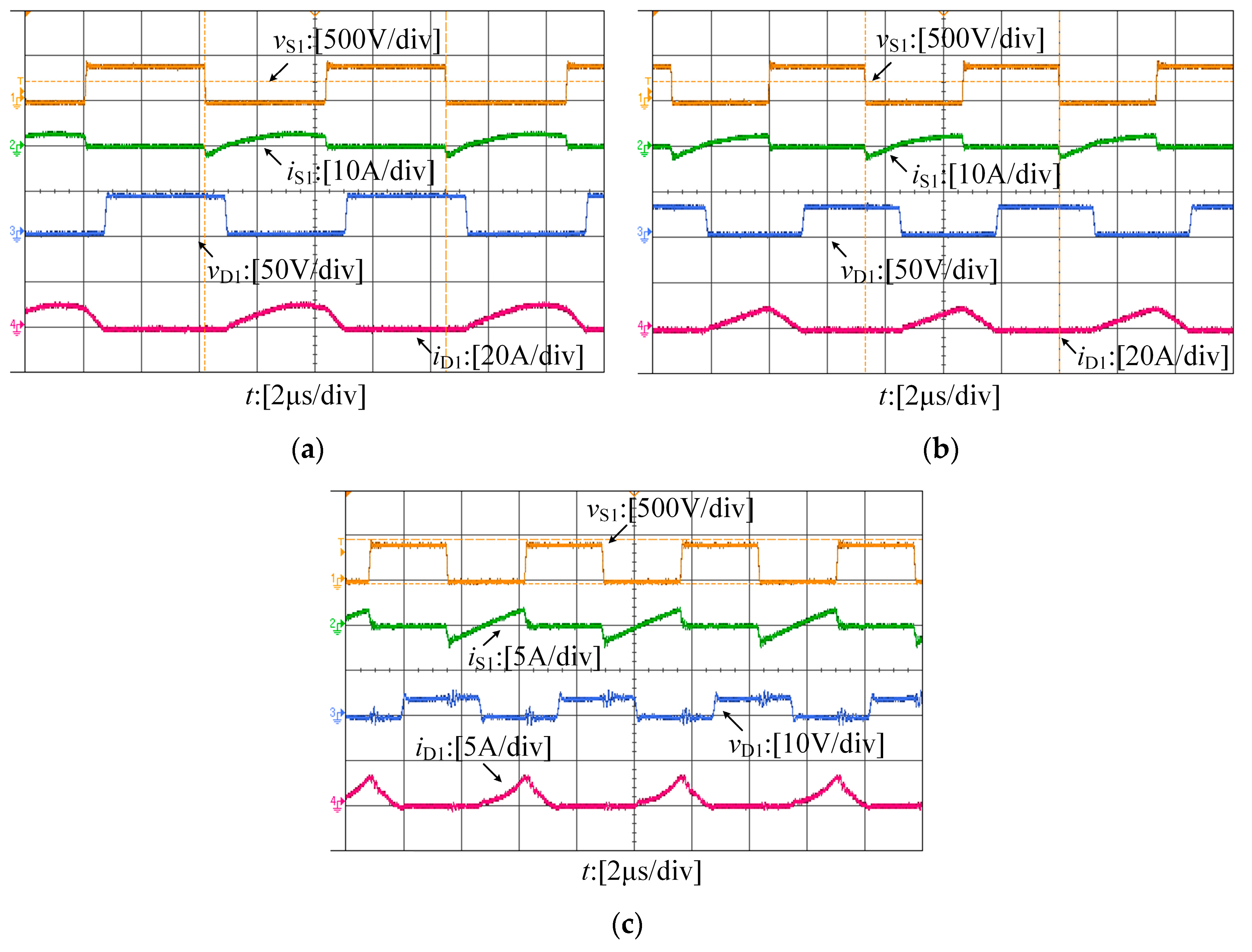
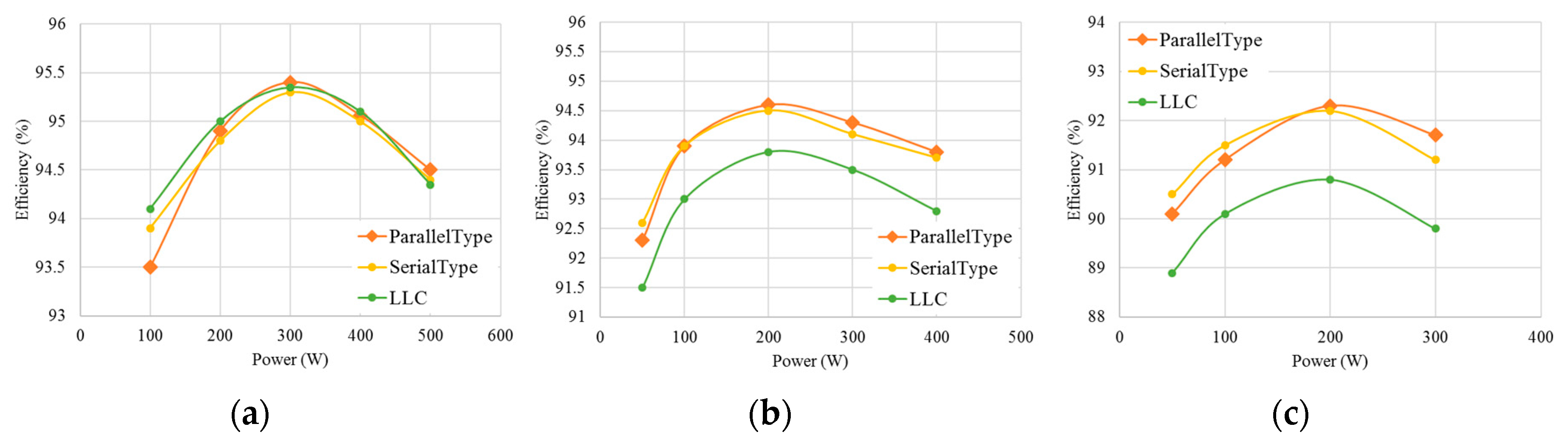
6. Experiments
7. Conclusions
Acknowledgments
Author Contributions
Conflicts of Interest
References
- Li, H.Y.; Li, X.; Lu, M.; Hu, S. A linearized large signal model of an LCL-type resonant converter. Energies 2015, 8, 1848–1864. [Google Scholar] [CrossRef]
- Wang, C.S.; Li, W.; Wang, Y.F.; Chen, B. A high-efficiency isolated LCLC multi-resonant three-port bidirectional DC-DC converter. Energies 2017, 10, 934. [Google Scholar] [CrossRef]
- Deng, J.; Li, S.; Hu, S.; Mi, C.C.; Ma, R. Design methodology of LLC resonant converters for electric vehicle battery chargers. IEEE Trans. Veh. Technol. 2014, 63, 1581–1592. [Google Scholar] [CrossRef]
- Hu, S.; Deng, J.; Mi, C.; Zhang, M. Optimal design of line level control resonant converters in plug-in hybrid electric vehicle battery chargers. IET Electr. Syst. Transp. 2013, 4, 21–28. [Google Scholar] [CrossRef]
- Tan, X.; Ruan, X. Equivalence relations of resonant tanks: A new perspective for selection and design of resonant converters. IEEE Trans. Ind. Electr. 2016, 63, 2111–2123. [Google Scholar] [CrossRef]
- Beiranvand, R.; Rashidian, B.; Zolghadri, M.R.; Alavi, S.M.H. Optimizing the normalized dead-time and maximum switching frequency of a wide-adjustable-range LLC resonant converter. IEEE Trans. Power Electr. 2011, 26, 462–472. [Google Scholar] [CrossRef]
- Beiranvand, R.; Rashidian, B.; Zolghadri, M.R.; Alavi, S.M.H. A design procedure for optimizing the LLC resonant converter as a wide output range voltage source. IEEE Trans. Power Electr. 2012, 27, 3749–3763. [Google Scholar] [CrossRef]
- Fang, X.; Hu, H.; Chen, F.; Somani, U.; Auadisian, E.; Shen, J.; Batarseh, I. Efficiency-oriented optimal design of the LLC resonant converter based on peak gain placement. IEEE Trans. Power Electr. 2012, 28, 2285–2296. [Google Scholar] [CrossRef]
- Hu, S.; Li, X.; Lu, M.; Luan, B.-Y. Operation modes of a secondary-side phase-shifted resonant converter. Energies 2015, 8, 6098–6113. [Google Scholar] [CrossRef]
- Jang, J.; Joung, M.; Choi, S.; Choi, Y.; Choi, B. Current mode control for LLC series resonant DC-to-DC converters. Energies 2014, 14, 21–27. [Google Scholar]
- Han, J.H.; Lim, Y.C.; Sciubba, E. Design of an LLC resonant converter for driving multiple LED lights using current balancing of capacitor and transformer. Energies 2015, 8, 2125–2144. [Google Scholar] [CrossRef]
- Jiang, T.; Zhang, J.; Wu, X.; Sheng, K.; Wang, Y. A bidirectional LLC resonant converter with automatic forward and backward mode transition. IEEE Trans. Power Electr. 2014, 30, 757–770. [Google Scholar] [CrossRef]
- Jiang, T.; Chen, X.; Zhang, J.; Wang, Y. Bidirectional LLC resonant converter for energy storage applications. In Proceedings of the IEEE Applied Power Electronics Conference and Exposition, Long Beach, CA, USA, 17–21 March 2013; pp. 1145–1151. [Google Scholar]
- Mu, M.; Lee, F.C. Design and optimization of a 380–12 V high-frequency, high-current LLC converter with GaN devices and planar matrix transformers. IEEE J. Emerg. Sel. Top. Power Electr. 2016, 4, 854–862. [Google Scholar]
- Zhang, W.; Wang, F.; Costinett, D.J.; Tolbert, L.M.; Blalock, B.J. Investigation of gallium nitride devices in high-frequency LLC resonant converters. IEEE Trans. Power Electr. 2016, 2, 571–583. [Google Scholar] [CrossRef]
- Xie, X.; Zhang, J.; Zhao, C.; Zhao, Z.; Qian, Z. Analysis and optimization of LLC resonant converter with a novel over-current protection circuit. IEEE Trans. Power Electr. 2007, 22, 435–443. [Google Scholar] [CrossRef]
- Fei, C.; Lee, F.C.; Li, Q. Digital implementation of soft start-up and short-circuit protection for high-frequency LLC converters with optimal trajectory control (OTC). IEEE Trans. Power Electr. 2017, 32, 8008–8017. [Google Scholar] [CrossRef]
- Jovanović, M.M.; Irving, B.T. On-the-fly topology-morphing control-efficiency optimization method for LLC resonant converters operating in wide input- and/or output-voltage range. IEEE Trans. Power Electr. 2015, 31, 2596–2608. [Google Scholar] [CrossRef]
- Gu, Y.; Lu, Z.; Hang, L.; Qian, Z.; Huang, G. Three-level LLC series resonant DC/DC converter. IEEE Trans. Power Electr. 2005, 20, 781–789. [Google Scholar] [CrossRef]
- Hu, Z.; Qiu, Y.; Wang, L.; Liu, Y.-F. An interleaved LLC resonant converter operating at constant switching frequency. IEEE Trans. Power Electr. 2014, 29, 2931–2943. [Google Scholar] [CrossRef]
- Wu, H.; Xia, T.; Zhan, X.; Xu, P.; Xing, Y. Resonant converter with resonant-voltage-multiplier rectifier and constant-frequency phase-shift control for isolated buck-boost power conversion. IEEE Trans. Ind. Electr. 2015, 62, 6974–6985. [Google Scholar] [CrossRef]
- Inam, W.; Afridi, K.K.; Perreault, D.J. High efficiency resonant DC/DC converter utilizing a resistance compression network. In Proceedings of the IEEE Applied Power Electronics Conference and Exposition, Long Beach, CA, USA, 17–21 March 2013; pp. 1399–1405. [Google Scholar]
- Wu, H. Interleaved LLC resonant converter with hybrid rectifier and variable-frequency plus phase-shift control for wide output voltage range applications. IEEE Trans. Power Electr. 2017, 32, 4246–4257. [Google Scholar] [CrossRef]
- Wu, J.; Li, Y.; Sun, X.; Liu, F. A new dual-bridge series resonant DC-DC converter with dual-tank. IEEE Trans. Power Electr. 2017, 1. [Google Scholar] [CrossRef]
- Outeiro, M.T.; Buja, G.; Czarkowski, D. Resonant power converters: An overview with multiple elements in the resonant tank network. IEEE Ind. Electr. Mag. 2016, 10, 21–45. [Google Scholar] [CrossRef]
- Hu, H.; Fang, X.; Chen, F.; Shen, Z.J.; Batarseh, I. A modified high-efficiencvy LLC converter with two transformers for wide input-voltage range applications. IEEE Trans. Power Electr. 2012, 28, 1946–1960. [Google Scholar] [CrossRef]
- Liang, Z.; Guo, R.; Li, J.; Huang, A.Q. A high-efficiency PV module-integrated DC/DC converter for PV energy harvest in FREEDM systems. IEEE Trans. Power Electr. 2011, 26, 897–909. [Google Scholar] [CrossRef]
- Hua, C.-C.; Fang, Y.H.; Lin, C.W. LLC resonant converter for electric vehicle battery chargers. IET Power Electr. 2016, 9, 2369–2376. [Google Scholar] [CrossRef]
- Qu, X.; Wong, S.C.; Chi, K.T. An improved LCLC current-source-output multistring LED driver with capacitive current balancing. IEEE Trans. Power Electr. 2015, 30, 5783–5791. [Google Scholar] [CrossRef]
- Wang, Y.; Guan, Y.; Xu, D.; Wang, W. A CLCL resonant DC/DC converter for two-stage LED driver system. IEEE Trans. Ind. Electr. 2016, 63, 2883–2891. [Google Scholar] [CrossRef]


| Converter Parameter | Parallel Structure | Serial Structure |
|---|---|---|
| Resonant Inductor L1 | 190 μH | 100 μH |
| Resonant Inductor L2 | 25 μH | 50 μH |
| Resonant Capacitor C1 | 13 nF | 15 nF |
| Resonant Capacitor C2 | 13 nF | 3 nF |
| Magnetizing Inductor of T1 Lm1 | 200 μH | 550 μH |
| Turns Ratio of T1 N1 | 2 | 4.5 |
| Magnetizing Inductor of T2 Lm2 | 200 μH | 650 μH |
| Turns Ratio of T2 N2 | 1.5 | 3.5 |
| Converter Parameter | Parallel Structure | Serial Structure |
|---|---|---|
| Resonant Inductor L1 | PQ3230 PC95 | PQ3220 PC95 |
| Resonant Inductor L2 | PQ3230 PC95 | PQ2625 PC95 |
| Resonant Capacitor C1 | WIMA 10 nF + 3 × 1 nF | WIMA 10 nF × 6 (Combination) |
| Resonant Capacitor C2 | WIMA 10 nF + 3 × 1 nF | WIMA 1 nF × 3 |
| Transformer T1 | PQ3230 PC95 | PQ3535 PC95 |
| Transformer T2 | PQ3535 PC95 | PQ3535 PC95 |
| Power Switch S1-S2 | C3M0065090D | C3M0065090D |
| Diode D1-D4 | DSSK40-008B | DSSK40-008B |
© 2017 by the authors. Licensee MDPI, Basel, Switzerland. This article is an open access article distributed under the terms and conditions of the Creative Commons Attribution (CC BY) license (http://creativecommons.org/licenses/by/4.0/).
Share and Cite
Wang, Y.; Yang, L.; Han, F.; Tu, S.; Zhang, W. A Study of Two Multi-Element Resonant DC-DC Topologies with Loss Distribution Analyses. Energies 2017, 10, 1400. https://doi.org/10.3390/en10091400
Wang Y, Yang L, Han F, Tu S, Zhang W. A Study of Two Multi-Element Resonant DC-DC Topologies with Loss Distribution Analyses. Energies. 2017; 10(9):1400. https://doi.org/10.3390/en10091400
Chicago/Turabian StyleWang, Yifeng, Liang Yang, Fuqiang Han, Shijie Tu, and Weiya Zhang. 2017. "A Study of Two Multi-Element Resonant DC-DC Topologies with Loss Distribution Analyses" Energies 10, no. 9: 1400. https://doi.org/10.3390/en10091400
APA StyleWang, Y., Yang, L., Han, F., Tu, S., & Zhang, W. (2017). A Study of Two Multi-Element Resonant DC-DC Topologies with Loss Distribution Analyses. Energies, 10(9), 1400. https://doi.org/10.3390/en10091400