Modelling and Control of Parallel-Connected Transformerless Inverters for Large Photovoltaic Farms


Abstract
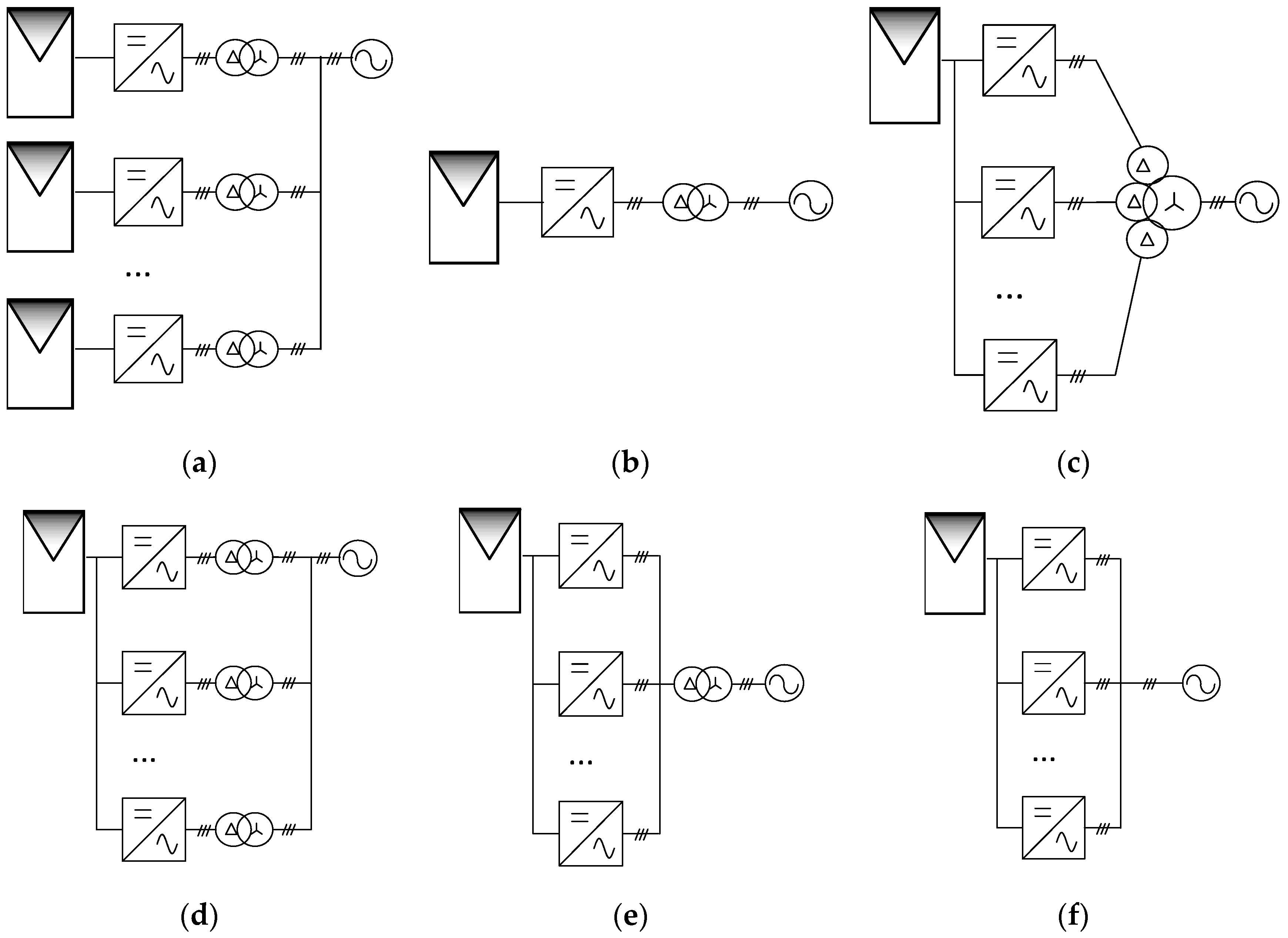
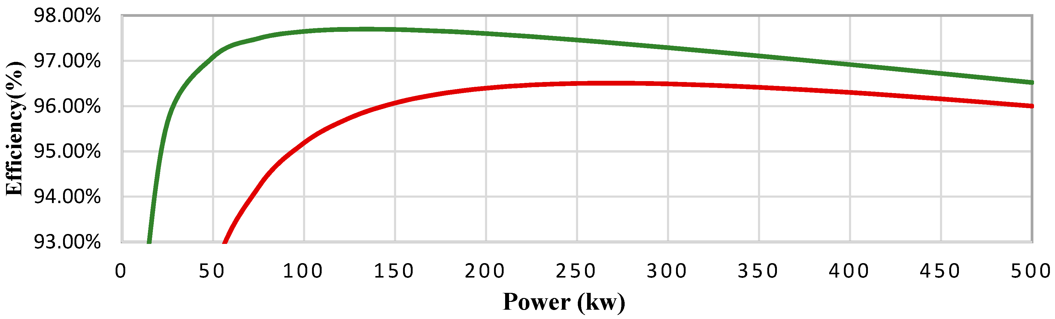
:1. Introduction
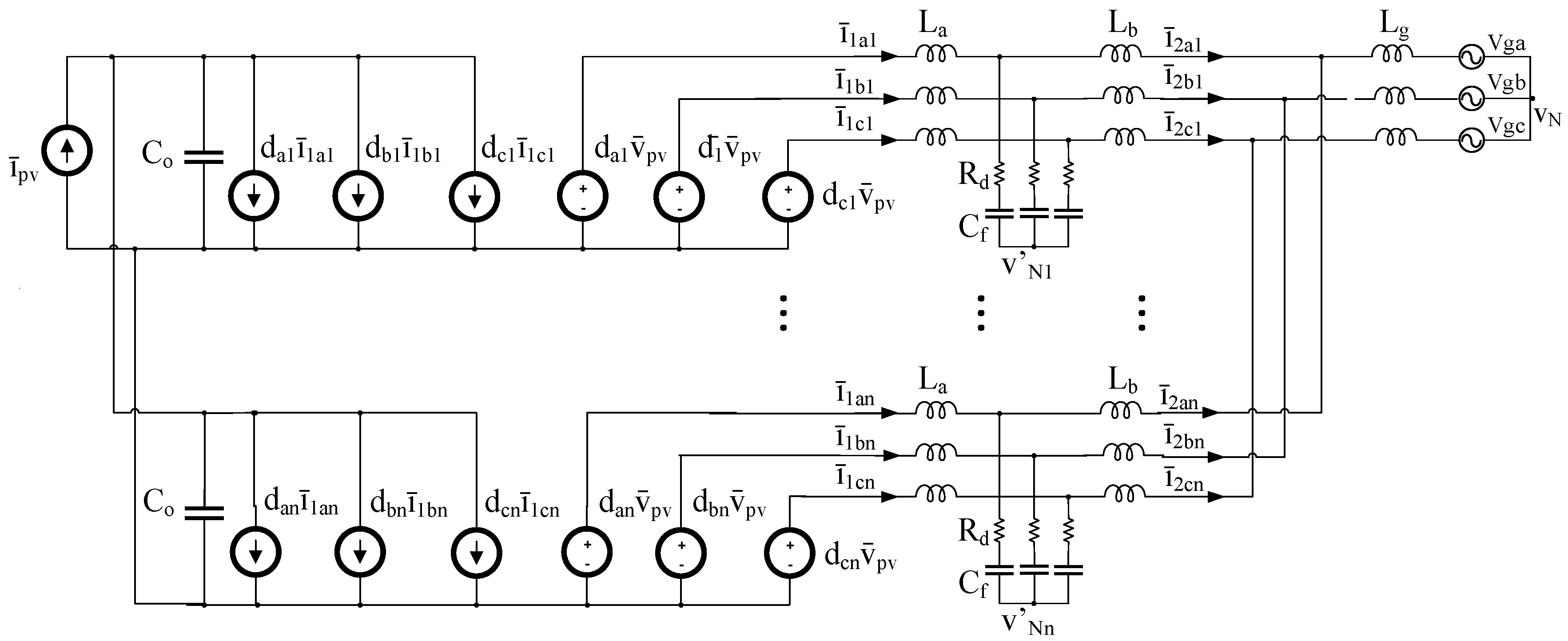
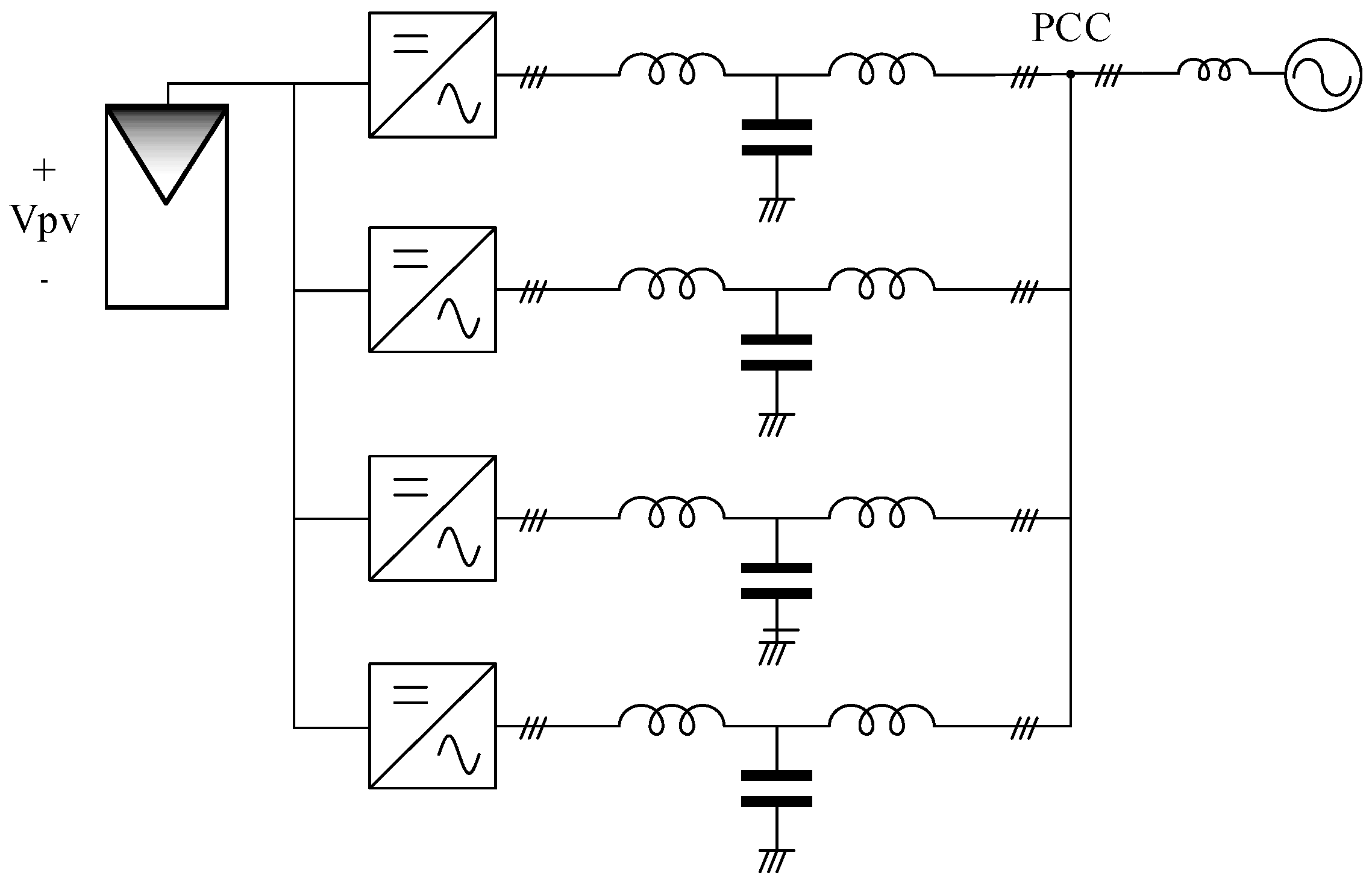
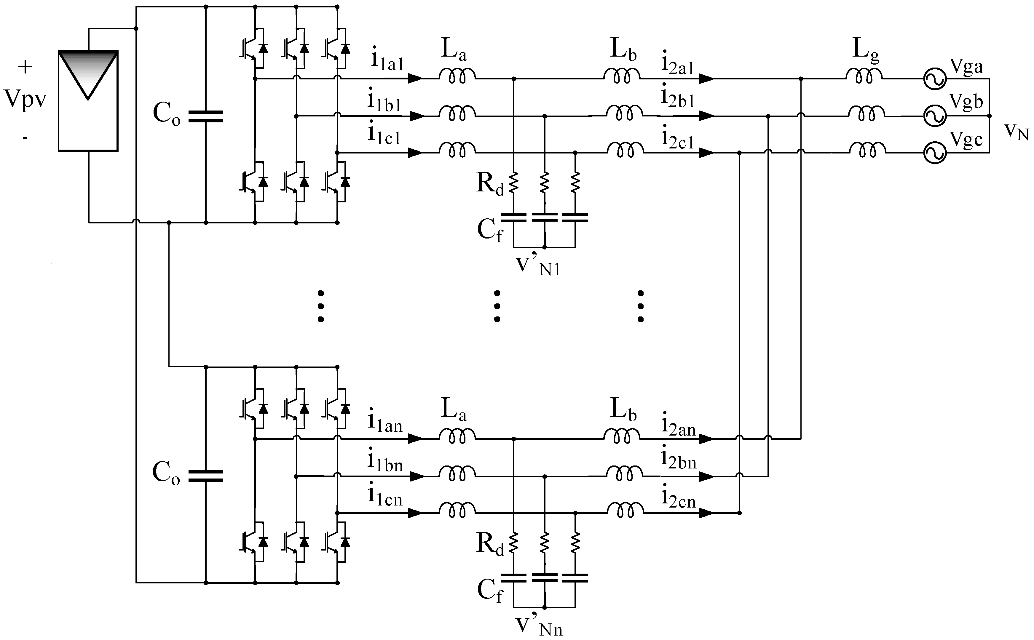
2. Modeling of n Parallel pv Inverters in a Synchronous Reference Frame
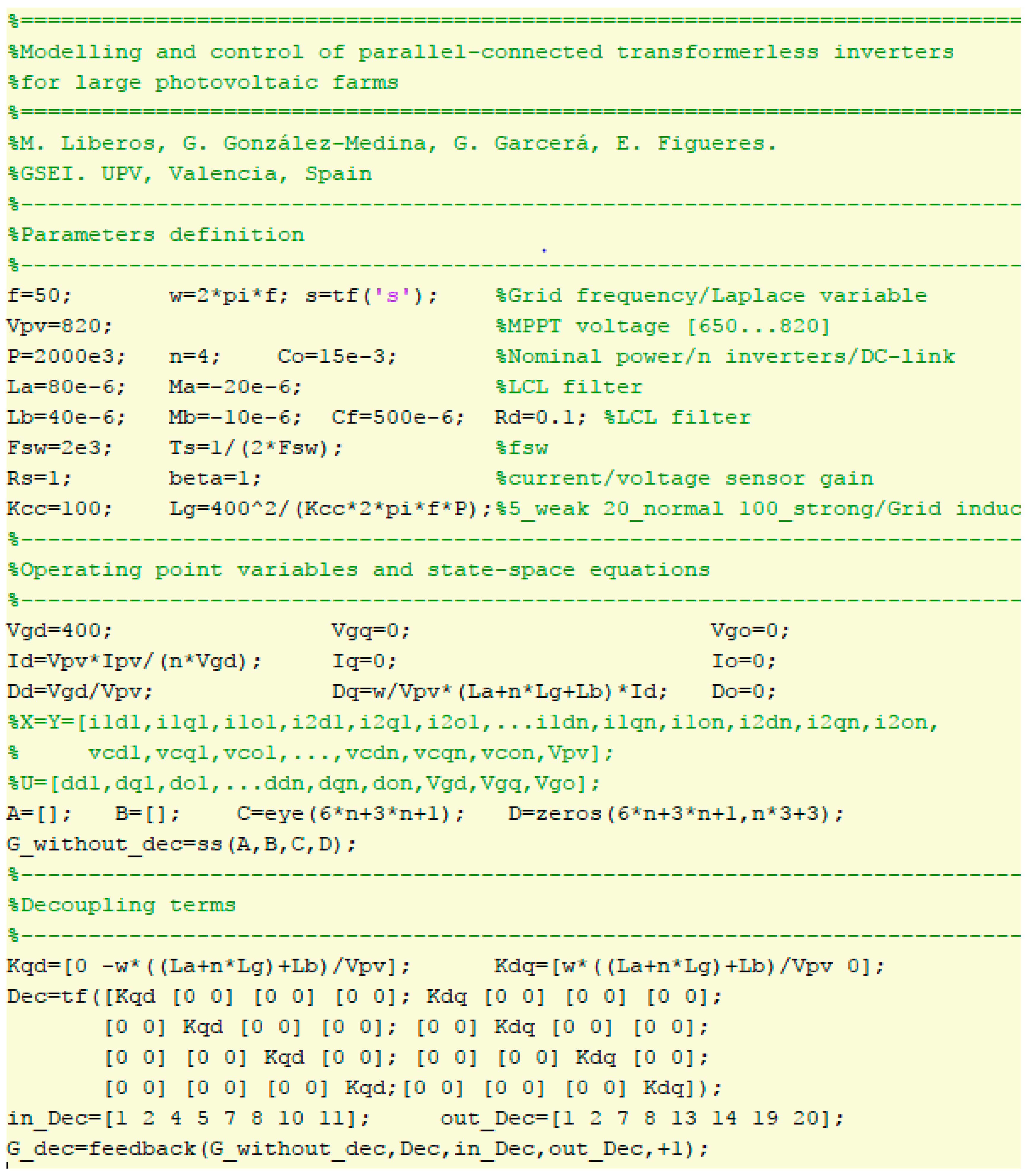
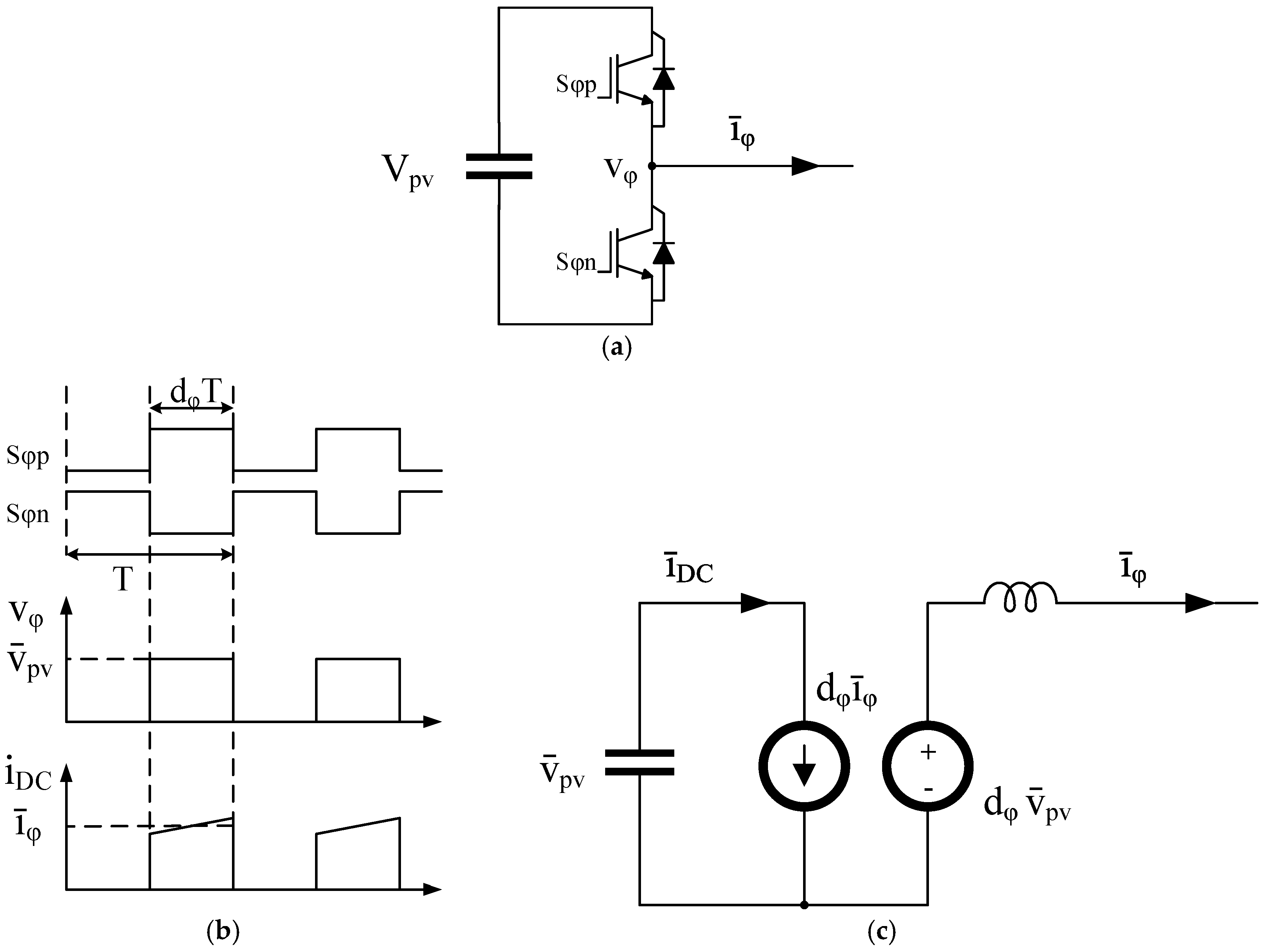
2.1. Equations of the Averaged Model
2.2. Development of the Small-Signal Model in the State Space
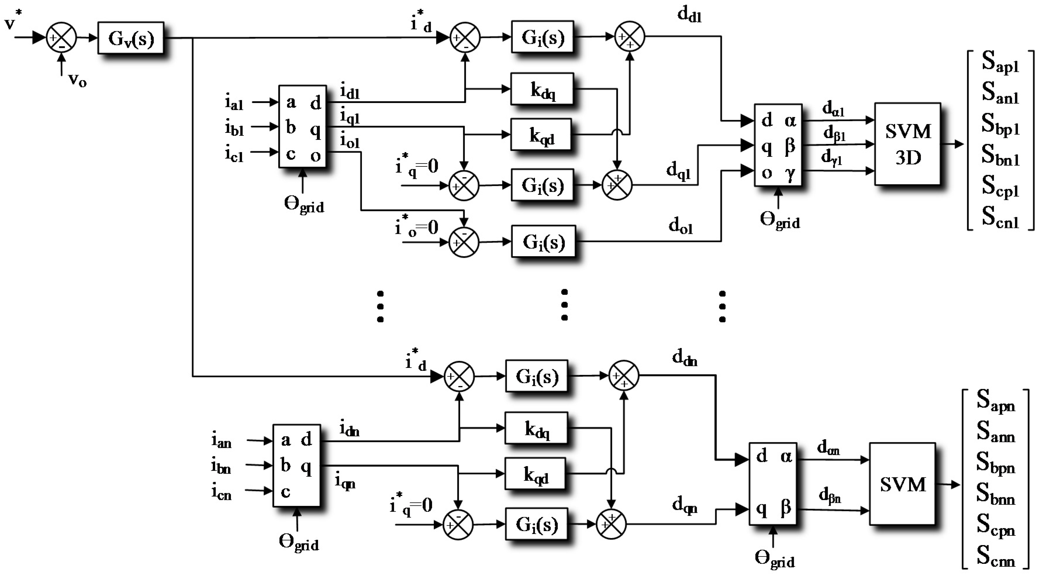
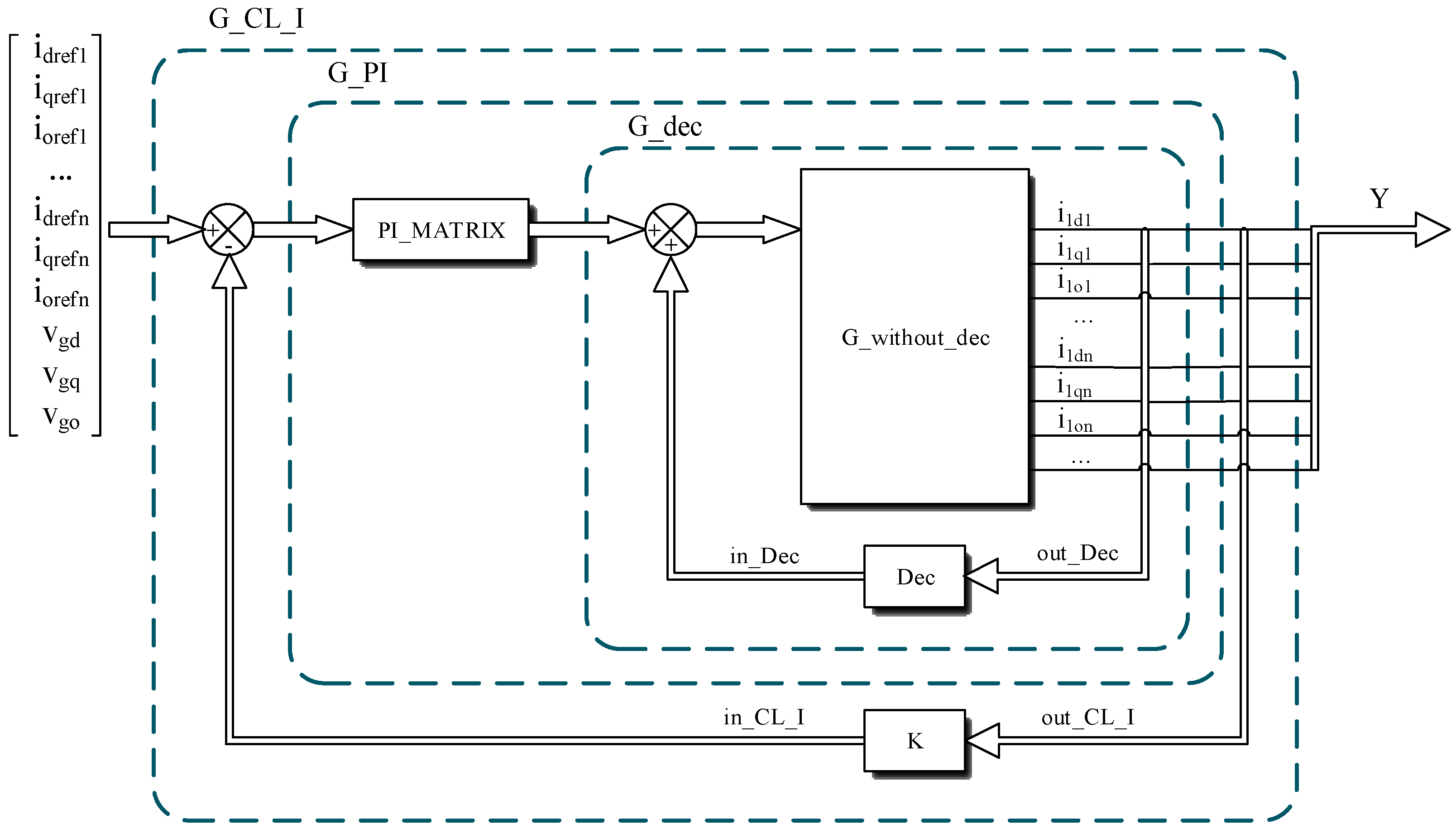
3. Description of the Proposed Control Architecture for n Parallel PV Inverters
3.1. Overview of the Control Stage
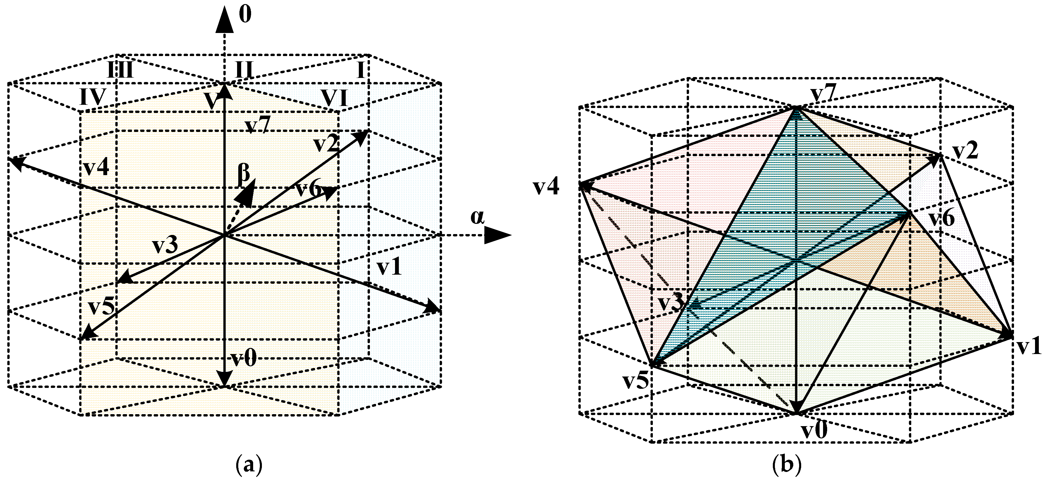
3.2. Three-Dimension Space Vector Modulator
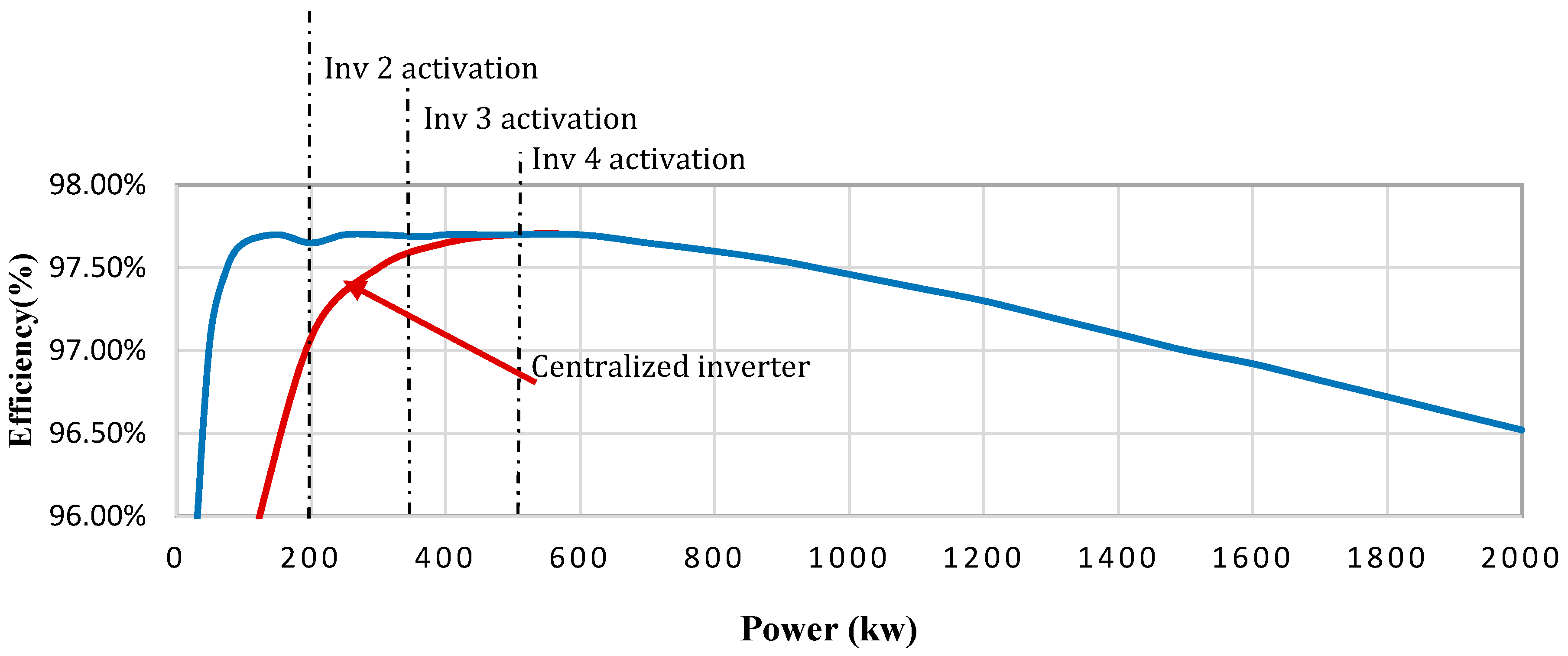
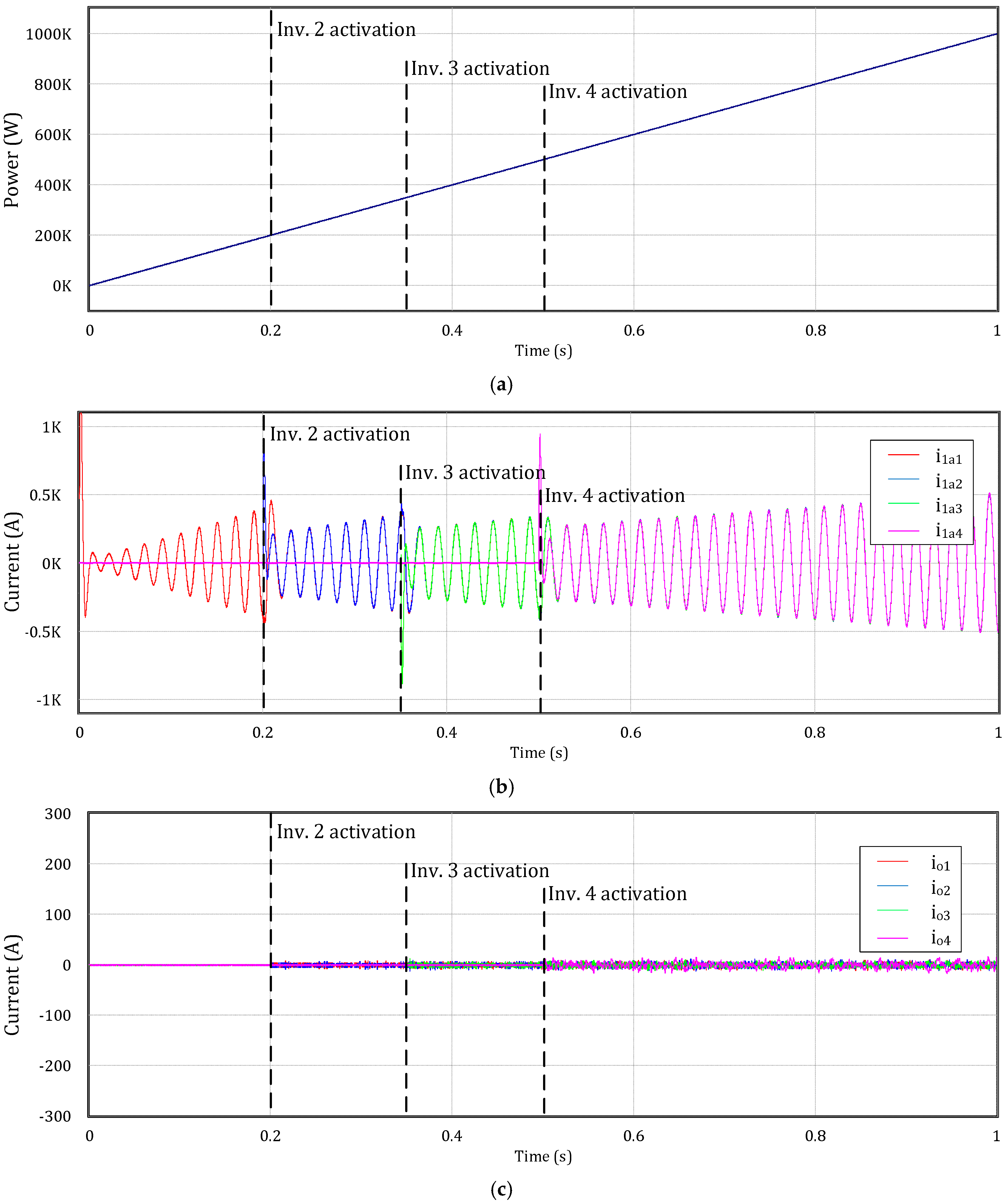
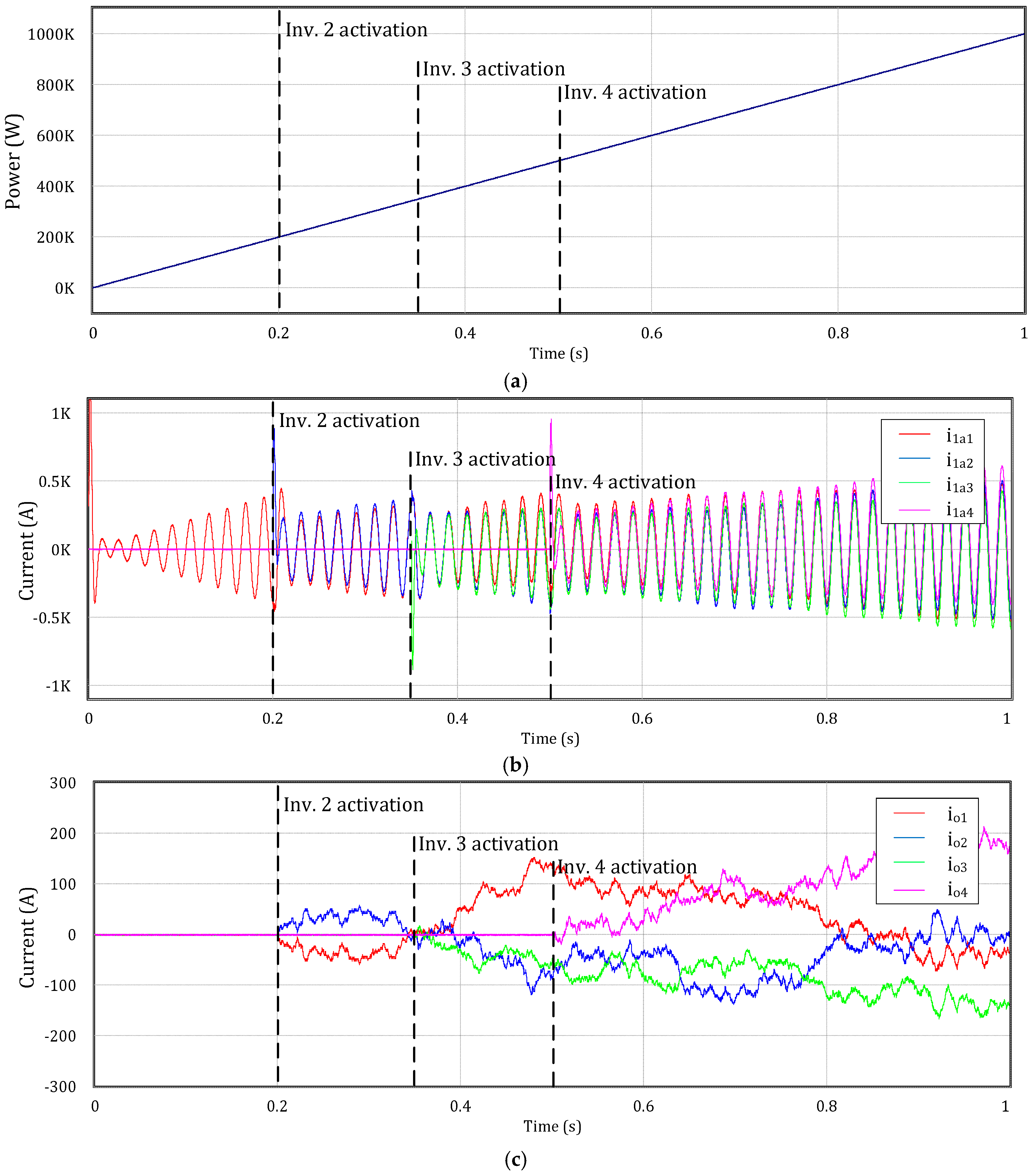
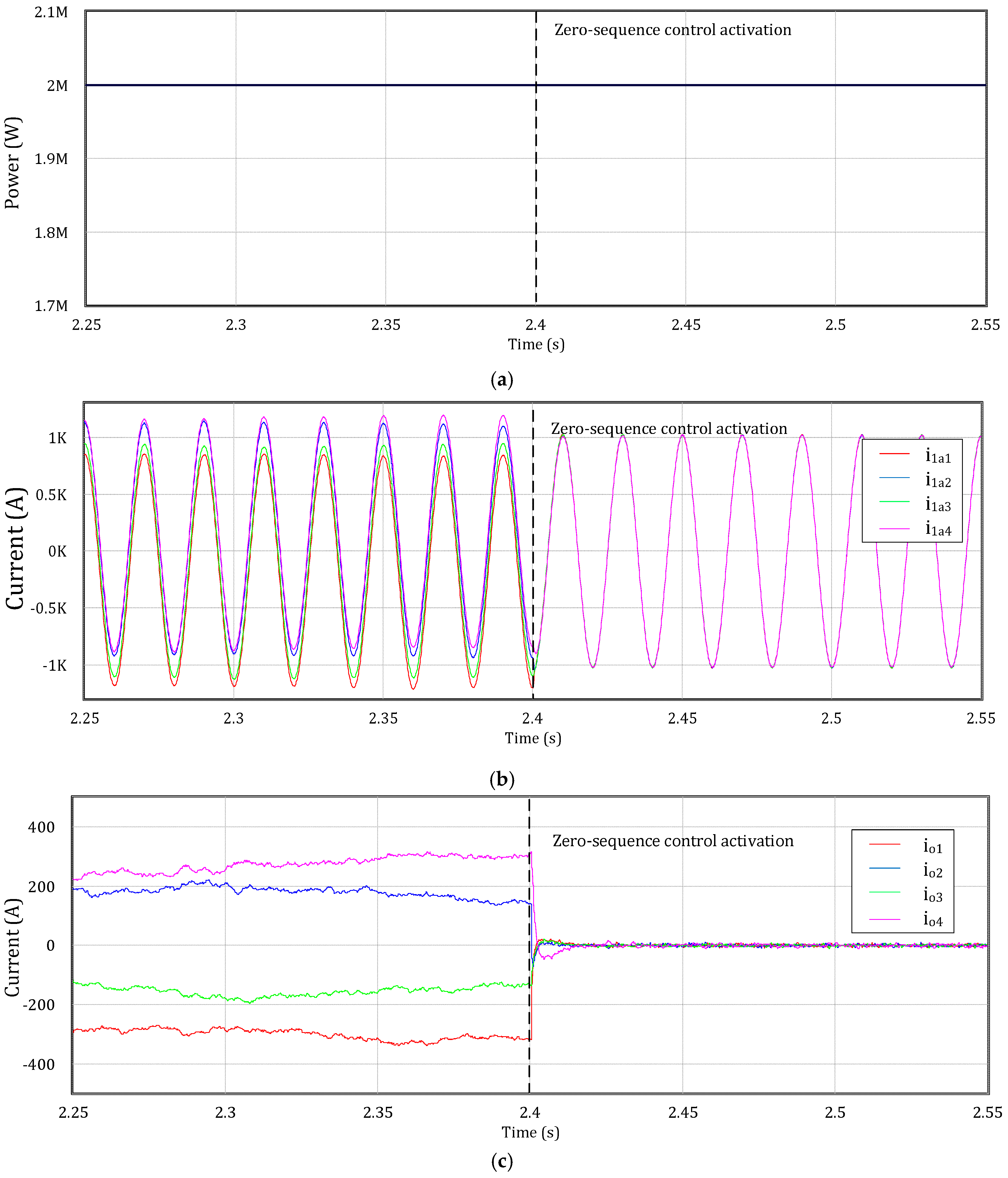
4. Application to a 2 MW PV System Composed by Four 500 kW Modules in Parallel
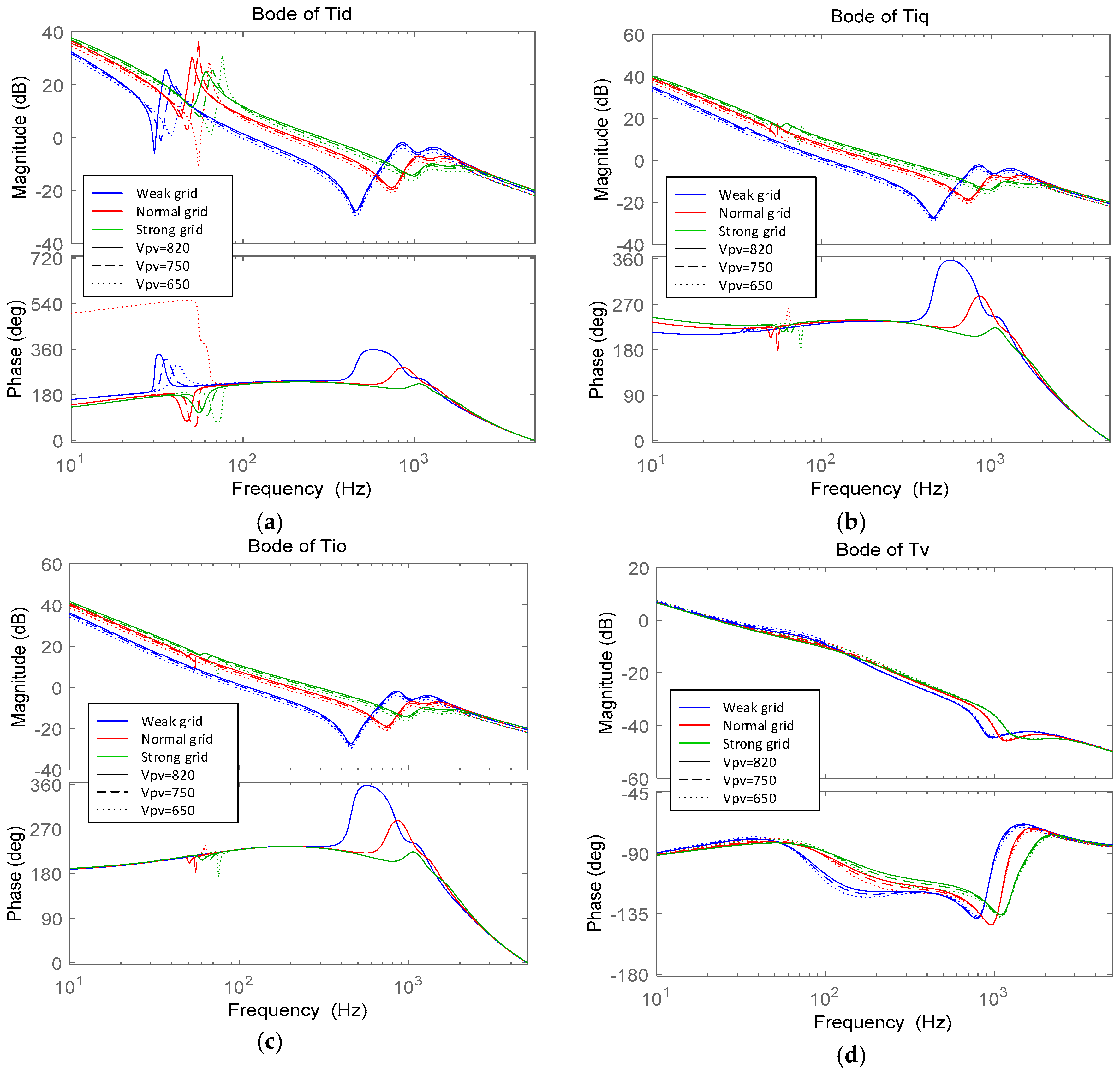
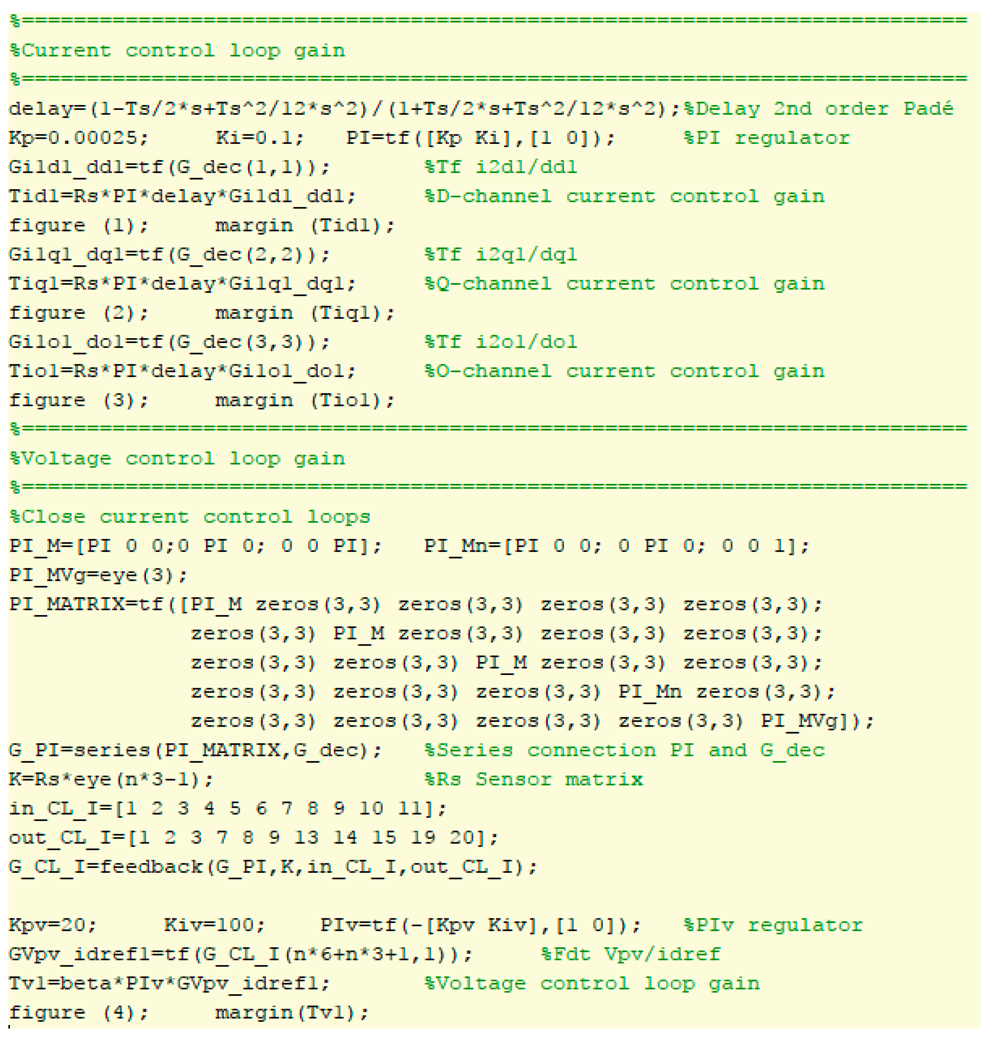
4.1. Dynamic Analysis of the Control Loops
- The crossover frequency of the current loops gain should be much higher than the fundamental frequency of the grid. In addition, it should be much lower than the switching frequency to avoid large-signal instabilities.
- The crossover frequency of the voltage loop should be much lower than the one of the current loops (typically around a factor 1/10).
- In both cases, proper stability margins (PM > 45° and GM > 6 dB) should be obtained.
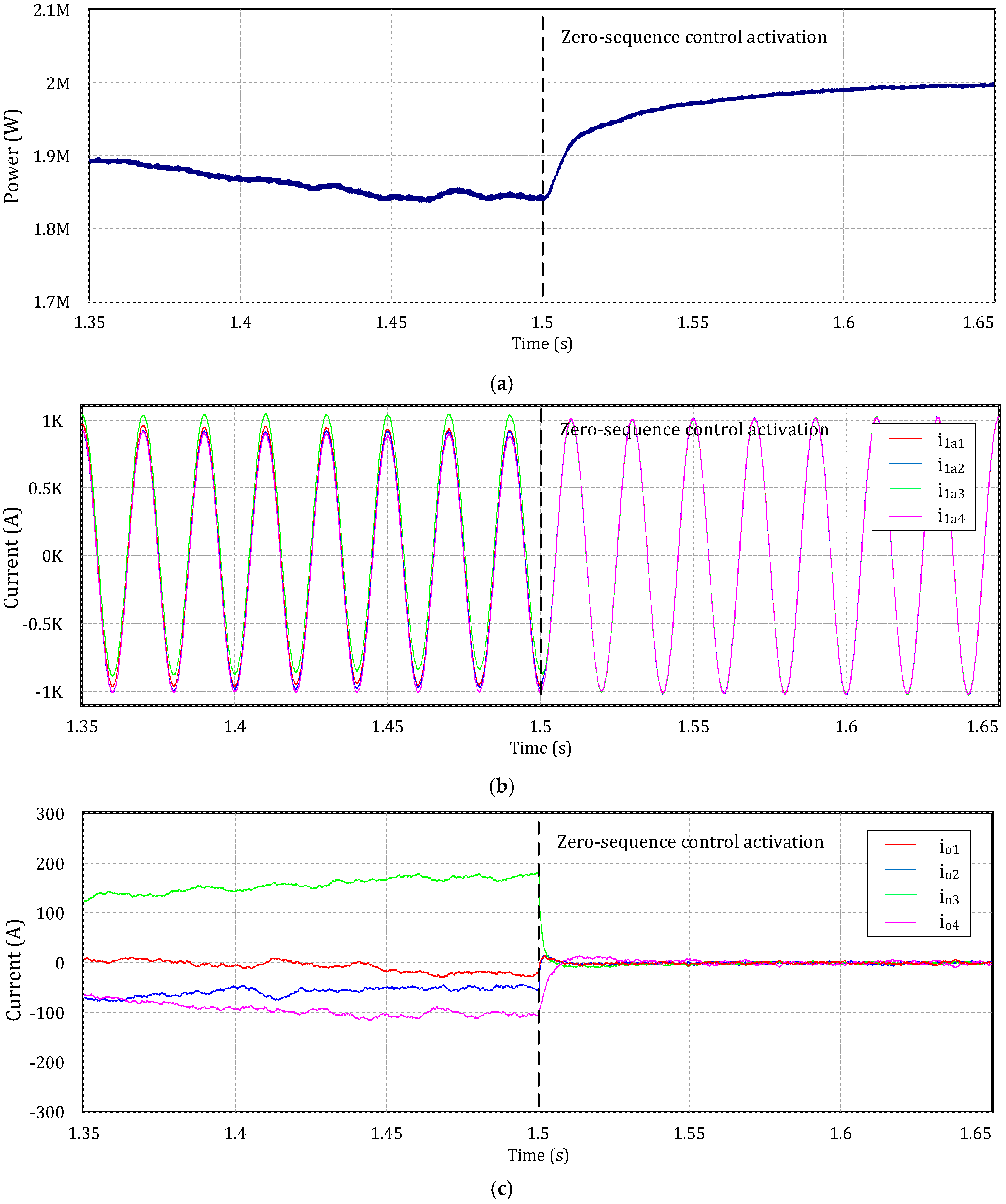
4.2. Results
5. Conclusions
Acknowledgments
Author Contributions
Conflicts of Interest
References
- Pazheri, F.R.; Othman, M.F.; Malik, N.H. A review on global renewable electricity scenario. Renew. Sustain. Energy Rev. 2014, 31, 835–845. [Google Scholar] [CrossRef]
- Subudhi, B.; Pradhan, R. A Comparative Study on Maximum Power Point Tracking Techniques for Photovoltaic Power Systems. IEEE Trans. Sustain. Energy 2013, 4, 89–98. [Google Scholar] [CrossRef]
- Borrega, M.; Marroyo, L.; González, R.; Balda, J.; Agorreta, J.L. Modeling and Control of a Master–Slave PV Inverter With N-Paralleled Inverters and Three-Phase Three-Limb Inductors. IEEE Trans. Power Electron. 2013, 28, 2842–2855. [Google Scholar] [CrossRef]
- Duman, T.; Marti, S.; Moonem, M.A.; Kader, A.A.R.A.; Krishnaswami, H. A Modular Multilevel Converter with Power Mismatch Control for Grid-Connected Photovoltaic Systems. Energies 2017, 10, 698. [Google Scholar] [CrossRef]
- Araujo, S.V.; Zacharias, P.; Mallwitz, R. Highly Efficient Single-Phase Transformerless Inverters for Grid-Connected Photovoltaic Systems. IEEE Trans. Ind. Electron. 2009, 57, 3118–3128. [Google Scholar] [CrossRef]
- Satcon, Pv Inverters. PowerGate Plus 500 kW. Available online: http://www.satcon.com (accessed on 18 August 2017).
- Agorreta, J.L.; Borrega, M.; López, J.; Marroyo, L. Modeling and Control of N-Paralleled Grid-Connected Inverters With LCL Filter Coupled Due to Grid Impedance in PV Plants. IEEE Trans. Power Electron. 2010, 26, 770–785. [Google Scholar] [CrossRef]
- Power Electronics. Available online: http://www.power-electronics.com (accessed on 18 August 2017).
- ABB, ABB Central Inverters. PVS980—1818 to 2091 kVA. Available online: http://new.abb.com (accessed on 18 August 2017).
- Infineon, Central Inverter Solutions. Available online: https://www.infineon.com/cms/en/applications/solar-energy-systems/central-inverter-solutions/ (accessed on 18 August 2017).
- Xiao, H.F.; Xie, X.J.; Chen, Y.; Huang, R.H. An optimized transformerless Photovoltaic Grid-Connected Inverter. IEEE Trans. Ind. Electron. 2011, 58, 1887–1895. [Google Scholar] [CrossRef]
- Ye, Z.; Boroyevich, D.; Lee, F. Modeling and control of zero-sequence current in parallel multi-phase converters. In Proceedings of the Power Electronics Specialists Conference, Galway, Ireland, 23–23 June 2000. [Google Scholar]
- Mazumder, S.M. A novel discrete control strategy for independent stabilization of parallel three-phase boost converters by combining space-vector modulation with variable-structure control. IEEE Trans. Power Electron. 2003, 18, 1070–1083. [Google Scholar] [CrossRef]
- Pan, C.T.; Liao, Y.H. Modeling and Control of Circulating Currents for Parallel Three-Phase Boost Rectifiers With Different Load Sharing. IEEE Trans. Ind. Electron. 2008, 55, 2776–2785. [Google Scholar]
- Ogasawara, S.; Takagaki, J.; Akagi, H.; Nabae, A. A novel control scheme of a parallel current-controlled PWM inverter. IEEE Trans. Ind. Appl. 1992, 28, 1023–1030. [Google Scholar] [CrossRef]
- Ye, Z.H.; Boroyevich, D.; Choi, J.Y.; Lee, F.C. Control of circulating current in two parallel three-phase boost rectifiers. IEEE Trans. Power Electron. 2002, 2, 609–615. [Google Scholar]
- Figueres, E.; Garcera, G.; Sandia, J.; Gonzalez-Espin, F.; Rubio, J.C. Sensitivity Study of the Dynamics of Three-Phase Photovoltaic Inverters With an LCL Grid Filter. IEEE Trans. Ind. Electron. 2009, 56, 56–706. [Google Scholar] [CrossRef]
- Figueres, E.; Garcera, G.; Sandia, J.; Gonzalez-Espin, F.; Calvo, J.; Vales, M. Dynamic Analysis of Three-phase Photovoltaic Inverters with a High Order Grid Filter. In Proceedings of the IEEE International Symposium on Industrial Electronics, Vigo, Spain, 4–7 June 2007. [Google Scholar]
- Mohd, A.; Ortjohann, E.; Hamsic, N.; Sinsukthavorn, W.; Lingemann, M.; Schmelter, A.; Morton, D. Control strategy and space vector modulation for three-leg four-wire voltage source inverters under unbalanced load conditions. IET Power Electron. 2010, 3, 323–333. [Google Scholar] [CrossRef]
- Albatran, S.; Fu, Y.; Albanna, A.; Schrader, R.; Mazzola, M. Hybrid 2D-3D Space Vector Modulation Voltage Control Algorithm for Three Phase Inverters. IEEE Trans. Sustain. Energy 2013, 4, 734–744. [Google Scholar] [CrossRef]


| Variable | Variable | Variable | |||
|---|---|---|---|---|---|
| 0 | 0 | ||||
| 0 | 0 | ||||
| 0 | |||||
| vφ | v0-000 | v1-100 | v2-110 | v3-010 | v4-011 | v5-001 | v6-101 | v7-111 |
|---|---|---|---|---|---|---|---|---|
| 0 | 0 | |||||||
| 0 | 0 | 0 | 0 | |||||
| Prism | Commutation Vectors Sequence |
|---|---|
| I | v7-v2-v1-v0-v1-v2-v7 |
| II | v7-v2-v3-v0-v3-v2-v0 |
| III | v7-v4-v3-v0-v3-v4-v7 |
| IV | v7-v4-v5-v0-v5-v4-v7 |
| V | v7-v6-v5-v0-v5-v6-v7 |
| VI | v7-v6-v1-v0-v1-v6-v7 |
| Parameter | Nominal Value | Parameter | Nominal Value |
|---|---|---|---|
| Vg-RMS (line voltage) | 230 V | Ma | −20 µH |
| Vpv (MPPT range) | [650–820] V | Mb | −10 µH |
| Vdc max | 1000 V | Cf | 500 µF |
| Pn | 500 kW | Rd | 0.1 Ω |
| Co | 15 mF | fsw | 2 kHz |
| La | 80 µH | Rs | 1 V/A |
| Lb | 40 µH | β | 1 V/V |
| Nature of the Grid | Rsc | Lg |
|---|---|---|
| Weak | 5 | 50 µH |
| Normal | 20 | 12.7 µH |
| Strong | 100 | 2.5 µH |
© 2017 by the authors. Licensee MDPI, Basel, Switzerland. This article is an open access article distributed under the terms and conditions of the Creative Commons Attribution (CC BY) license (http://creativecommons.org/licenses/by/4.0/).
Share and Cite
Liberos, M.; González-Medina, R.; Garcerá, G.; Figueres, E. Modelling and Control of Parallel-Connected Transformerless Inverters for Large Photovoltaic Farms. Energies 2017, 10, 1242. https://doi.org/10.3390/en10081242
Liberos M, González-Medina R, Garcerá G, Figueres E. Modelling and Control of Parallel-Connected Transformerless Inverters for Large Photovoltaic Farms. Energies. 2017; 10(8):1242. https://doi.org/10.3390/en10081242
Chicago/Turabian StyleLiberos, Marian, Raúl González-Medina, Gabriel Garcerá, and Emilio Figueres. 2017. "Modelling and Control of Parallel-Connected Transformerless Inverters for Large Photovoltaic Farms" Energies 10, no. 8: 1242. https://doi.org/10.3390/en10081242
APA StyleLiberos, M., González-Medina, R., Garcerá, G., & Figueres, E. (2017). Modelling and Control of Parallel-Connected Transformerless Inverters for Large Photovoltaic Farms. Energies, 10(8), 1242. https://doi.org/10.3390/en10081242