1. Introduction
Against a background where the energy crisis and environmental pollution are becoming increasingly serious, many distributed power generation technologies, such as wind power generation, photovoltaic power generation, have been rapidly developed and widely applied. However, the direct parallel operation of many distributed power generations can reduce the stability and reliability of power systems and deteriorate the power quality [
1,
2,
3]. To a certain extent, these problems can be avoided by connecting the distributed power generations in the form of micro-grids which is favored by the electric research community. The hardware-in-the-loop real-time simulation platform for micro-grids plays a very important role in the process of testing newly developed control equipment and management systems.
Micro-grids cannot work without power electronic switching devices, the switching frequency of which ranges from several kilohertz to tens of thousands of Hertz and even higher. This requires the simulation step length of micro-grid electromagnetic transients to be shortened to microseconds, or even sub-microseconds, which has challenged the real-time simulation researchers at home and abroad. The different states of time-varying elements and non-linear elements lead to different admittance inverse matrices and all the possible admittance inverse matrices value are prestored [
4], which frees one from computational pressure to solve the node voltage equation, but on the other hand it requires enough data storage space. The power electronic switching devices are modelled based on the associated discrete circuit (ADC) model [
5], which avoids the recalculation of the admittance inverse matrices due to state switching, but it reduces the simulation accuracy. The multi-port hybrid equivalent method is used to equalize the large-scale power network into multiple sub-networks [
6], which effectively enlarges the storage space problem caused by prestoring the admittance inverse matrices. The power network is decoupled by an improved latency-based approach and the sub-networks are solved by different simulation steps [
7], which can limit the small step simulation within a small bound and scale up simulation. These methods effectively promote the implementation of micro-grid real-time simulations, but the excellent hardware, such as real time digital power system simulator (RTDS), and real time lab (RT-LAB), also play a key role in the hardware-in-the-loop real-time simulation [
8,
9,
10]. Although there are big differences among the relevant software of these simulation platforms, all their core devices are either central processing unit (CPU) or digital signal processing (DSP), which targets high-speed computing. Due to the limited number of arithmetic logic elements inside the CPU or DSP, cluster methods are commonly used to solve the calculation problem of micro-grid electromagnetic transient real-time simulation. However, the establishment of a micro-grid hard-ware-in-the-loop real time simulation platform on a large scale based on RTDS or RT-LAB requires huge amounts of funding, so it is difficult to promote the real-time simulation platform to the general scientific research institutions and advanced colleges, let alone use it for technical training in the power sector.
FPGA, which has an abundant amount of logic, storage and DSP resources, can be used for power system electromagnetic transient real-time simulation. FPGA realizes real time simulation of transmission line using a full frequency-dependent modeling and conventional component model [
11]. Wang proposed a computational solution framework aimed at active distribution network based on FPGA and gave the hardware implementation of several key function modules [
12,
13]. Multi-FPGA electromagnetic transient real-time simulation is studied for large-scale power system [
14]. The hardware circuits in these references are designed on the basis of the simulation objects, which can minimize the simulation time, but this requires the programmers to have high FPGA programming capabilities and power system expertise. A real-time digital simulator based on FPGA and orders is designed and an order generator is proposed [
15], providing electrical engineers with a general beginner’s all-purpose symbolic instruction code (BASIC) programming ability so they can design new simulation applications. FO-RTDS has broken the design concept of converting the simulation object into hardware, which provides a new idea to realize the electromagnetic transient real-time simulation of power system based on FPGA.
Each input of arithmetic logic unit in FO-RTDS is equipped with a read controller and each output of arithmetic logic units is equipped with a write controller and a buffer channel. The buffer channel consists of registers which can be read and written from any position. The controller based on order can effectively improve the flexibility of arithmetic and logic operations, but it requires a large number of logical and storage resources. In the process of building FO-RTDS, the logic resources or storage resources may be used up fast, but a lot of DSP resources still remain, which makes the computing ability of FO-RTDS not be very high. Although multi-valued parameter prestorage algorithms and multi-rate simulation algorithms can effectively reduce the amount of calculation, they cannot be achieved in FO-RTDS. Directed acyclic graph (DAG) is used to describe the relationship among the computational tasks in FO-RTDS and a list scheduling algorithm that takes resource constraints into account is used to achieve task scheduling, but the data interactions between microprocessor cores need to be specified in the form of computational tasks in the simulation script. Based on the characteristics of FPGA resources and micro-grid simulation, we design a real-time solver with the ability of parallel computing, multi-valued parameter pre-storage algorithm and real-time solver of multi-rate simulation algorithm. At the same time, we propose an order generator, which has the ability of auto scheduling, following the working principle of real-time solver.
The hardware core of the simulation platform−real-time solver is described in
Section 2, focusing on the design thought of micro core, data interaction and multi-valued parameter prestorage.
Section 3 describes the software core of the simulation platform−order generator, focusing on script design, task scheduling, data scheduling and other key issues.
Section 4 presents the functional test of the real-time solver, which verifies the high efficiency of the real-time solver’s computing ability. A case is studied in
Section 4, which verifies the accuracy of the real-time solver. Some experience got in the process of designing real-time solver and order generator is given in
Section 5.
2. The Real-Time Solver
The micro-grid model can be described by a set of differential equations or algebraic equations and the simulation speed depends entirely on the simulation algorithm and the real-time solver. This article expects to integrate the parallel computing, multi-valued parameter prestorage, multi-rate simulation and other ideas into the design of real-time solver combined with the characteristics of FPGA, software-hardware conversion, and make it undertake a large-scale micro-grid hardware in-the-loop real-time simulation.
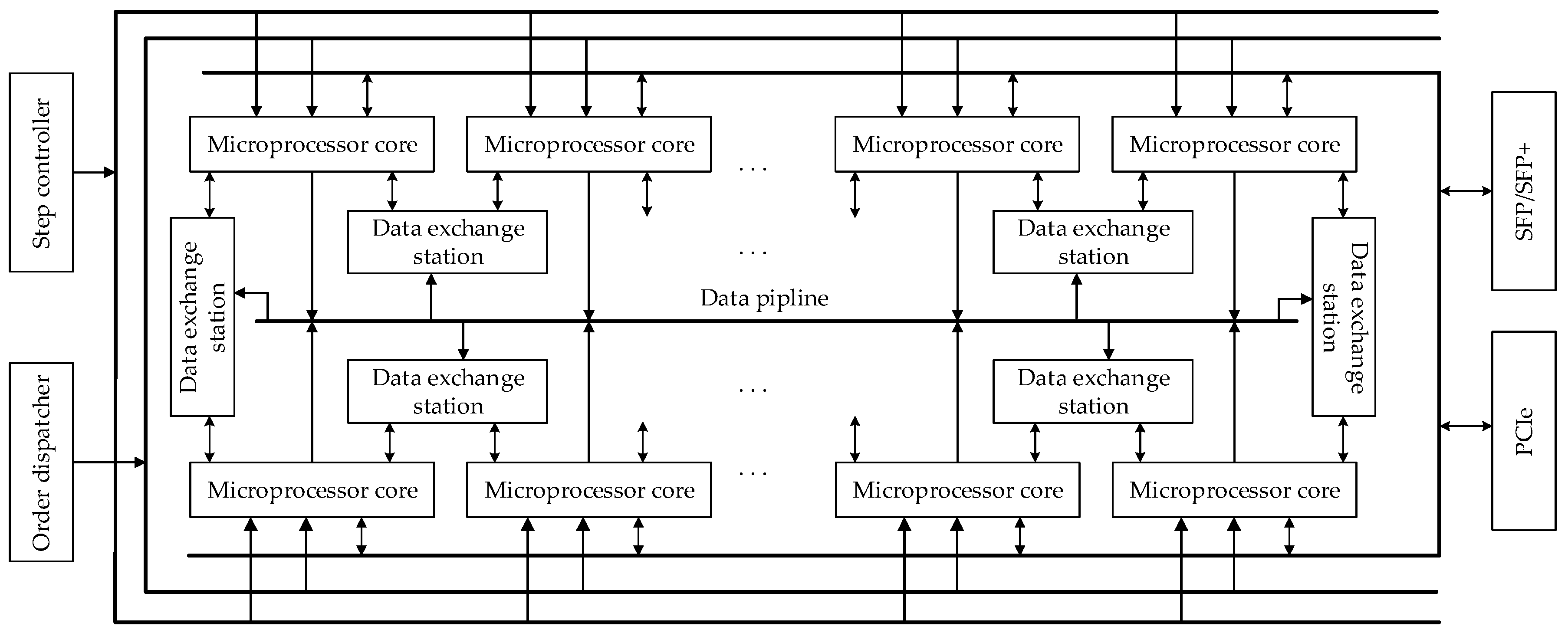
In order to avoid the phenomenon that the logic resources or storage resources are used up soon and DSP resources remain a lot, we enhance the reuse function of the Processing Element (PE) I/O and remove the order storage unit that exactly corresponds to the read/write controller which is replaced by an order dispatcher that provides service for all PEs. In order to realize multi-rate simulation and fully exert the function of microprocessor core, the interactive mode between the microprocessor core and external device is a Ping-Pong operation instead of time share operating and the rhythm is controlled by the step controller. In order to reduce the consumption of FPGA resources and maintain the data interactive abilities between micro cores, the interactive mode between data exchange stations is changed from “point-to-point” to “hand-in-hand + data-pipeline”. At the same time, the real-time solver is equipped with small form-factor pluggables (SFP)/SFP + and peripheral component interconnect express (PCIe) interface, which make it easy to connect with the digital relay protection devices, industrial control machines, input/output boards, the overall structure is shown in
Figure 1.
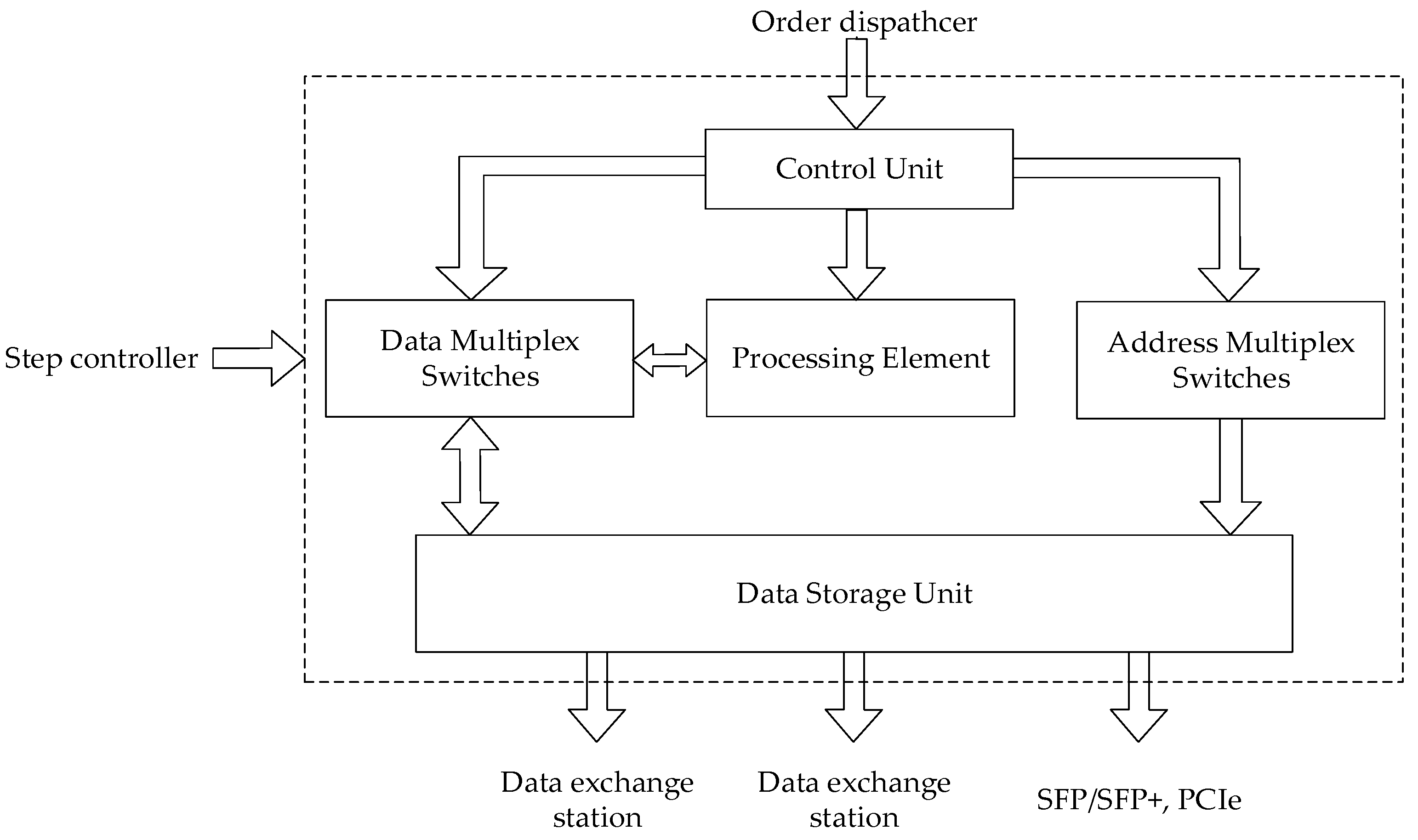
2.1. Microprocessor Core
Microprocessor cores consist of processing elements, data storage unit, control unit and multiplex switches, as shown in
Figure 2. The PEs can execute arithmetic expressions, logical expressions, and comparison expressions while the control unit, on the one hand, operates the PEs what calculations are performed on and on the other controls the status of address multiplex switches and the status of data multiplex switches to ensure that the input and output data and data storage unit are correctly connected.
With the number of PE I/O operations increasing, the number of address multiplex switches and data multiplex switches will grow dramatically, so it is necessary to increase the amount of data storage unit I/O. Therefore, the design of the microprocessor core must be weighted the advantages and the disadvantages between the scale of the PEs and the data storage unit to improve the computing ability of the real-time solver by rational utilization of FPGA resources.
2.1.1. The Processing Element
In the electromagnetic transient simulation of the power system based on the node voltage method, the arithmetic expressions can be summarized as
(the calculation of the historical current source),
(the calculation of node injection current),
(Gaussian elimination calculation),
(Gaussian generation calculation),
(current calculation) and so on.
A,
B,
C,
D,
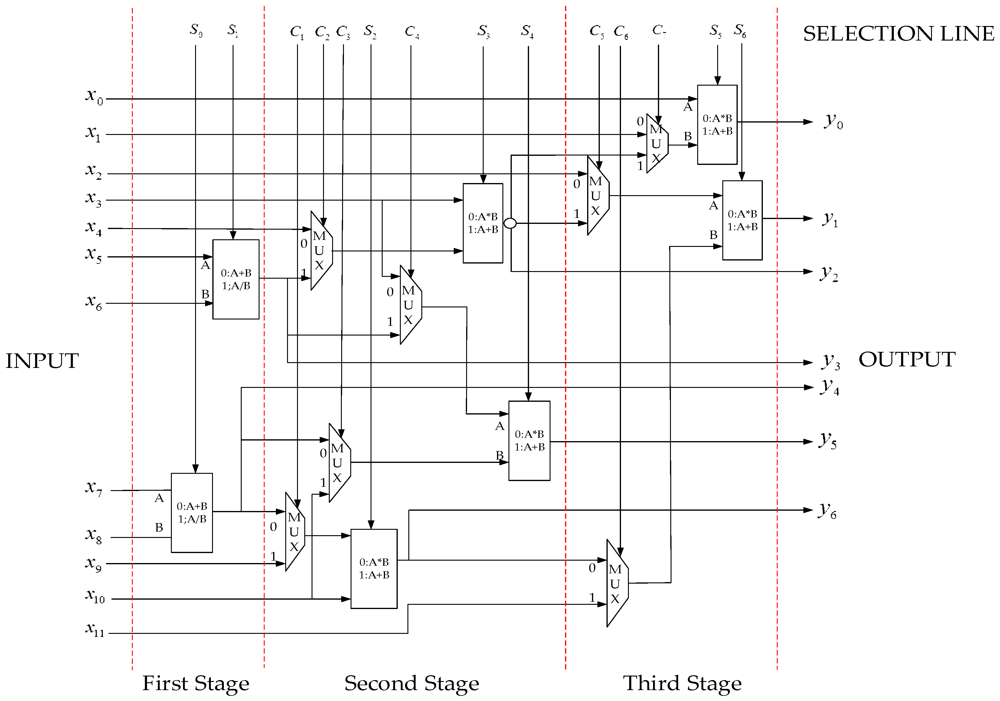
E are the corresponding calculation parameters. If specific hardware circuits are built for these arithmetic expressions, these hardware circuits are often in the idle state because of calculation process, which is undoubtedly a design method that wastes FPGA resources. In addition to the calculation of node injection current, these arithmetic expressions include three modes, namely addition-multiplication-addition, division-multiplication-addition and addition-addition-addition or just a part of one mode, they can benefit from each. In this article, the first stage calculation circuit is planned as two addition/division reuse modules, the second stage calculation circuit is planned as three addition/multiplication reuse modules, the third stage calculation circuit is planned as two addition/multiplication reuse modules and some selectors are inserted between the modules. The status of the reuse modules and selectors are controlled by the selection line.
Figure 3 shows a seven-module three-level series arithmetic expressions circuit, which executes 23 kinds of multi-input single-output arithmetic expressions.
In addition to arithmetic expressions, there are logic expressions, comparison expressions and other functions. According to the design idea of the arithmetic expression circuits, comparatively complicated logic expression circuits, comparison expression circuits and function circuits are constructed in the PEs. Multiple data direct transmission channels are constructed in the PEs. In order to allow data to migrate between data storage units, several data direct transmission channels are constructed in the PEs. As the using frequency of logic expression circuits, comparison expression circuits and function circuits are not high, the input ports of PEs are directly shared by arithmetic expression circuits, comparison expression circuits, function circuits and data transmission channels while the output ports of PEs are shared by logic expression circuits, comparison expression circuits through selectors. In this way drastically reduces the number of PE I/O while the computational function of the PEs is not affected.
2.1.2. The Data Storage Unit
Building the data storage units with registers can prevent data read-write conflicts, but FPGA logic resources cannot afford such a huge amount of data storage. Double-port block RAMs (DBRAM) are usually adopted as the data storage units in actual projects.
In order to make full use of FPGA storage resources and facilitate the data exchange with external devices, the data storage units are divided into real data inflow area, real data outflow area, real data blocking area, logical data inflow area, logical data outflow area and logical data blocking area. The inflow area stores the data that can be changed by outside, such as the node admittance matrix value, the initial power value, light intensity, temperature and so on. The outflow area stores the data that needs to be output, such as the node voltage and current. The blocking area stores the data to be used later, such as the voltage and current calculated in the previous step. Obviously, the real data inflow area is connected to the real data input of the PEs; the real data outflow area is connected to the real data output of the PEs; the real data blocking area is connected to the real data I/O of the PEs; the logical data inflow area is connected to the logical data input of the PEs; the logical data outflow area is connected to the logical data output of the PEs; the logical data blocking area is connected to the logical data I/O of the PEs.
The number of data storage units I/O should be estimated by the most complex expression combinations. However, since the using frequency of the inflow and outflow area is relatively low, their numbers of I/O may be less than estimates.
2.1.3. The Control Unit
Although the reuse of I/O is taken into account in the design of the PEs, many I/O are still often in the idle state. In order to shorten the order length, the microprocessor core orders are described as the unequal length format like “length + code + address table” where the code gives the status word of PE I/O (the idle state is represented by 0 and the operating state is represented by 1) and the selection word of the selection line, the address table gives the address of data storage units which will be connected to the I/O in an operating state. Since the distributed order cannot guarantee that the order storage space can be made full use, the orders are aggregated to a real-time solver order as the format like: “Length + Microprocessor core order length + Microprocessor core order Code + Microprocessor core order address table”. The real-time solver orders are stored in the order dispatcher, which decomposes and reorganizes the orders and then distributes the orders to the control units of each microprocessor core.
The control unit of the microprocessor core contains a read controller, a write controller and a selection controller. These controllers have a number of buffer queues that correspond to the number of input ports, output ports and selection lines, respectively. The control unit will write data to the write buffer queue and read data from the read buffer queue at each clock. The written data is determined by the microprocessor core order. The address got in the address table is written to the buffer queue corresponding to the PE I/O in operating state. The default address is written to the buffer queue corresponding to the PE I/O in idle state. The code is written to the buffer queue corresponding to the selection line. The data read from the write buffer queue and the data written to the write buffer queue is the address of the data storage unit associated with PE I/O. The data read from control buffer queue is the state of the reuse modules and the selector.
In order to ensure that the PEs work in a good order, the length of these buffer must be consistent with the input and output pipeline length of the reuse modules and the buffer corresponding to the selection line should be the same as the output line of the reuse modules. The length of the buffer queue corresponding to the reuse modules selection port line should be in line with the output line length of the reuse modules.
2.2. Data Interaction
2.2.1. The Interaction between Microprocessor Cores and External Devices
The data inflow area and the data outflow area of the data storage units are used less frequently, so for communication circuit one part of time shall be used in PEs and the other time in external devices. However, this time-sharing mechanism has constrained the arrangement of calculation task, which will not make full use of the microprocessor core.
In this article, there are two sets of the data inflow area and the data outflow area of the data storage unit, one for PEs and another for communication circuits according to the simulation step. This Ping-Pong mechanism consumes more FPGA storage resources, but it lifts the read/write restrictions of the data inflow area and the data outflow area.
For the data inflow areas and the data outflow areas, if a portion of their read/write ports are dedicated to the PEs and the others to the communication circuits, the PEs and the communication circuits will have different operating frequencies, but this will reduce the data transmission ability between the PEs and the data inflow/outflow areas. The first in first out (FIFO) circuits are added between the communication circuits and the data inflow areas as well as between the PEs and the data outflow areas in this article so that the PEs and the communication circuits will have different operating frequencies and maintain the data transmission capacity between the PEs and the data inflow/outflow areas.
The PEs can write the complete output data to the data outflow area at regular time, but the communication circuits cannot write the complete input data to the data inflow area at regular time and it just tells which input data has been changed. In order to update the input data of the data inflow area, the FIFO circuits between the communication circuits and the data inflow area are changed into two sets, and the read/write ports of the data inflow area are fixedly jointed to the read ports of the FIFO circuits. The communication circuits write data to the two sets of FIFO circuits at the same time and the FIFO circuits write the data to the data inflow area according to the simulation step.
Since the order dispatcher is responsible for issuing the orders to the microprocessor core, the repetition period of the order for each microprocessor core depends entirely on the restart period of the order dispatcher. This period is generally consistent with the maximum simulation step. In order to realize multi-rate real-time simulation, there should be multiple data inflow areas and data outflow areas of each microprocessor core, the number of which is equal to that of simulation steps and the interaction period of which corresponds to the simulation step.
2.2.2. The Interaction between Microprocessor Cores
For each microprocessor core, there is a data exchange station, the owner of which is readable and the other microprocessors only have the right to write. This point-to-point data interaction will consume a large number of FPGA logic resources when the real-time solver has many microprocessor cores.
Each microprocessor core can read and write to two data exchange stations in this article and each data exchange station is only read and written by two microprocessor cores. The hand-in-hand interactive mode will maintain the interactive ability between the adjacent microprocessor cores and will not increase the microprocessor core at the expenses of FPGA logic resources. However, the data exchange between remote microprocessors need to be solved by multiple data exchange stations, which not only increases the data interaction latency, but also decreases the computing ability of relevant microprocessor cores.
To solve the problem of data interaction between remote microprocessors, several data-pipelines are built between the microprocessor core and the data exchange station. The data-pipeline consists of several data receiving FIFO circuits and a data distributing FIFO circuit. The microprocessor core sends data to the data receiving FIFO circuits. The data distributing FIFO circuit, on the one hand, reads data from the data receiving FIFO circuits and on the other distributes the data to the data exchange stations. Since the distribution is performed automatically, the data in the data-pipeline should contain the information of the data exchange stations and its data storage unit. In general, the data-pipeline ensures that data interaction between remote microprocessors are completed within three clocks. This data interactive mode is the point-to-point data interaction between the microprocessor core and the data-pipeline plus the point-to-point data interaction between the data-pipeline and the data exchange station. As there are few data-pipelines, the FPGA logic resources will not surge due to the increase of microprocessor core. Therefore, the “hand-in-hand + data-pipeline” data interactive mode can take into account both the FPGA logic resources and data exchange capacity.
2.3. Multi-Valued Parameter Prestorage
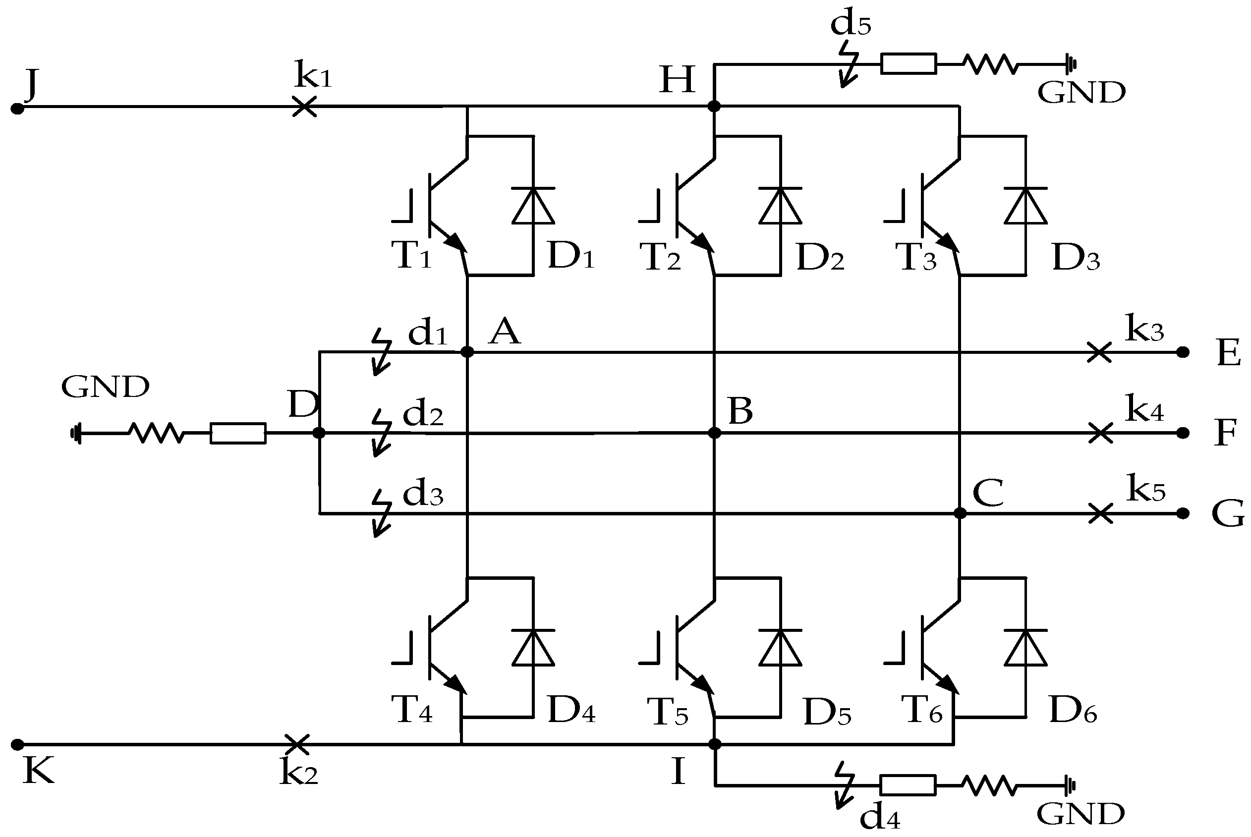
The free-wheeling diode, insulated gate bipolar transistor (IGBT), open/short circuit point in
Figure 4 can be represented by a binary resistance element, but the reasons for the change of resistance value are different. The free-wheeling diode, the resistance value of which depends on the voltage across it, is a non-linear element; the resistance value of the IGBT is controlled by the inverter controller, the resistance value of the open/circuit point is man-made, which are time-varying elements. In order to reflect the switching characteristics of the binary resistance element and to ensure the connectivity of the topology, the admittance value of the short-circuit point is defined as 10
−6 S and 10
6 S, and that of the free-wheeling diode, IGBT and the open point is 0 S and 10
6 S. The former is called the vertical switch and the latter is called the horizontal switch.
As the resistance value of the binary resistance element changes, the value of the parameters such as the equivalent conductance in the node voltage equation and the tributary current calculation formula may also change. When the influence surface of the binary resistance element is large, the time required for the calculation of parameters such as admittance matrix and equivalent conductance will be related to the problem that whether the real-time simulation will realize in short-step. In this article, parameters which have a variety of deterministic values are called multi-valued parameters in this article and their possible values are stored in the data storage unit of microprocessor core in advance.
Factors that affect the value of a multi-valued parameter are described by the influencing words. The influencing words of the self-admittance of node A in
Figure 4 include T1, D1, T4, D4, d1, k3, and the influencing words of the self-admittance of node H include T1, D1, T2, D2, T3, D3, d5, K1. Obviously, the contents of the influencing words contain both non-linear elements and time-varying elements. Because of the different properties of time-varying elements and non-linear elements, the influencing words are divided into time-varying one and non-linear one and the former one is used to store the time-varying component states while the latter for the non-linear component states. In order to realize multi-rate real-time simulation, the time-varying influencing words are divided into fast one and slow one.
If the parameters are prestored using the influencing word as offset, there will be a number of storage units with the same value. Since all vertical switches share a set of resistance values while all horizontal switches share another ones, the multi-valued parameter such as admittance can be described by the number of closed vertical switches and the number of closed horizontal switches. Therefore, it is necessary to convert the influencing word into an offset by different decoding methods. The same type of switches should be put together in the organization of influencing words in order to make it easy to decode.
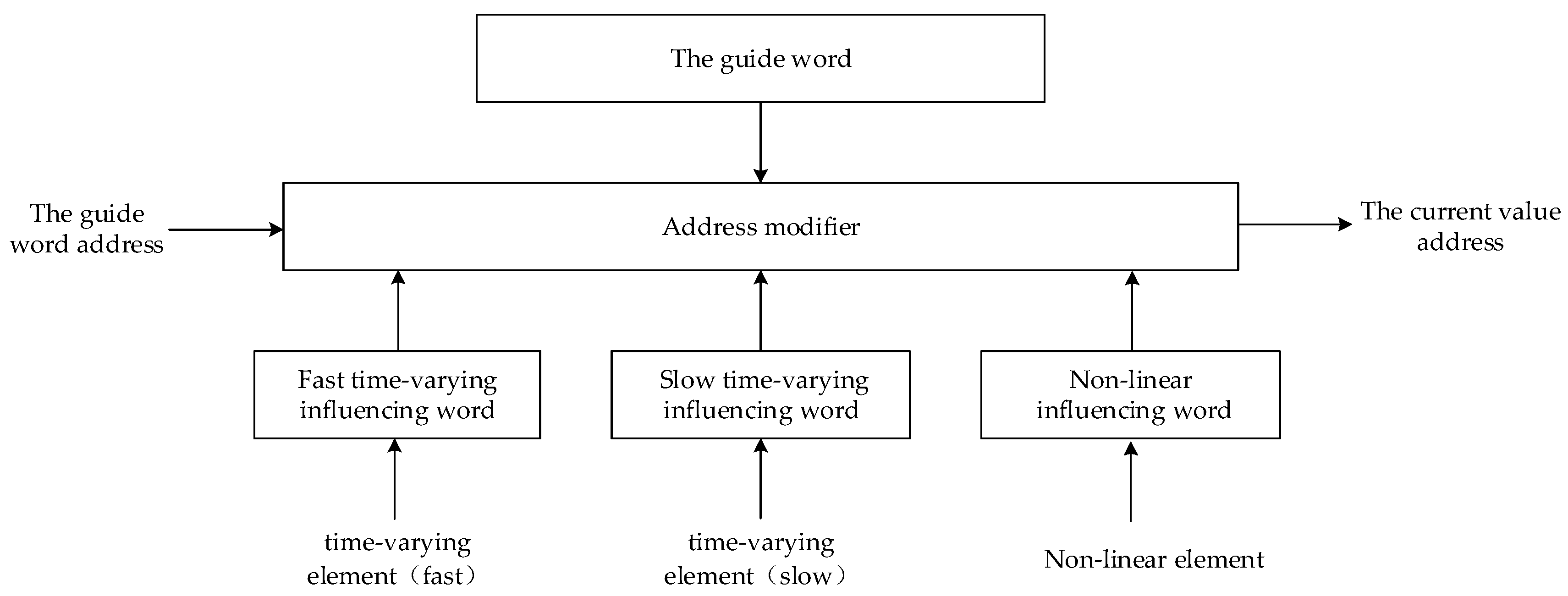
The multi-valued parameter values are stored in the data inflow area according to a certain rule. Finding the current value of the multi-valued parameter will influence the base address, the influencing words and the decoding mode. Since the influencing words need to be stored separately, the guide word of the multi-valued parameter is defined as the base address, the address of the non-linear influencing word, the address of the fast time-varying influencing word, the address of the slow time-varying influencing word and the decoding method. The given address table in the microprocessor core order is the guide word address of the multi-valued parameter.
Figure 5 is the mapping circuit converting the guide word address to the current value address. The guide word can be obtained according to the address table in the microprocessor core order, then we obtain the address of the non-linear influencing word and the address of the fast time-varying influencing word and the address of the slow time-varying influencing word according to the influencing word and the integrated influencing word can be obtained by or operation of them. The influencing word is converted into an offset according to the decoding method specified in the guide word and the offset value plus the base address in the guide word is the current value address.
3. The Order Generator
3.1. The Script Design
The PE has the function of calculating multi-input and multi-output expressions, which can be used to organize the calculation task. However, determining what principles should be followed to organize this kind of computing task is still a challenge. Therefore, this article organizes the computational tasks according to the multi-input single-output function of PE.
In the simulation algorithm, it is possible to face an expression that cannot be expressed by the PEs directly. To solve this problem, we introduce intermediate variable, mixed operations including logical variable and real number variable and Taylor series.
There are eight zones in the data storage unit of microprocessor core (the data inflow area and the data outflow area each have two sets, fast one and slow one), which area the variables are stored in should be specified in the simulation script. If the variable in the expression is a multi-valued parameter, it is also necessary to provide a guide word. If the on-off state of the IGBT and the free-wheeling diode in
Figure 5 is given by the microprocessor core, it is necessary to specify which equations affect the non-linear influencing word and which ones affect the time-varying influencing word. Besides, the voltage and current used to calculate the historical current source is the result of the previous simulation step, but the intermediate variable in the Gaussian elimination process is only used in the current simulation step. From the perspective of the real-time solver hardware structure and to facilitate the calculation of task scheduling, the variables are divided into fast multi-valued parameters, slow multi-valued parameters, fast real-number inflow variables, slow real-number inflow variables, fast real-number outflow variables, slow real-number outflow variables, real-number circulation variables, real-number intermediate variables, logical circulation variables, logical intermediate variables, logical non-linear outflow variables, fast logical time-varying outflow variables, slow logical time-varying outflow variables and so on.
The dependency relationships of the computational tasks in the simulation script are determined by the relationships between the variables. However, this cannot reflect the effects of the non-linear influencing word on multi-valued parameters. In order to describe this dependency relationships, a non-linear operational task is introduced. The input is the influencing factor and the output is the multi-valued parameters.
Multi-valued parameters, real-number inflow variables, real-number outflow variables and logical time-varying outflow variables are performed via Ping-Pong operations. Since the multi-rate simulation script is designed on the basis of the large simulation step, the Ping-Pong operations are carried out in the data inflow area and the data outflow area in the large simulation step. In order to describe this Ping-Pong operation, an inflow operation task and an outflow operation task with a time stamp are introduced. The output of the inflow operation task is inflow variables and there is no input of the inflow operation task. The input of the outflow operation task is outflow variables and there is no output of the outflow operation task.
3.2. Computational Tasks Scheduling
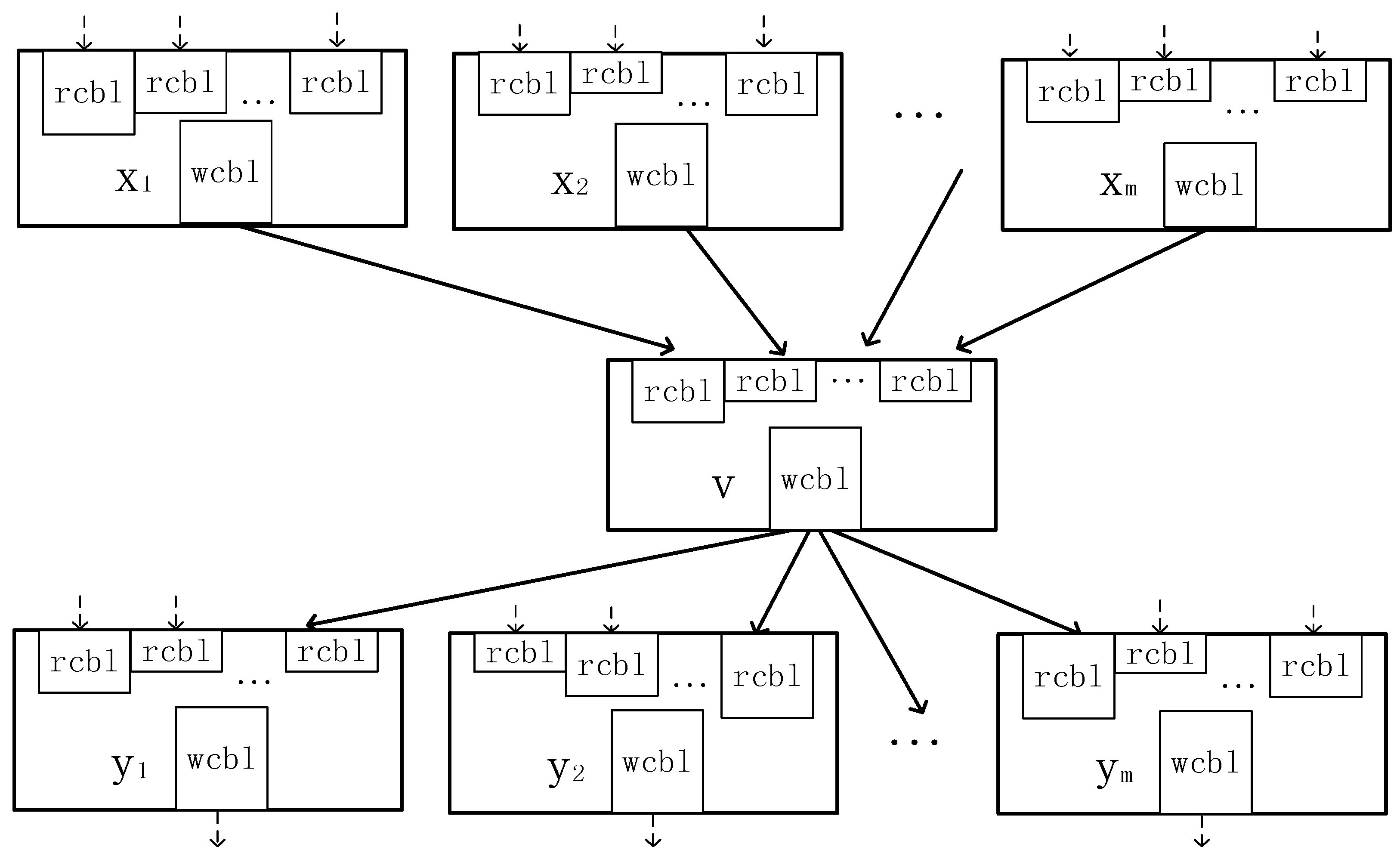
In order to facilitate task scheduling, directed acyclic graph (DAG) is used to describe the task dependency relationships in the simulation script. From the real-time solver hardware structure, we can know that the input data address and the output data address of the calculation task are written to the buffer queues at the same time. However, because of the different length of the buffer queue, the time of reading the input data and writing the output data is different. In order to describe the task with the length of the buffer queue, the length of the buffer queue for the non-linear operation task, the inflow operation task and the outflow operation task is zero.
Figure 6 shows the DAG describing the task with the buffer queue length where rcbl represents the length of read controller buffer queue and wcbl represents the length of write controller buffer queue.
What concerns most in task scheduling is the latest scheduled time (
lst) and the earliest scheduled time (
est). The
lst and the
est of the inflow operation task and the outflow operation task is preset in the simulation script but the
lst and the
est of other task need to be calculated:
where
yi is the subsequent task of
v,
lst(
yi) is the
lst of
yi,
wcbl(
v) is the length of output buffer queue,
rcbl(
yi, v) is the length of input buffer queue associated with task
v and
yi.
indicates that the subsequent task must be arranged later than the previous one. When there is no subsequent task for v, lst(yi) is equal to the large simulation step ΔT, rcbl(yi, v) = 0.
If the task
v’s previous task
x is not scheduled, it is meaningless to discuss the
est of the task
v. When the task
x is scheduled, the
est of task
v is:
rpst(xi) is the scheduling time for task xi, wcbl(xi) is the length of output buffer queue, rcbb(v,xi) is the length of input buffer queue associated with task v and xi.
also indicates that the subsequent task must be arranged later than the previous one. When there is no subsequent task for v, rst(v).
If the est of a task is less than or equal to the current execution time, the task is called a ready task. Although there are many PEs and a PE can take multiple tasks at the same time, we still cannot meet the requirements of the ready task, that is, many ready tasks cannot be immediately scheduled. If the lst for a task is less than the current execution time, the simulation script cannot be finished in the specified simulation step. Therefore, the strategy of prioritizing the lst is adopted in this article, that is, the earlier the lst, the sooner scheduled.
3.3. Data Scheduling
There are three concerns to consider during the scheduling tasks: (1) Whether the PE has input and output ports and the selection lines to undertake the task; (2) Whether the input data is in the data storage units or the data exchange stations which are associated with the inputs; (3) Whether the relevant data storage units can be read or written. When (2) and (3) cannot be met, the data can be adjusted in advance to solve the problem, but such data scheduling may consume some data to transfer channel resources of the PEs directly. To arrange the tasks orderly, the three batches task scheduling strategy is adopted. The first batch arranges the ready task which does not need to do data scheduling, the second batch arranges the ready task which meet the conditions (1,2) and the third batch arranges the ready task that only satisfies the condition (1). Definitely, the ready task must line up followed by the strategy of prioritizing the lst.
Data scheduling occurs within the microprocessor core during the second batch of the task scheduling. There are three kinds of data scheduling methods: (1) Move the data directly to the appropriate data storage unit; (2) Arrange the data to the input of the PE in advance; (3) Copy the data to the appropriate data storage unit. Method (1) adjusts the data storage location and this will not consume PE resources. If the adjusted data has been used in the scheduled task, it should be ensured that the change of data storage location will not cause the read/write conflicts of the scheduled data; Method (2) uses the data latch function of idle input port, the data arranged in advance may be just a part of the task inflow, et al. Method (3) achieves data adjustment through the data transmission channel, which will consume the data to transfer channel resources of the PEs directly. Therefore, this article checks the feasibility of methods (1)−(3) one by one and puts the resource-saving strategy in the first when there are multiple methods to schedule tasks. In the implementation of method (3), we gives priority to the microprocessor core internal resources rather than the data exchange stations typically. Although the temporary data generated by method (3) can only be used once, we should keep using it before being covered, avoiding unnecessary wastes.
Similarly, the above three kinds of data scheduling methods and the resource-saving priority strategy are still used in the third batch of the task scheduling. The data interactive ability of “hand-in-hand” is significantly higher than that of “data-pipeline”. Therefore, in the case of the same resource consumption, we prefer the “hand-in-hand” data interaction. Since the data is stored in the microprocessor core after the execution of the task, the microprocessor core which has the minimum average distance between the migrated variable and the original variable will be given priority under the same conditions. The variable distance refers to the sum of the output buffer queue lengths experienced by the new variables generated from the two variables in the DAG.
Data scheduling is caused by the inaccurate data location and is closely related to the multi-value parameters, circulation variables, inflow variables, outflow variables and other non-intermediate variables. Since the data direct movement method can solve the problem of data storage inside the microprocessor core. The non-intermediate variables initial storage scheme here focuses on which microprocessor core is the non-intermediate variables assigned to. When a non-intermediate variable appears at multiple locations, only the earliest one is retained. The k-center point algorithm is used to divide the non-intermediate variables of short variable distance into the same microprocessor core [
16]. Since the “hand-in” data interaction takes precedence over the “data-pipeline” data interaction, the non-intermediate variables is allocated following the principle of minimizing the distance of non-intermediate variables in adjacent PEs.


