Abstract
A DC-DC converter that can be applied for battery chargers with the power-capacity of over 7-kW for electric vehicles (EVs) is presented in this paper. Due to a new architecture, the proposed converter achieves a reduction of conduction losses at the primary side by as much as 50% and has many benefits such as much smaller circulating current, less duty-cycle loss, and lower secondary-voltage stress. In addition, its power handing capacity can be upsized easily with the use of two full-bridge inverters and two transformers. Besides, all the switches in the converter achieve zero-voltage switching (ZVS) during whole battery charging process, and the size of output filter can be significantly reduced. The circuit configuration, operation, and relevant analysis are presented, followed by the experiment on a prototype realized with a 7-kW charger. The experimental results validate the theoretical analysis and show the effectiveness of the proposed converter as battery charger.
1. Introduction
Due to global warming and decreasing availability of fossil fuels, electric vehicle (EV) penetration in the vehicle market is growing quickly. EVs need some form of rechargeable energy storage such as batteries. Recently, the capacity of the battery in EVs has kept increasing in order to extend the driving range after charging the battery once, and with this battery capacity increase, the power handing capacity of battery chargers is also continuously increasing to shorten the charging time [1]. For example, the Nissan Leaf used a 24-kWh lithium-ion battery in 2010, but uses a 30-kWh battery in 2017. For 2018, the availability of a 60-kWh battery is planned. According to this, on-board chargers are increasing increase from 3.3-kW to 10-kW to shorten or afford similar charging time performance in spite of the increased EV battery capacity [2]. This is because conventional 3.3-kW chargers need many more hours to fully charge increased capacity EV batteries due to their small power-capacity, which represents a large bottleneck in the popularization of EVs [3,4]. Simply increasing the power-capacity with conventional chargers causes serious problems such as poor efficiency, large circulating current, large switching power loss, and very high voltage stress. Against this background, research on new battery charger topologies that can handle higher power is required and in response, this paper presents a new circuit technology for higher-power battery chargers.
In general, battery chargers are composed of a power-factor corrector (PFC) and a DC-DC converter [5,6,7,8,9]. In the development of battery chargers, it is necessary to decrease the size and mass to facilitate ease of installation and cost-effectiveness. The conversion efficiency will also be higher during the overall battery charging time. In order to accomplish these goals, the use of higher switching frequency is recommended with soft-switching technologies [10,11,12]. However, the soft-switching operation can fail according to load conditions and then switching power losses will increase greatly. In addition, because rectifier diodes in the DC-DC converter experience very high voltage stresses, very large conduction losses are generated, which is a serious problem for increasing the power-capacity of battery chargers [13]. To achieve higher efficiency, it is necessary to consider the interleaved or parallel operation of converters for battery chargers [14,15,16,17,18].
In this paper, a DC-DC converter that can be applied for battery chargers with a power-capacity of over 7-kW for EVs is presented. The proposed converter consists of two full-bridge inverters (TFBIs) in parallel at the primary side. They are worked in phase-shift manner to control the output. Two full-bridge diode rectifiers are adopted for the rectifier, sharing a diode-leg with lower voltage rating. Due to this architecture, the proposed converter achieves a reduction of conduction losses at the primary side by as much as 50% and has many benefits such as much smaller circulating current, less duty-cycle losses, and lower secondary-voltage stress. In addition, its power handing capacity can be upsized easily with the use of two full-bridge inverters and two transformers. Besides, all the active switches in the proposed converter achieve zero-voltage switching (ZVS) during the whole battery charging process, and the size of the output filter can be reduced significantly.
2. Circuit Operations
The circuit configuration of the proposed converter is shown in Figure 1, and Figure 2 shows its key operating waveforms. Two full-bridge inverters are worked in phase-shift and the active switches in each full-bridge inverter are triggered with a constant duty-ratio of about 50%. The gate signals for the switches in the leading full-bridge inverter are faster than those for the switches in the lagging full-bridge inverter as shown in Figure 2. In this paper, switches in the leading or lagging full-bridge inverters are referred to as leading or lagging switches, respectively.
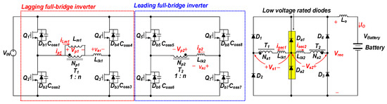
Figure 1.
Proposed DC-DC converter for high-power electric vehicle battery charger.
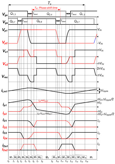
Figure 2.
Key operating waveforms of the proposed converter in steady state.
Each switching period is divided into two half cycles, t0–t8 and t8–t16. Because the operational principles of two half cycles are symmetric, only the first half cycle is described. This half cycle can be subdivided into eight modes, whose operating circuits are shown in Figure 3.
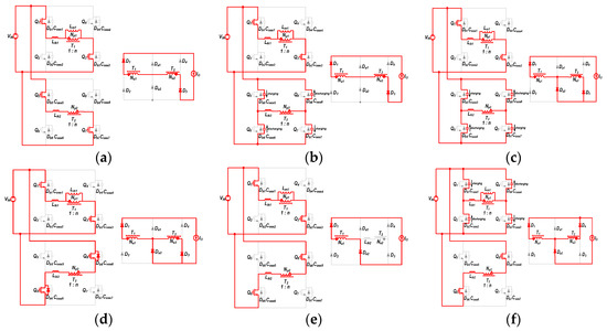
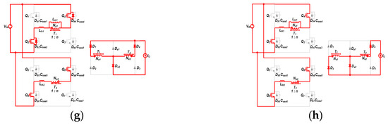
Figure 3.
Operating circuits during the first half cycle: (a) Mode 1; (b) Mode 2; (c) Mode 3; (d) Mode 4; (e) Mode 5; (f) Mode 6; (g) Mode 7; and (h) Mode 8.
For the simplicity of analysis, some assumptions are made as follows:
- (1)
- Two transformers of T1 & T2 have the turns-ratio of n = NS1/NP1 = NS2/NP2 and include the leakage inductors of Llk1 and Llk2, respectively.
- (2)
- The magnetizing inductor (Lm2) of T2 has a sufficient large value to ignore the effect of the magnetizing current.
- (3)
- All the active switches have the same output capacitance of COSS.
- (4)
- The output inductor has a sufficient large value so that it can be seen as a current source.
Mode 1 (t0~t1): Mode 1 begins when the Q5,7 in leading switches and the Q1,3 in lagging switches are in ON-state and the diodes of D1 and D3 are conducting. In this mode, the voltages at the primary side of Vp1(t) and Vp2(t) become positive and negative values of VIN, respectively. The magnetizing current of T1, iLm1(t) starts linearly increasing, but the iLm2(t) is nearly zero due to the very large magnetizing inductance of T2. The voltages at the secondary side of Vs1(t) and Vs2(t) also become positive and negative values of the input voltage with the turns-ratio of n, respectively. The output voltage of rectifier, Vrec(t) becomes 2nVIN due to the sum of Vs1(t) and -Vs2(t). In this mode, the power is transferred from the input port to the output port via T1, T2, D1, and D3 and the primary currents of inverter stage can be expressed as follows:
Mode 2 (t1~t2): Mode 2 begins when the Q5,7 are turned off at t1. Then, with the energy stored in the output inductor LO, the voltages across COSS5 and COSS7 are charged linearly and the voltages across COSS6 and COSS8 are discharged. Vp2(t) increases from −VIN and Vp1(t) is maintained at VIN. The Vrec(t) falls from 2nVIN to nVIN. The expression of primary currents in this mode is the same as in mode 1.
Mode 3 (t2~t3): When the Vp2(t) becomes zero, mode 3 starts. Then the Vs2(t) is zero and the diode of Da2 begins to be ON. Because Da2 is ON, Vs2(t) is maintained at zero in this mode and a resonance behavior between the output capacitances of all the leading switches and Llk2 occurs in the leading full-bridge inverter. With the resonance, the voltages across COSS5&7 are continuously charged and the voltages across COSS6&8 are discharged. The Vp2(t) increases from zero to VIN, and Vp1(t) is maintained at VIN.
Mode 4 (t3~t4): The Vp2(t) becomes VIN in mode 3 and then mode 4 starts. The body diodes of Q6,8, Db6 and Db8, start to conduct and Q6,8 are turned on with ZVS. In mode 4, Vs2(t) is continuously zero, thus the input voltage of VIN applies to the leakage inductor of Llk2. Due to the positive voltage applied to Llk2, Da2 begins to commutate with D3. Vp1(t) and Vrec(t) are maintained at VIN and nVIN, respectively. In this mode, the input power is transferred to the output load through T1, T2, D1, Da2, and D3, and the currents can be analyzed as follows.
Mode 5 (t4~t5): Mode 5 begins when the commutation between D3 and Da2 is completed at t4 and only D1 and Da2 are conducting. In this mode, the ip2(t) is zero, and the input power is transferred to the output load through T1, D1, and Da2.
Mode 6 (t5~t6): Mode 6 starts when Q1,3 are turned off at t5. At the same time, diode D4 starts to conduct and another resonance, which consists of the output capacitances of all the lagging switches and the two leakage inductors of Llk1 and Llk2, occurs in the lagging full-bridge inverter. By the resonance, the voltages across COSS1&3 are discharged, and the voltages across of COSS2&4 are charged. The Vp1(t) decreases from VIN to −VIN and Vrec(t) decreases to zero. The commutation between D1 and D4 is also progressed.
Mode 7 (t6~t7): When the Vp1(t) becomes −VIN in Mode 6, Mode 7 begins. Then the body diodes of Q2,4, Db2 and Db4, start to be ON and Q2,4 is turned on with ZVS. In Mode 7, the Vs1(t) and Vs2(t) are zero, and thus Vrec(t) is also zero. Due to this, the output load is powered from the energy stored in the output inductor LO at t6. Because Vp1(t) = −VIN, Vp2(t) = VIN, and Vs1(t) = Vs2(t) = 0, the voltages across two leakage inductors, Llk1 and Llk2, equal to −VIN and VIN, respectively. Then the ip1(t) and iD1(t) decrease linearly and the ip2(t) and iD4(t) increase linearly as follows.
Mode 8 (t7~t8): Mode 8 begins when the current through D4 reaches to the output current IO and D1 is turned off. Then the Vs1(t) is zero and Vs2(t) becomes nVIN. Thus, the VIN appears on Llk1 and the commutation between D2 and Da2 starts. The Vrec(t) equals to nVIN. The currents in this mode can be represented as follows.
At the end of Mode 8, iD2(t) reaches to IO and the diode of Da2 is turned off naturally. Then, the input power is transferred to the output load through the path of T1, T2, D2, and D4.
3. Circuit Analysis
3.1. DC Analysis
Since the intervals of modes 2, 6, and 8 in Figure 2 are practically very narrow, the output voltage of the rectifier in the proposed converter, Vrec(t) can be simply given as in Figure 4a. Figure 4b shows the counter part in the conventional converter, which is a traditional phase-shift full-bridge (PSFB) converter or a topology consisting of two PSFB converters operated in parallel for larger power processing.
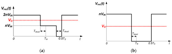
Figure 4.
Simplified rectifier output waveform (a) in the proposed converter and (b) in the conventional converter consisting of two parallel-operated PSFB converters.
In the comparison of the two figures, we can see that the proposed converter do not have freewheeling intervals, where the Vrec(t) is maintained at zero level. Due to this, the proposed converter is able to transfer the input power to the output load continuously, and hence a small inductor can be required for the output filter. And any circulating current is not generated ideally at the primary side. By averaging the Vrec(t) in Figure 4a, the voltage gain of the proposed converter can be acquired as follows.
where TS is a switching period.
From Figure 4b, the voltage gain for the conventional converters is obtained as
The normalized M(D) (supposing n = 1) of the proposed converter is shown in Figure 5 along with the conventional converters. Figure 5 indicates that the proposed converter has much higher voltage gain than the conventional converters. Due to this, the proposed converter can be designed with much smaller turns-ratio (n) than the conventional converter. This contributes to the improvement of the conduction loss in the primary side and the voltage stress on diodes in the secondary side.
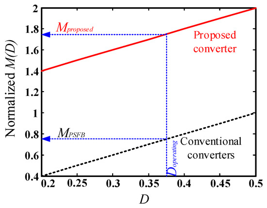
Figure 5.
Normalized DC gain versus duty-cycle.
3.2. Output Inductor
From the voltage and current of the output inductor LO, the LO is can be calculated as
where V is the voltage across LO during the time of ∆T, and Iripple is the current ripple through LO.
Then, for the conventional and proposed converters, the output filter inductor can be obtained as in Equations (8) and (9) using Equations (5)–(7) with Vrec(t)s in Figure 4a,b.
Figure 6 shows the output inductance calculated based on Equations (8) and (9) in function of duty-cycle at the case that VO = 250 V, Iripple = 1A, and fS = 100 kHz. As a result, we can know that the output inductor for the proposed converter is much smaller than it for the conventional converter.
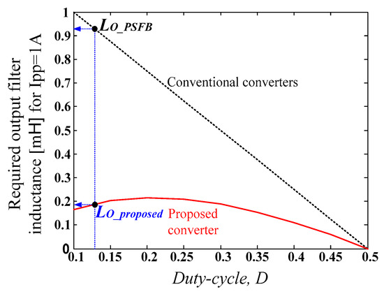
Figure 6.
Required output inductance versus operating duty-cycles.
3.3. Soft Switching Characteristic
As described in the operating modes, the ZVS for the leading switches is formed through two resonant phases. Firstly, by the large energy stored in the output inductor, the drain-to-source voltage of the leading switches is discharged from VIN to 0.5VIN linearly. After that, the voltage is fully discharged by the resonance formed by the energy stored in the leakage inductor Llk2. The ZVS condition for the leading switches can be expressed as follows.
In the view of energy, the Equation (10) can be represented as
As seen in Equation (11), the voltage remaining at the leading switches, which should be removed by the energy stored in Llk2, is only 25% of the original energy. Due to this, the ZVS operation for the leading switches can be acquired easily with the small inductance of Llk2 under wide load variation. If the current through Lm2 is considered to ensure the ZVS, the ZVS equation in Equation (11) can be modified as in Equation (12).
or
where is the current ripple of Lm2. Because the energy that is discharged by is also 25% of the original energy as shown in Equation (12), can be designed with a small value.
The ZVS condition of the lagging switches is obtained as follows.
or
From Equation (13) or (14), it is known that the ZVS of the lagging switches can be easily achieved under wide load variation due to the term of Llk1 + Llk2 and the ripple of iLm1(t), ∆Iripple. Typically, a large leakage inductor increases duty-cycle loss and hence a trade-off between leakage inductor’s values and magnitude of ∆Iripple should be conducted in Equation (14) for optimally designing the proposed converter. In order to extend the ZVS range to no load condition with reasonable leakage inductors’ values, the proposed converter uses the magnetizing inductor of T1, Lm1 (or ∆Iripple) in this paper. Then, someone could think that the conduction loss generated in the lagging full-bridge inverter will increase as in the conventional phase-shift full-bridge converter with a small magnetizing inductance. However, the RMS current in the lagging full-bridge inverter is not increased in spite of the small magnetizing inductance of T1. The average value of the magnetizing current in T1 becomes zero within a half-switching period and thus its contribution to the RMS current is negligible at heavy load conditions. This principle is well explained analytically in [18].
3.4. Operation of the Proposed Converter During Battery Charging
Figure 7 shows the battery charging profile for general battery chargers [19]. At the beginning, the DC-DC converter gradually ramps up charging current with a staircase wave to avoid damaging the battery until each battery cell voltage reaches to the threshold voltage or the battery voltage reaches to point A. This charging sequence is defined as pre-charging mode. After the pre-charging mode, the DC-DC converter is switched to constant-current mode and the battery voltage is linearly charged up to the maximum battery voltage, i.e., 450 V or the point C. If the battery voltage reaches to point C, the DC-DC converter lies finally under constant-voltage mode and the charging current gradually decreases. This mode is stopped when the charging current reaches to the pre-defined termination current as indicated in Figure 7.
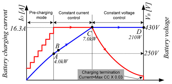
Figure 7.
General battery charging profile [19].
Figure 8 shows the operations, relevant operating waveforms, and equivalent circuits of the proposed converter with the battery charging profile shown in Figure 7. For the pre-charging mode where the processed power is small, the leading full-bridge inverter in the proposed converter is disenabled and only the lagging full-bridge inverter charges up the battery by adjusting the phase-shift time of Tα in between the two legs in the lagging full-bridge inverter indicated in Figure 8a. That is, in this mode, the lagging full-bridge inverter operates like the traditional PSFB converter, and the phase-shift time of Tα decreases as the output voltage or battery voltage increases during the pre-charging mode. When the battery voltage reaches to point A, the Tα becomes zero degree and the gate signal of Q1 (or Q2) is identical with of Q3 (or Q4). At the same time, the leading full-bridge inverter is enabled and the proposed converter starts to work by adjusting the phase-shift time of TΦ between the two inverters as in Figure 2. At point B, most of the power is transferred to the battery through the lagging full-bridge inverter as seen in Figure 8b because the battery voltage is still low or the phase-shift time of TΦ is small. As the charging point moves from A to C, the battery voltage or the charging power increases and TΦ also increases. Then, the power processed by the leading full-bridge inverter gradually increases, and each inverter naturally handles half the total power at the maximum power point, C. These operations make it possible for the proposed converter to achieve higher efficiency during the whole battery charging process.
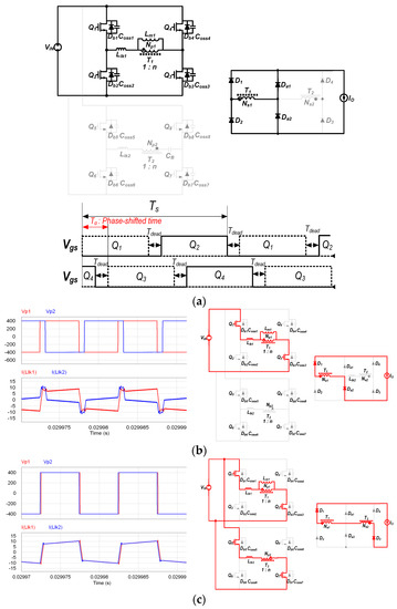
Figure 8.
Operations of the proposed converter with the battery charging profile in Figure 7. (a) In the pre-charging mode; (b) At the point B; and (c) At the point C.
3.5. Voltage Stress
Figure 9 shows the equivalent circuits of the rectifier in the proposed converter during two powering modes. From the figure, the diodes’ voltage stress can be derived as in Table 1. The voltage stress of the two conventional converters is also described in the table, where n is the turns-ratio of the proposed converter and nc1 and nc2 mean the turns-ratios of two conventional converters, respectively. For a quantitative analysis, it is assumed that the input voltage is 400 V, and all the converters operate with the charging profile in Figure 7. Then, each turns-ratio for transformers can be calculated using Equations (10) and (11). However, due to practical factors such as dead-times between driving signals and the duty-cycle loss caused by leakage inductors, the calculated turns-ratios should be lightly increased in practice. Considering this, the turns-ratios are determined as n = 0.61, nc1 = 1.4, and nc2 = 1.22, respectively. Accordingly, it is noted that the proposed converter needs four high-voltage-rated diodes and two low-voltage-rated diodes. On the other hand, both the conventional converters need only high-voltage-rated diodes. Considering that lower-voltage-rated diodes feature many benefits such as much lower voltage drop and better reverse-recovery, the use of two low-voltage-rated diodes for the center-leg in the proposed converter contribute to the reduction of the power loss compared to the two conventional converters, thus enhancing the conversion efficiency.
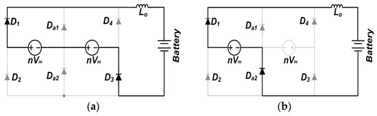
Figure 9.
Equivalent circuits of rectifier stage in the proposed converter during powering modes. (a) Powering operation during Mode 1; (b) Powering operation during Mode 5.

Table 1.
Voltage stress of diodes in the rectifier.
3.6. Loss Comparison and Component Counts
A loss comparison between the proposed converter and conventional converters is carried out at point B, C, and D indicated in Figure 7. Firstly, as indicated in Figure 10, the primary-conduction loss of the proposed converter is much lower than that of the conventional converters. This is because in the proposed converter, the lagging full-bridge inverter processes most of the power at point B and the power at maximum power point C is processed in parallel by both inverters. The smaller turn-ratio also contributes to the reduction of the primary-conduction loss. The primary-switching loss of the proposed converter becomes advantageous as the output power decreases. This is due to the wide ZVS load range. Compared with the conventional converters, the secondary-conduction loss of the proposed converter is also improved due to the deployment of two low-voltage-rated diodes for Da1 and Da2. Figure 10d shows the sum of primary-conduction loss, primary-switching loss, and secondary-conduction loss. Because of the improvements of power loss as shown in Figure 10d, it is possible that the proposed converter achieves higher conversion efficiency compared to the conventional converters during whole battery charging process.
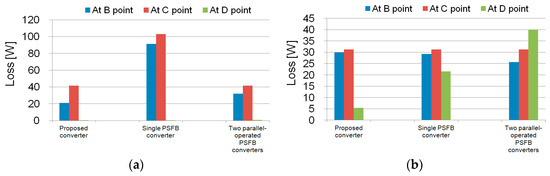
Figure 10.
Loss comparison calculated at 6.6-kW design. (a) Primary conduction loss; (b) Primary switching loss; (c) Secondary conduction loss; (d) Total loss.
Table 2 shows component count. Although the proposed converter handles the high power of over 7-kW, the number of the component in the proposed converter is less than it of the two parallel-operated PSFB converters.
Table 2.
Component count.
In summary, considering the power loss in Figure 10 and the number of components, it can be said that the proposed converter is more suitable than the conventional converters for battery charger applications with the power-capacity of over 7-kW.
4. Experimental Results
In order to confirm the feasibility of the proposed converter, a prototype with the power capacity of 7-kW was built with the following specifications:
- VIN = 400 V, VO = 250–430 V, IO(max) = 16.3 A
- Switching frequency: fS = 100 kHz
Table 3 shows the components used in the prototype converter and the prototype converter is shown in Figure 11.
Table 3.
Component lists.
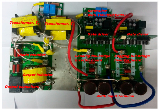
Figure 11.
Prototype of the proposed converter developed at 7-kW.
Figure 12 and Figure 13 show the key operating waveforms when the operating point of the proposed converter is moving from point B to C, which is indicated in Figure 7. As shown in the figures, all the measured waveforms are well following the theoretical waveforms described in Figure 2 and Figure 8. Moreover, it is confirmed from the experimental waveforms that the proposed converter has no circulating current on the primary side during battery charging. We can also see that from the rectifier diodes’ voltage waveforms in Figure 14, the diodes in the center leg of the proposed converter have much lower voltage stress compared to the outer leg diodes. Consequently, the proposed converter can use much better diodes with low voltage rating in the center leg, and the power is transferred using the two low-voltage rated diodes with smaller on-state voltage when the proposed converter moves from point B to C. Due to this operation, the conduction loss in the rectifier stage can be lower than it in the conventional converters.
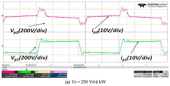
Figure 12.
Vp1, ip1, Vp2, and ip2 when the proposed converter is moving from point B to C.
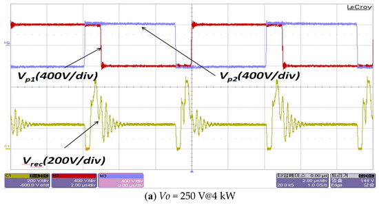
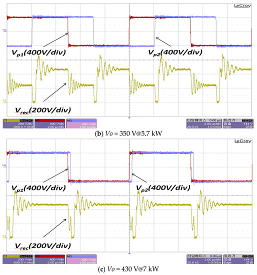
Figure 13.
Vrec when the proposed converter is moving from point B to C.
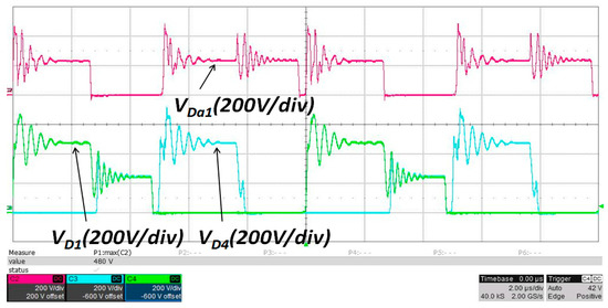
Figure 14.
Diode voltage stress when Vo = 350 V@5.7 kW in the CC charging.
Figure 15 and Figure 16 show the ZVS waveforms during the constant-current (CC) charging mode. During the overall charging mode in Figure 7, all the switches in the proposed converter are turned on after the drain-to-source voltage decays zero as in the waveforms.
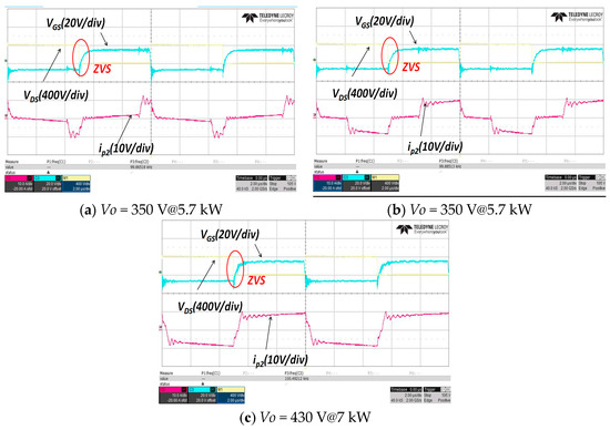
Figure 15.
ZVS waveforms in the lagging full-bridge inverter side during the CC charging.
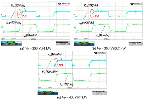
Figure 16.
ZVS waveforms in the leading full-bridge inverter side during the CC charging.
Figure 17 shows the measured efficiencies. As seen in Figure 17, the proposed converter has the maximum of 96.7% at the full load or the point C in Figure 7, and the high efficiency is maintained during the battery charging. This is due to ZVS operation under all operating conditions, the design without the effect of duty-loss, much reduced circulating current, and the two lower-voltage-rated diodes in the rectifier.
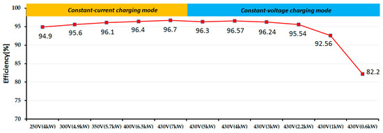
Figure 17.
Measured efficiency during battery charging
In the Figure 18, the output inductors in the conventional PSFB and proposed converters, which are designed at 7-kW, are compared. As analyzed in the Section 3, the proposed converter uses a much smaller inductor.
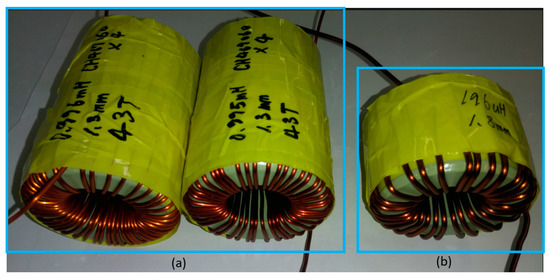
Figure 18.
Output inductors for the charging current ripple of 1A at fs = 100 kHz and Vo = 250 V: (a) the output inductors for the conventional PSFB converters and (b) the output inductor for the proposed converter.
5. Conclusions
This paper proposes a DC-DC converter that can be applied for battery chargers with the power-capacity over 7-kW for EVs. Its advantages are summarized as follows:
- (1)
- Considerable reduction of both primary- and secondary-conduction losses due to the parallel connection in the primary side and the use of two lower-voltage-rated diodes in the secondary side
- (2)
- Additional reduction of primary-conduction loss by no circulating current
- (3)
- Much better turn-ratio by less duty-loss compared to the conventional PSFB converter
- (4)
- Wider ZVS range in all the switches
- (5)
- Much smaller output inductor size
- (6)
- Easy-to-increase power handing capability
The theoretical analysis of the proposed converter was presented in detail, and its feasibility was verified through the experiment with a 7-kW prototype converter. The experimental results show that the proposed converter can be applied for EV battery charger applications with higher power-capacity.
Acknowledgments
This research was supported by Basic Science Research Program through the National Research Foundation of Korea (NRF) funded by the Ministry of Science, ICT & Future Planning (2015R1C1A1A01051992).
Author Contributions
Il-Oun Lee defined the overall outline of the study and performed the numerical analysis, analyzed the data and drafted the paper. Il-Oun Lee designed and performed the experiments; Jun-Young Lee performed the analysis and experiments and finalized the paper.
Conflicts of Interest
The authors declare no conflict of interest.
References
- Rajashekara, K. Present Status and Future Trends in Electric Vehicle Propulsion Technologies. IEEE J. Emerg. Sel. Top. Power Electron. 2013, 1, 3–10. [Google Scholar] [CrossRef]
- Musavi, F.; Edington, M.; Eberle, W.; Dunford, W.G. Evaluation and Efficiency Comparison of Front End AC-DC Plug-in Hybrid Charger Topologies. IEEE Trans. Smart Grid. 2012, 3, 413–421. [Google Scholar] [CrossRef]
- Yang, G.; Draugedalen, E.; Sorsdahl, T.; Liu, H.; Lindseth, R. Design of high efficiency high power density 10.5 kW three phase on-board-charger for electric/hybrid vehicles. In Proceedings of the International Exhibition and Conference for Power Electronics, Intelligent Motion, Renewable Energy and Energy Management, Nuremberg, Germany, 10–12 May 2016; pp. 113–119. [Google Scholar]
- Haghbin, S. Design Considerations of a 50 kW Compact Fast Charger Stations Using Nanocrystalline Magnetic Materials and SiC Midules. In Proceedings of the 11th International Conference on Ecological Vehicles and Renewable Energies (EVER), Monte Carlo, Monaco, 6–8 April 2016. [Google Scholar]
- Kim, J.; Lee, I.; Moon, G. Analysis and Design of a Hybrid-Type Converter for Optimal Conversion Efficiency in Electric Vehicle Chargers. IEEE Trans. Ind. Electron. 2016, 64, 2789–2800. [Google Scholar] [CrossRef]
- Lee, I. Hybrid DC-DC Converter with Phase-Shfit or Frequency Modulation for NEV Battery Charger. IEEE Trans. Ind. Electron. 2016, 63, 884–893. [Google Scholar] [CrossRef]
- Kim, J.; Lee, I.; Moon, G. Integrated Dual Full-Bridge Converter with Current-Doubler Rectifier for EV Charger. IEEE Trans. Power Electron. 2016, 31, 942–951. [Google Scholar] [CrossRef]
- Yu, W.; Lai, J.; Lai, W.; Wan, H. Hybrid Resonant and PWM Converter with High Efficiency and Full Soft-Switching Range. IEEE Trans. Power Electron. 2012, 27, 4925–4933. [Google Scholar] [CrossRef]
- Cho, Y.; Lai, J.S. Digital Plug-In Repetitive Controller for Single-Phase Bridgeless PFC Converters. IEEE Trans. Power Electron. 2013, 28, 165–175. [Google Scholar]
- Musavi, F.; Eberle, W.; Dunford, W.G. A High-performance Single-Phase Bridgeless Interleaved PFC Converter for Plug-in Hybrid Electric Vehicle Battery Chargers. IEEE Trans. Ind. Appl. 2011, 47, 1833–1843. [Google Scholar] [CrossRef]
- Yilmaz, M.; Krein, P.T. Review of Battery Charger Topologies, Charging Power Levels, and Infrastructure for Plug-In Electric and Hybrid Vehicles. IEEE Trans. Power Electron. 2013, 28, 2151–2169. [Google Scholar] [CrossRef]
- Garcia, O.; Zurnel, P.; de Castro, A.; Cobos, A. Automotive dc-dc bidirectional converter made with many interleaved buck stages. IEEE Trans. Power Electron. 2006, 21, 578–586. [Google Scholar] [CrossRef]
- Lee, J. An EL Capacitorless EV On-Board Charger Using Harmonic Modulation Technique. IEEE Trans. Ind. Electron. 2014, 61, 1784–1787. [Google Scholar] [CrossRef]
- Zhang, D.; Wang, F.; Burgos, R.; Boroyevich, D. Total Flux Minimization Control for Integrated Inter-Phase Inductors in Paralleled, Interleaved Three-Phase Two-Level Voltage-Source Converters with Discontinuous Space-Vector Modulation. IEEE Trans. Power Electron. 2012, 27, 1679–1688. [Google Scholar] [CrossRef]
- Luo, S.; Ye, Z.; Lin, R.; Lee, F.C. A Classification and Evaluation of Paralleling Methods for Power Supply Modules. In Proceedings of the 30th Annual IEEE Power Electronics Specialists Conference, Charleston, SC, USA, 1 July 1999; pp. 901–908. [Google Scholar]
- Pahlevaninezhad, M.; Das, P.; Drobnik, J.; Jain, P.; Bakhshai, A. A ZVS Interleaved Boost AC/DC Converter Used in Plug-in Electric Vehicles. IEEE Trans. Power Electron. 2012, 27, 3513–3529. [Google Scholar] [CrossRef]
- Qahouq, J.A.A.; Huang, L.; Huard, D. Efficiency-Based Auto-Tuning of Current Sensing and Sharing Loops in Multiphase Converters. IEEE Trans. Power Electron. 2008, 23, 1009–1013. [Google Scholar] [CrossRef]
- Lee, I.; Moon, G.W. Phase-Shifted PWM Converter with a Wide ZVS Range and Reduced Circulating Current. IEEE Trans. Power Electron. 2013, 28, 908–919. [Google Scholar] [CrossRef]
- Kang, T.; Kim, C.; Suh, Y.; Park, H.; Kang, B.; Kim, D. A Design and Control of Bi-directional Non-isolated DC-DC Converter for Rapid Electric Vehicle Charging System. In Proceedings of the 27th Annual IEEE Applied Power Electronics Conference and Exposition, Orlando, FL, USA, 5–9 February 2012; pp. 14–21. [Google Scholar]
© 2017 by the authors. Licensee MDPI, Basel, Switzerland. This article is an open access article distributed under the terms and conditions of the Creative Commons Attribution (CC BY) license (http://creativecommons.org/licenses/by/4.0/).