1. Introduction
DC-DC converters have been widely used or proposed for different applications, recently for grid-tied renewable power conversion systems [
1,
2,
3,
4]. For the most part their applications are projected for photovoltaic (PV) systems [
5,
6,
7,
8]. However, they can be adopted for use with any renewable energy sources that have a DC-conversion stage. Since the power transmission from distant or offshore renewables is efficient in medium or high voltage, conventional converter topologies are replaced by their multilevel counterparts. This power transfer is often fulfilled by multiple power conversion stages. The DC-DC converters regulate the DC-link voltage in common DC-link systems. The normal boost operation used for supporting neutral point clamped (NPC) inverters in grid-connected photovoltaic systems can be replaced with multilevel DC-DC converters for improving the overall performance of the system. In addition, they play a key role in resolving the drawbacks of certain multilevel inverter topologies. For example, many topologies are subjected to circulating current or capacitor voltage imbalance problems. These issues can either be solved by modulation strategies or by additional hardware circuits. Several DC-DC converter configurations are proposed for voltage balancing [
9,
10,
11,
12,
13,
14,
15]. A three-level boost converter with a new PDC strategy is proposed for the DC-link voltage regulation and neutral point voltage balancing for three-level neutral point clamped (NPC) inverter; see [
13,
14]. In [
14], the improvement in converter cross-regulation capability with PDC for TLBC is compared to the conventional three-level boost control and enhancements are listed clearly.
In many renewable energy conversion scenarios, the generated voltage output can become higher or lower than the rated DC-link voltage of the power converter system. In such cases, it is vital to have both buck and boost capabilities for the DC-DC converter to maximize the system utilization. In such situations, the conventional boost and the TLBC become inadequate. Considering the above aspects, the current work proposes DIDO-type TLBBC with a PDC strategy for enhanced power conversion and balancing performance.
Section 2 discusses the basic TLBBC circuit with its four distinct operating modes and characteristics. Ten different operational cases of TLBBC and their contributions for voltage cross regulation, along with the equations for neutral voltage calculation in each case is presented in
Section 3. Validation of analytical results using simulations are also presented in this section. A brief discussion of closed-loop controller design is given in
Section 4, while the simulation results are presented in
Section 5. Cross-regulation comparisons of TLBC and TLBBC are presented with 3D plots in
Section 6. In
Section 7, experimental setup and test results are described along with a comparison of neutral voltage from analytical, simulation and experimental methods. Final conclusions from the work are presented in
Section 8.
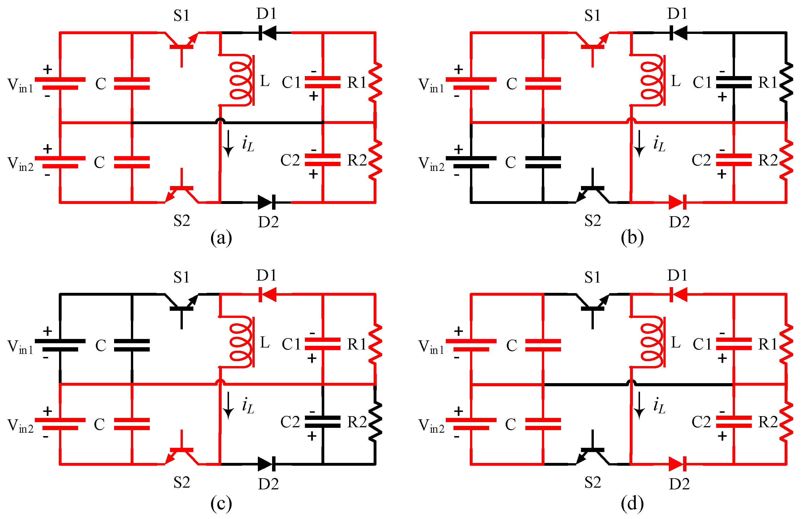
2. Three-Level Buck-Boost Converter—Modes of Operation
This section discusses about the basic TLBBC circuit with the four operating modes [
16], as shown in
Figure 1. Depending on the position of the switches
and
, there are four modes of operation for the TLBBC: mode1, mode2, mode3, and mode4. Each mode of operation with corresponding voltage and current equations are presented below, where
p denotes the time derivative
.
Figure 1 shows the current paths during each mode in red.
2.1. Mode1: S1 and S2 ON
In Mode1, both S1 and S2 are ON. The inductor
L is charged by the sources,
Vin1 and
Vin2 and hence the current via inductor,
, increases linearly. The capacitors C1 and C2 discharge through load resistors R1 and R2, as shown in
Figure 1a. The steady state voltage and current Equations are given by Equation (1):
where
and
are the voltages across the capacitors C1 and C2, respectively, and R1 and R2 are the load resistors.
2.2. Mode2: S1 ON and S2 OFF
In Mode2, S1 remains ON whereas S2 is turned OFF, as shown in
Figure 1b. The inductor
L is charged by the source,
Vin1 and current flows from input via inductor
L to resistor R2. The capacitor C2 is charged whereas C1 discharges through resistor R1. The voltage across C1 decreases and that of C2 increases, and thereby creates an imbalance at the output. The steady state Equations are given by Equation (2):
2.3. Mode3: S1 OFF and S2 ON
This mode is quite like the previous mode. The current flows from input
Vin2 via inductor
L to resistor R1. The capacitor C1 is charged while C2 discharges through resistor R2. In this mode, the voltage across C1 increases and C2 decreases, resulting in an imbalance. The flow of current is shown in
Figure 1c. The steady state Equations are given by Equation (3):
2.4. Mode4: S1 and S2 OFF
If both S1 and S2 are OFF, then there is no direct energy transfer from source to load. The inductor
L discharges to the load and, hence, the current
decreases linearly. There will not be any unbalanced voltage at the output. The flow of current is shown in
Figure 1d. The state space Equations are given by Equation (4):
form the modes of operation listed above; it is clear that the TLBBC has different characteristics during each mode. The modes 1 and 4 are primarily responsible for the conventional buck-boost type converter operation, while the modes 2 and 3 are capable for the cross-regulation/voltage balancing.
3. Operational Cases, Open-Loop Control Equations and Cross-Regulation Verification
From the detailed analysis of TLBBC operation using different combination, sequencing and timing of TLBBC operating modes, it is found that the converter can go through 10 different operational cases during its entire range of operation as shown in
Table 1. The analysis is based on the assumption that the converter stays in continuous current mode (CCM) during all the cases of operation. These cases can be used for the mathematical modeling of the DC-link voltage and thereby enable the design of the controller. The inductor ripple current is different in each case. Therefore, the conventional state space averaging technique cannot be applied to all the cases. The inductor ripple current averaging technique with state space averaging method is the best suited [
14,
17]. Using this method, the voltage difference ∆
V for each case is modeled.
Table 1 also gives the expression of ∆
V for all 10 cases of operation of the TLBBC.
It should be noted that the case I and case IV with only two modes of operation in each case will not be able to contribute for cross regulation purposes. However, they can be used for the normal buck-boost operation. In particular, case I, which includes mode1 and mode4, is similar to the conventional buck-boost converter operation and can be used for the total voltage control of the TLBBC output by using a duty ratio control similar to the conventional buck-boost regulation. Case IV is, however, not present in the conventional converter, and it charges and discharges the two capacitors equally during alternative switching modes. This causes the average voltage change in a cycle to become zero and cannot contribute to cross-regulation application. All the other cases, except case I and case IV, can contribute to cross-regulation purposes, and the intelligent use of these cases during closed loop control of TLBBC can enhance the cross-regulation capabilities of the TLBBC while optimizing the performance and stability.
Where
d is the duty ratio of the switches,
λ is the pulse delay ratio (delay between switch gate pulses/switching period) and
is a function of input and output voltages, which is defined in Equation (5):
The voltage imbalance, ∆
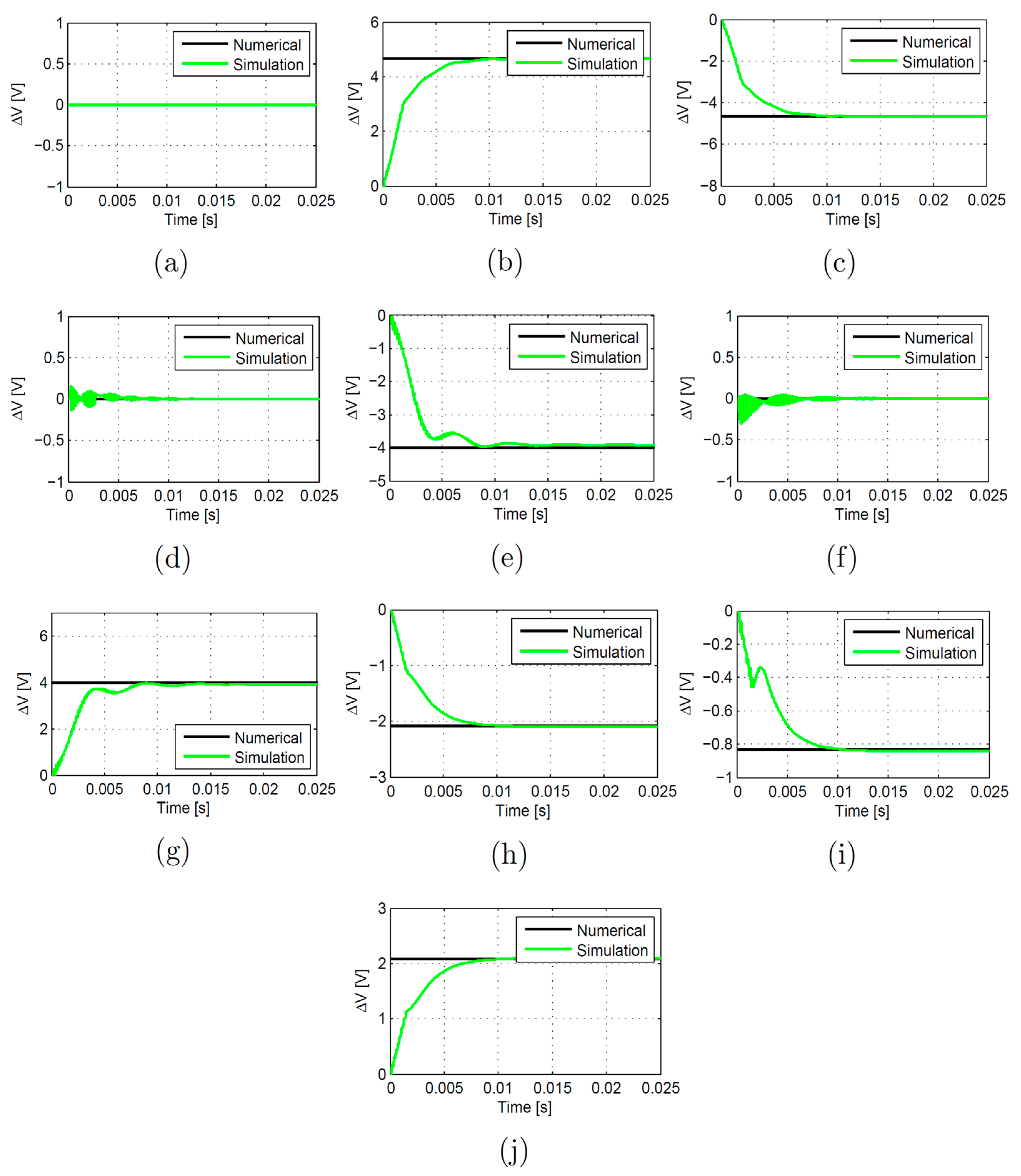
V, obtained mathematically, can be compared with the value given by the simulation for each case.
Figure 2 shows the value of ∆
V obtained from calculation and in open-loop simulation. It is shown that both the results are almost equal. The simulation parameters used are given in
Table 2.
4. Closed-Loop Controller Modelling
The DC-link voltage regulation is carried out by using the buck-boost capability of the system very similar to the conventional buck-boost converter control. The steady state output voltage,
V0, of the buck-boost converter can be calculated using the input voltage,
Vin, and the duty ratio,
d, as shown in Equation (6). Depending on the value of
d, the converter either increases or decreases the voltage given to the input.
To get the desired output voltage for a varying source voltage, the duty ratio must be controlled. The proportional integral (PI) controller computes the value of duty ratio,
d, required for achieving the desired output voltage. The Equation of the controller for voltage regulation is given by (7):
where
and
are the proportional and integral controller parameters, and the error,
;
, is the desired DC-link voltage, and
is the actual output voltage.
In TLBBC, the two switches are operated with the same duty ratio. The phase between the control signals of the switches is varied to minimize the neutral point voltage ideally to zero. The gate signal of one switch is kept constant, while the phase of the other signal is varied. The voltage deference between the output capacitors, ∆
V, is sensed and is used in a PI controller to calculate a pulse delay ratio, as shown in Equation (8). This delay is given to one of the switch pulse signal to move it either forward or backward with respect to the other pulse signal in order to compensate for the neutral point voltage.
where
and
are the PI controller parameters,
.
Applying perturbations to the state variables, the expression of the neutral point voltage for AC analysis can be formulated. Considering case 2 for illustration, the system transfer function is given as shown in Equation (9):
where
T is the switching period. Since a PI controller is used, the closed-loop transfer function
Gc is given by Equation (10):
To find the value of and , equate the characteristic equation of (10) to zero. The controller can be tuned using these values. For example, in case II, the values of and are 0.1596 and 33.9605, respectively. It is observed that the same value of and satisfies other cases of the operation of the TLBBC as well. The simulation results show the maximum values of ∆V that the system can achieve with the feasible values of d and λ.
5. Simulation Results
Depending on the switching states, the TLBBC can be operated either as a normal buck-boost converter or as a cross-voltage compensator. The operating regions of the converter are determined by the duty ratio of the switch-gate signals and the pulse delay between them. Duty ratio is used for conventional buck-boost action and pulse delay gives the voltage cross regulation. To analyze these operations, the TLBBC circuit is simulated for a switching frequency of 5 kHz in MATLAB/Simulink under ideal conditions.
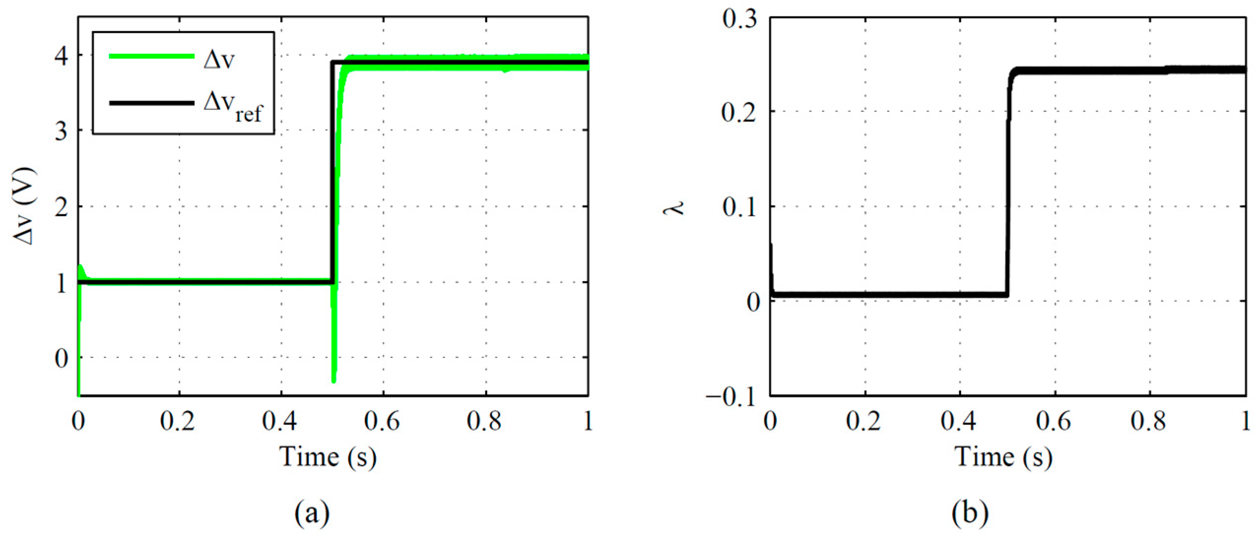
Table 2 shows the specifications used for the simulations. For a step variation of the reference voltage ∆
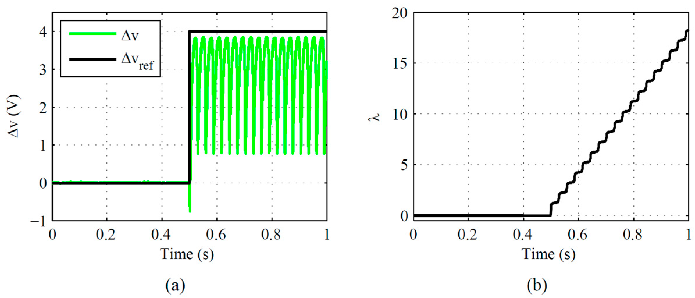
V from 1 V to 3.9 V, the system follows the input and gives the maximum response. The corresponding pulse delay ratio is just below 0.25.
Figure 3 shows the corresponding waveforms. The settling time is 0.03 s. For values greater than or equal to 4 V, the converter saturates and the system starts oscillating, as shown in
Figure 4a. The corresponding pulse delay variation is shown in
Figure 4b.
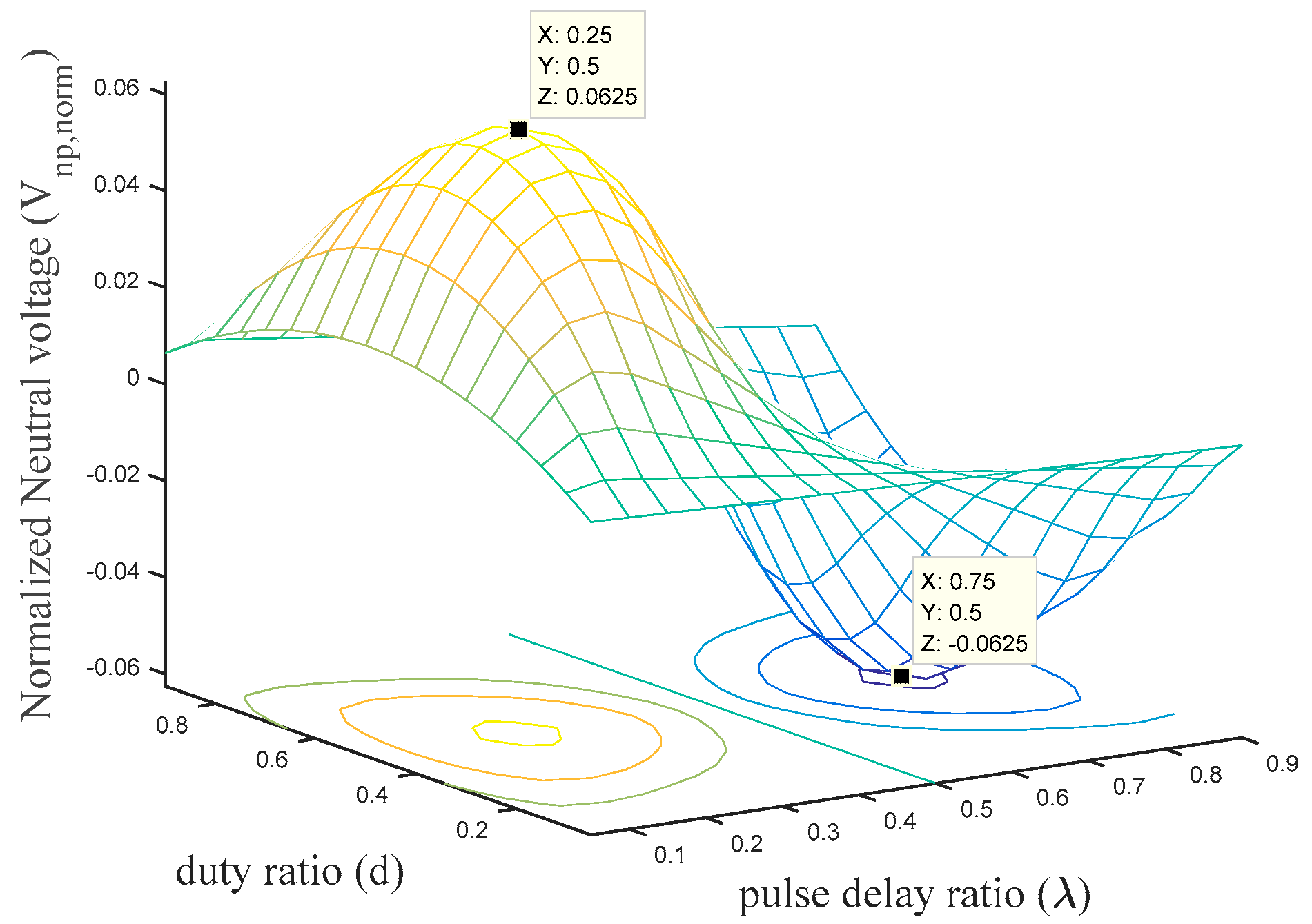
6. Comparison with Three-Level Boost Converter
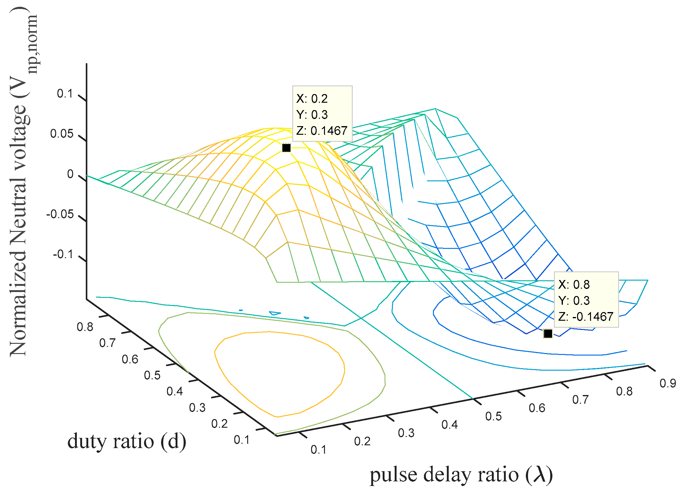
The cross-regulation capabilities of a TLBBC and a three-level boost converter (TLBC) are compared under the PDC control method. The maximum cross-regulation voltages are calculated for all the 10 cases. The corresponding 3D-plots are shown below. For TLBC, the maximum normalized cross-regulation voltage is ±0.0625; see
Figure 5. For TLBBC, this value is ±0.1467; see
Figure 6. It shows that the TL buck-boost converter has better cross-regulation capability compared to the TL boost converter under same cross-voltage regulation method.
The cross-regulation voltage values in the figures below indicate the theoretical maximum for each duty ratio and pulse delay ratio. However, in practical scenarios, these values can be lower than that calculated here. The peracetic drops, the component lead impedances and losses in the switches and diodes restrict the converter to achieve these peak values. The parameters used for this simulation is also the same as the parameters used for the previous simulations and listed in
Table 2.
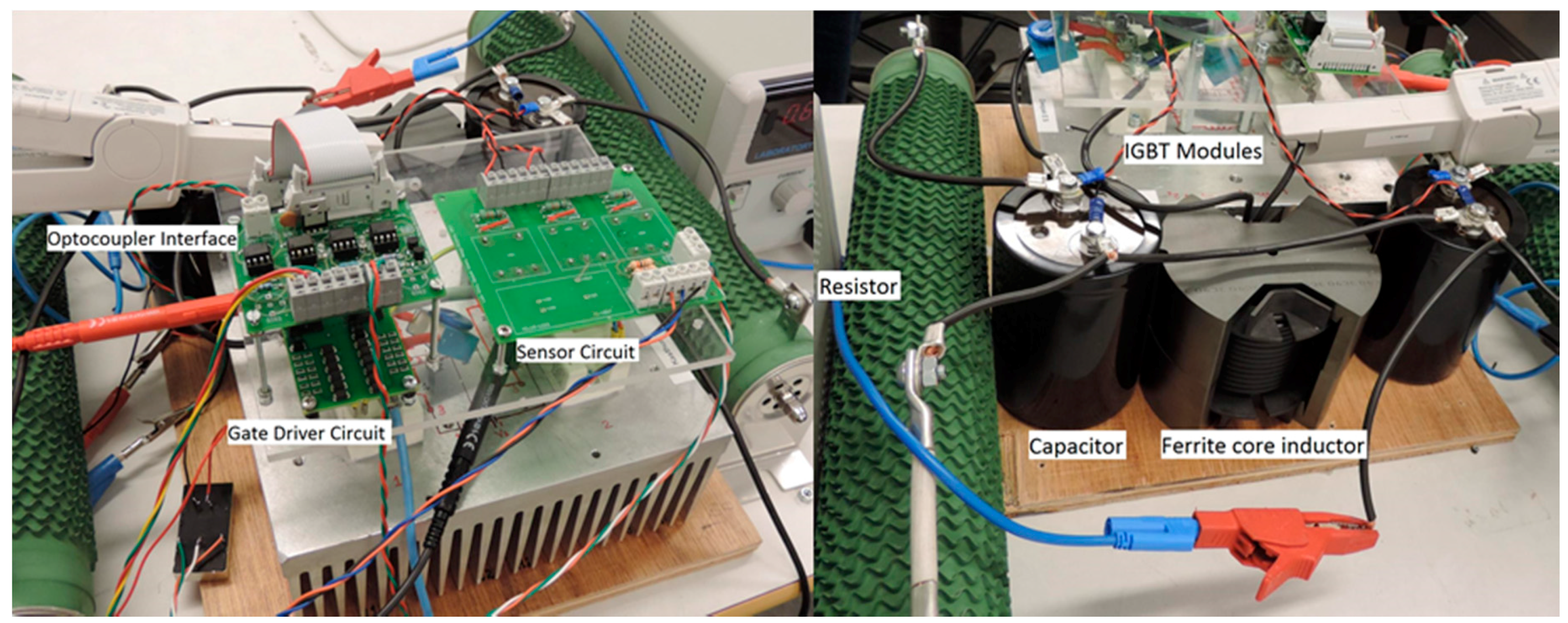
7. Experimental Results
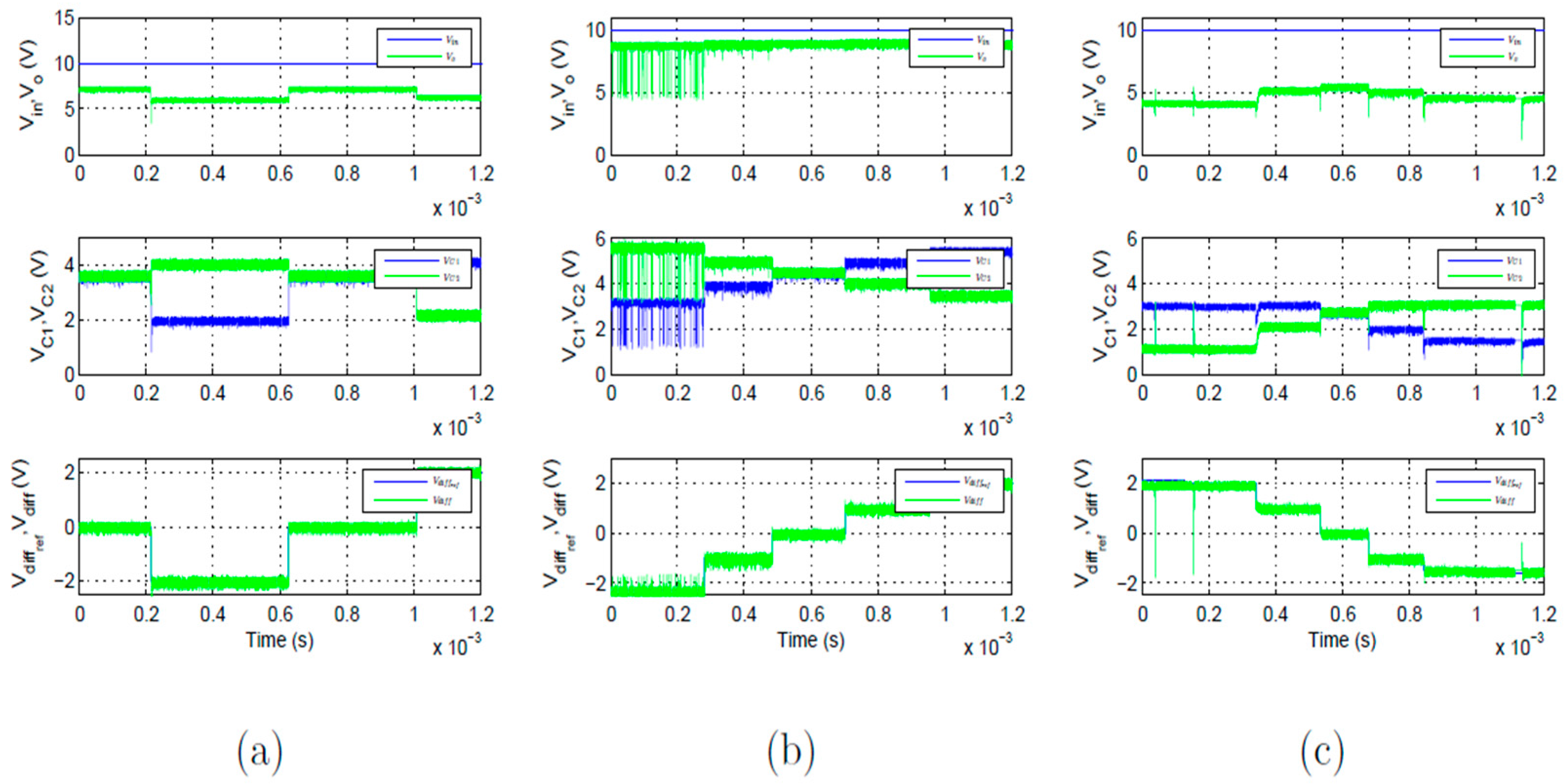
The converter design mainly consists of the selection of IGBT modules. The IGBT module BSM50GB120DN2 from Infineon is used as the switches. It is a high-power module and can handle high voltages of up to 1200 V. The free-wheeling diodes in the module are used as the diodes of the converter circuit. An air-gapped ferrite core with copper winding is used as inductor. Snubbers and varistors are also included to protect the circuit from high voltages and transient peaks. The experimental setup of the converter hardware is shown in
Figure 7. The input voltages, the output capacitor voltages and the cross-regulation performance of the converter results from the experiment for boost and buck mode is shown in
Figure 8.
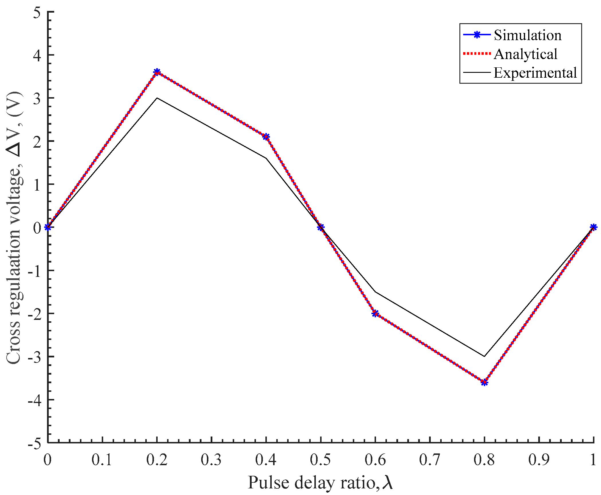
In
Figure 9, the cross-regulation voltages in calculation, simulation and experiment are compared. The mathematical analysis and simulation results give very similar results while the experimental results are slightly lower. This is due to the losses present in the converter hardware which are not present in the analytical and simulated results assuming ideal conditions.
8. Conclusions
The three-level buck-boost converter is analyzed to find the amount of cross-regulation it can provide. This analysis is significant for various renewable energy grid integration scenarios where the three-level NPC inverter is used for grid coupling. Varying input from renewable sources imposes high-input cross-regulation requirements for the NPC. A new type of PDC cross-regulation method is proposed to compensate for the imbalance produced at the NPC input. Different operating modes of the TLBBC circuit are analyzed and 10 cases of operation are found, which can be used to control efficiently the maximum possible oprating range of the converter. The expression for the voltage imbalance for each case is formulated using ripple current averaging method. Moreover, the simulation in Matlab/simulink validates the voltage imbalance created in each of these 10 cases. A closed-loop controller using PI controllers is designed based on the operatinal case equations in order to achieve the desired voltage compensation. When PDC and convensional duty ratio controls are combined, the converter gives full performance by providing both output voltage control, as well as cross regulation. The cross-regulation capability of the TLBBC converter is compared to the TLBC converter to show its superiority in cross regulation. The simulation results are verified using experimental results. The results shows that the TLBBC has a better cross-regulation capability, which can be really useful to support three-level NPC based renewable grid integration. In this study, the input voltages are considered as equal. However, it would be of interest to see the converter feasibility with unequal input voltage. This is considered as an area future study.


