Article

ITO-Free Transparent Organic Solar Cell with Distributed Bragg Reflector for Solar Harvesting Windows

1
Department of Electrical and Computer Engineering, University of Wisconsin-Madison, Madison, WI 53706, USA
2
Department of Chemistry, University of Massachusetts Amherst, Amherst, MA 01003, USA
3
Department of Chemistry, University of Wisconsin-Madison, Madison, WI 53706, USA
*
Author to whom correspondence should be addressed.
Energies 2017, 10(5), 707; https://doi.org/10.3390/en10050707
Submission received: 30 March 2017 / Revised: 8 May 2017 / Accepted: 11 May 2017 / Published: 17 May 2017
(This article belongs to the Special Issue Solar Energy Application in Buildings)

Abstract

:
We demonstrated an indium tin oxide (ITO)-free, highly transparent organic solar cell with the potential to be integrated into window panes for energy harvesting purposes. A transparent, conductive ZnO/Ag/ZnO multilayer electrode and a Ag:Ca thin film electrode were used in this transparent device as the bottom and top electrode, respectively. To further improve the transmittance of the solar cell, the thickness of the top ZnO layer was investigated both experimentally and with simulations. An average visible transmittance of >60% was reached, with a maximum transmittance of 73% at 556 nm. Both top and bottom illumination of the solar cell generated comparable power conversion efficiencies, which indicates the wide application of this solar cell structure. In addition, we fabricated distributed Bragg reflector mirrors with sputtered SiO2 and TiO2, which efficiently increased the power conversion efficiency over 20% for the solar cells on glass and poly(ethylene terephthalate) (PET) substrates.

1. Introduction

Organic solar cells (OPV) persist in drawing researchers’ attention due to their low-cost and easy-processing requirements. Since Tang published the first organic heterojunction solar cell in 1986, the energy harvesting efficiency of OPVs has greatly increased due to optimized electronic device structures and by incorporating novel absorber materials [1,2,3,4]. Besides the pursuit of high power efficiency, OPVs have also been investigated for various potential applications [5,6]. Transparent OPVs, i.e., devices that seem transparent to the human eye due to high transmissivity between 400 nm–700 nm, can be integrated into window panes or screens of consumer electronic devices [7]. The key to constructing a transparent solar cell is to find a suitable transparent electrode and absorbers with an absorbance peak beyond the visible region [8].
Transparent conductors, such as metal thin films, doped metal oxides, metal nanowires, conducting polymers, and graphene have been used as electrodes in transparent solar cells [9,10,11,12]. However, these electrodes suffer from various problems, including low transparency and/or high roughness, that hinder the creation of efficient transparent OPVs that can be easily integrated into complicated fabrication process flows and larger circuits. Furthermore, in some cases, the necessary methods to deposit films of these electrodes often damage, corrode, or destroy underlying organic layers [13,14]. Indium tin oxide (ITO), which is the most commonly used transparent electrode material, has high brittleness and low infrared transmittance that limits its use in many large-scale, high-performance optical applications [15]. Silver and zinc oxide (ZnO) based multilayer transparent electrodes have been well investigated due to their high conductivity and transparency [16]. However, most prior research focused on optimizing and understanding the transmittance of the Ag and ZnO based electrode itself [17,18,19]. There is a lack of reporting about incorporating this kind of electrode into a functioning nanostructured device.
Here, we present a transparent planar heterojunction organic solar cell containing molecular organic donor and acceptor materials, which have peak-absorption in the ultraviolet (UV) and near-infrared (NIR) regions as Figure 1 shows. A trilayered ZnO/Ag/ZnO (ZAZ) transparent electrode is presented as the bottom electrode for this transparent organic solar cell. The optical and electrical properties of the electrode itself, and the electrode with the whole solar cell, are investigated experimentally and with simulations. A second transparent electrode comprised of blended Ca and Ag is used as the top contact of the organic solar cell. This solar cell reached a similar device performance with both top and bottom illumination, a feat that is uncharacteristic of most organic solar cells, which are constructed on transparent substrates with one opaque contact and can only function under bottom illumination [20]. This unique feature will allow this device to be easily incorporated into large solar arrays that are similar in design and layout to existing solar panels, thus providing a simple and effective strategy to create OPV arrays using existing manufacturing methods. In order to further improve the current density of the solar cell, an optimized distributed Bragg reflector (DBR) is used as a transparent NIR mirror with an average transmittance >95%. The transparent solar cell and the DBR deposited on PET substrate have similar device performance as the glass-based solar cells with top illumination, which makes it possible to deposit arrays of this device on flexible substrates.

2. Results

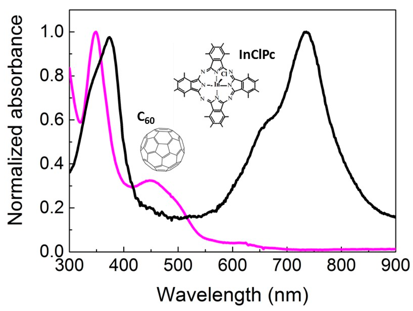
2.1. Donor and Acceptor Layers for the Organic Solar Cell

The ideal photoactive materials for a transparent solar cell should absorb ultraviolet and near-infrared photons while being transparent to visible photons. We define the visible range as the wavelengths from 400 to 700 nm. In this solar cell, we utilize a molecular organic donor, chloroindium(III) phthalocyanine (ClInPc), and a molecular acceptor, C60. Both of these two materials show absorption peaks in the ultraviolet and near-infrared regions. Figure 2 shows the molecular structures and the normalized thin film absorbance of ClInPc and C60. C60 has strong photosensitivity from 350 nm to 500 nm with a peak at 348 nm, consistent with previous reports [21]. ClInPc shows two broad peaks centered at 373 nm and 734 nm, but no absorption band between 400–650 nm [22]. The total spectrum coverage of these two donor and acceptor materials ensures the acceptable visible-region transmittance of a device constructed from these materials. Both of these two materials were deposited by a thermal evaporator with a rate of 0.4 Å/s.

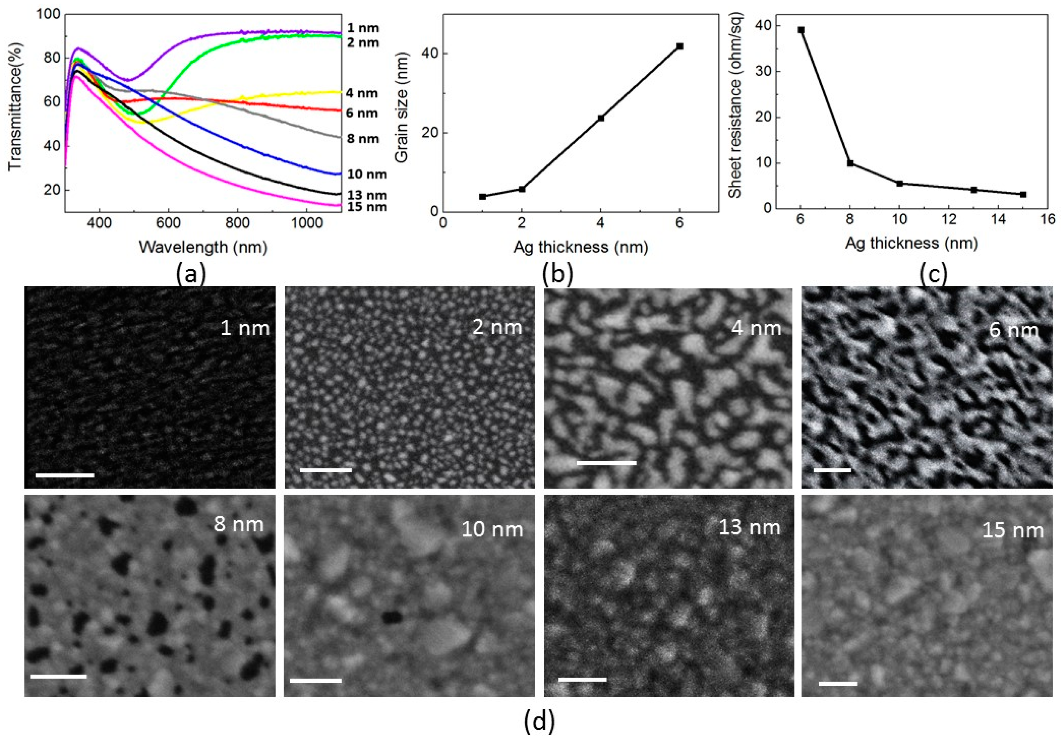
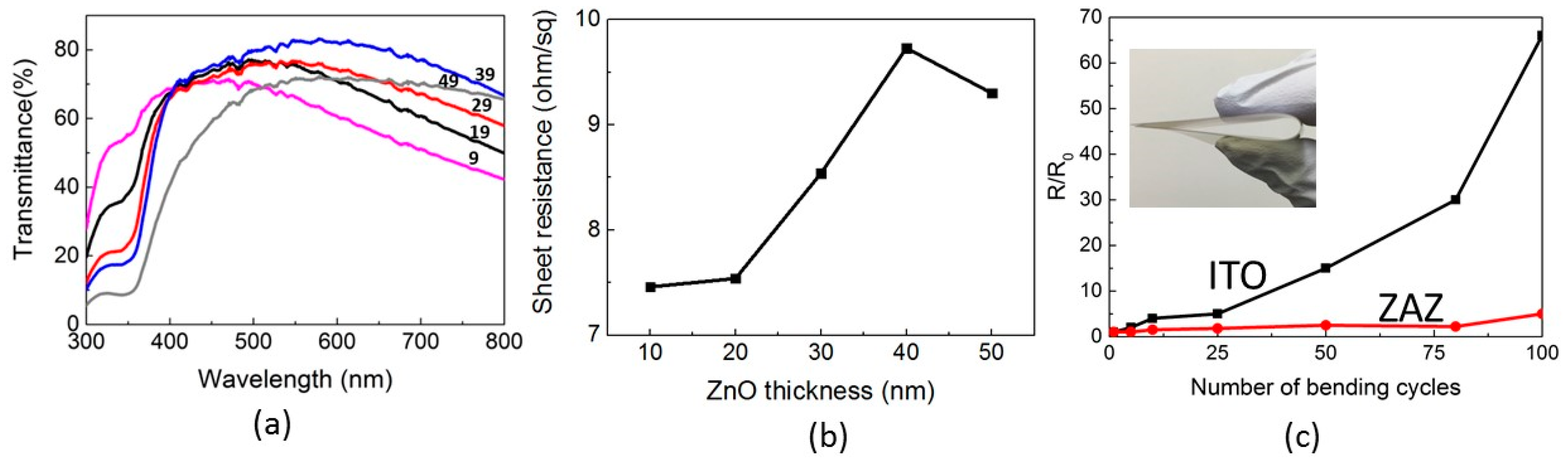
2.2. Transparent Bottom Electrode

Both electrodes of the transparent solar cell are required to have high transmittance and high conductivity. Here we define the electrode that is deposited on top of the organic photoactive layers as the top electrode, and the one that is below the photoactive layers and closest to the substrate as the bottom electrode. Transparent metal oxides with a sandwiched thin metal film, or a dielectric/metal/dielectric (D/M/D) multilayer structure, have been actively investigated for optoelectronic applications [23,24,25,26,27]. The metal oxide layers can efficiently suppress the reflection from the metal and achieve a high transmittance in the visible region. Silver was commonly used as the middle metal layer due to its low sheet resistance [28]. ZnO was chosen as the dielectric material because it is nontoxic, cheap, and abundant in nature [29]. In this work, a ZnO/Ag/ZnO multilayer electrode was used as the bottom electrode.
Figure 3a shows the optical transmittance of Ag thin films formed on glass substrates with various thickness from 1 to 15 nm and a constant sputter rate of 2.5 Å/s. When the sample thickness is less than 8 nm, there is a broad dip in the transmittance spectrum, indicative of the localized surface plasmon resonance of the metal nanoparticles [30]. In this case, Ag most likely diffused locally and formed small isolated islands as nanoparticles during the deposition. The plasmon resonance dip red-shifts and broadens as the Ag thickness increases, due to the increased particle size, as Figure 3b reveals [31]. As the thin film keeps growing, the neighboring particles get closer to each other and coalesce. This coalescence leads to Ag islands formed with irregular shapes and fractal structure growth. When the thickness of the Ag film is greater than 8 nm, multiple isolated islands start to form larger clusters, resulting in a quasi-continuous film [32]. The transmittance decreases past 350 nm, indicating the formation of a continuous metal film. The continuous Ag film greatly improved its electrical performance. When the film thickness was less than 6 nm, the sheet resistance of the film is too large to be measured. When the thickness of the film increased from 6 to 15 nm, the sheet resistance decreased from 39.2 to a useable value of 3.2 ohm/square.
Figure 4a shows the transmittance spectra of the ZAZ electrode as a function of the ZnO layer thickness. In this structure, a 10 nm thick Ag film is used as the metal layer due to its low sheet resistance and high transmittance. When the ZnO layer thickness is varied from 9 to 39 nm, the average transmittance of the ZAZ electrode increases. The highest average transmittance of the ZAZ electrode is 78.8%, with a peak point of 83% at 578 nm with 39 nm ZnO layers. This peak point is close to 550 nm, where the human eyes have maximum sensitivity and is usually required to have the maximum transmittance. The transmission window widens and gradually shifts toward longer wavelengths as the ZnO thickness increases. All of the ZAZ electrodes have similar sheet resistance as the value of the pure 10 nm Ag thin film. A parallel model can explain the low sheet resistance of the ZAZ electrodes. The whole sheet resistance of the ZAZ electrode is a function of the sheet resistance of each single layer arranged in parallel [33]. Since the resistance of the Ag film is much lower than ZnO, the whole resistance mainly depends on the resistance of the Ag film.
In addition, we tested the flexibility of the ZAZ electrode. The ZAZ electrode and 150 nm ITO electrode were deposited onto two PET substrates with the same size separately. As Figure 4c shows, the resistance of ITO kept increasing after being bent 10 times. Finally, its resistance increased over 60 times when it was bent for 100 cycles. In sharp contrast, the resistance of the ZAZ electrode was at the same level after the 100 bending cycles, which proved the good flexibility of this transparent electrode.

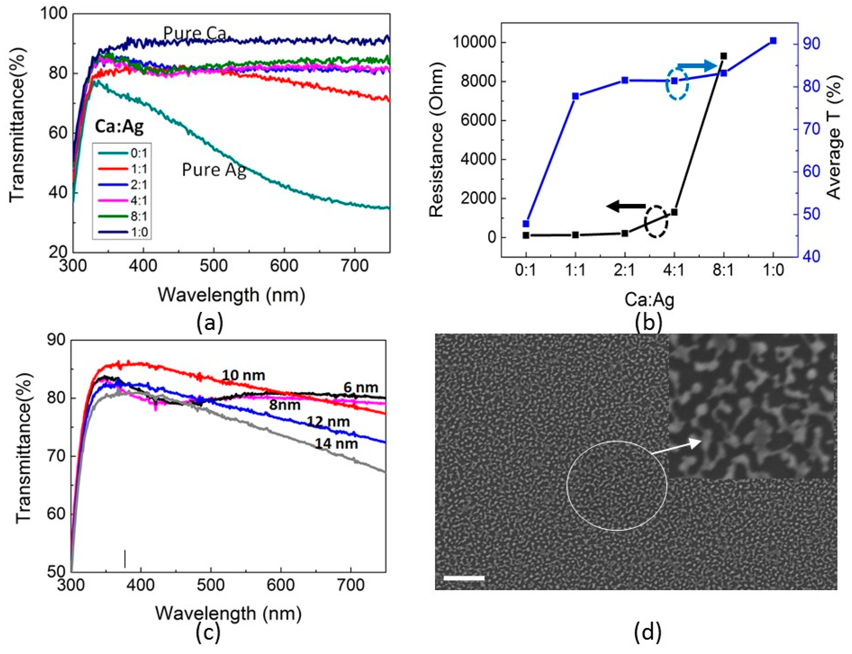
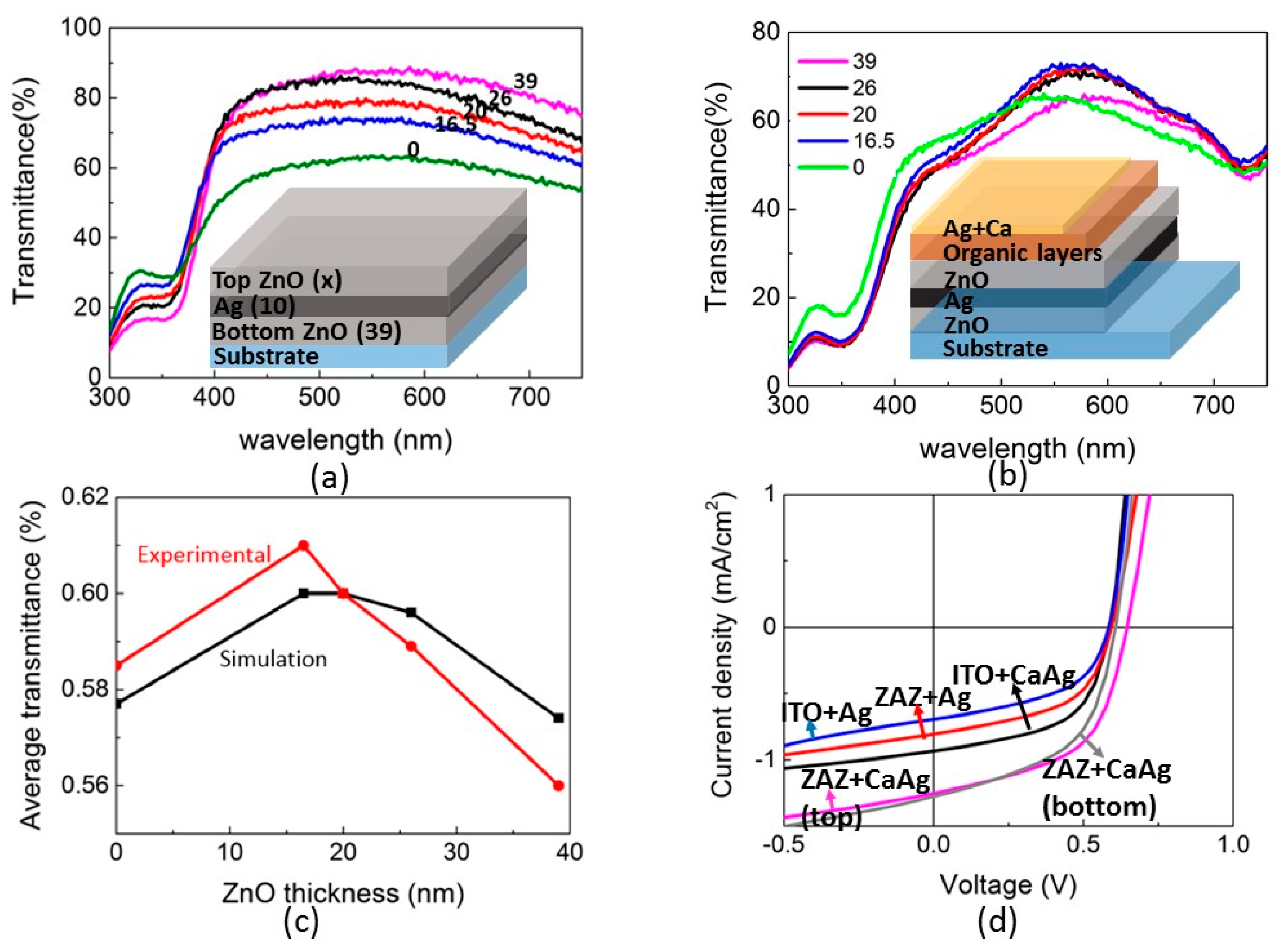
2.3. Transparent Top Electrode

Whereas a small selection of candidates for a transparent bottom contact exist, it is a big challenge to find a suitable transparent top electrode for organic solar cells. The main limitation comes from fabrication compatibility: the organic photoactive layers are soft, thin, and susceptible to chemical damage by high-energy ionic species, and easily solvated by many solvents, meaning that these photoactive layers are thoroughly damaged in a sputter deposition chamber and can be dissolved away during spin coating of a sol-gel electrode precursor solution. Therefore, the ZAZ electrode is not suitable as a top electrode for the transparent solar cells, since the organic layers below the top electrode may be damaged during the sputter deposition process.
Here, we use a physical vapor co-deposited, ultra-thin metal blend layer consisting of Ca and Ag as the transparent conductive top electrode of the solar cell. Usually, pure Ag thin films tend to show relatively high conductivity and low transmittance, especially in the visible region, while Ca thin films show relatively high transmittance >90%, but low conductivity [34]. By blending Ca and Ag together in varying ratios to form 10 nm thick films on 0.5” × 0.5” glass substrates, various transmittance and resistance values can be reached, as Figure 5a,b shows. The transmittance and resistance of 10 nm thick pure Ag and Ca electrodes are also depicted for references. When the Ca:Ag ratio is 2:1, a sheet resistance of 210 Ω is obtained, which is comparable to the value of a pure Ag film; however, unlike pure Ag films, a high mean transmittance of 81.46% in the visible region is observed for the Ca:Ag blend film. Therefore, this metal blend electrode displays both the high transmittance of the pure Ca electrode and the high conductivity of the pure Ag electrode, while being accessible via a simple co-evaporation process. Figure 5c plots the thickness dependent transmittance of the Ca:Ag films. When the film thickness is less than 8 nm, a broad dip is observed around 420 nm in the transmittance spectrum, which is indicative of the localized surface plasmon resonance of the nanoparticles of the discontinuous film [32,35]. When the thickness of the metal blend film is 10 nm, the aforementioned dip disappears. Past 10 nm, the average transmittance continuously decreases, possibly due to the formation of phase separated Ag and Ca islands, whose optical properties are predicted to resemble that of pure Ag and are, therefore, predicted to display low visible wavelength transparency. This hypothesis is confirmed by the SEM image in Figure 5d, which reveals that the Ag islands start connecting to each other and form a conducting film at 10 nm.

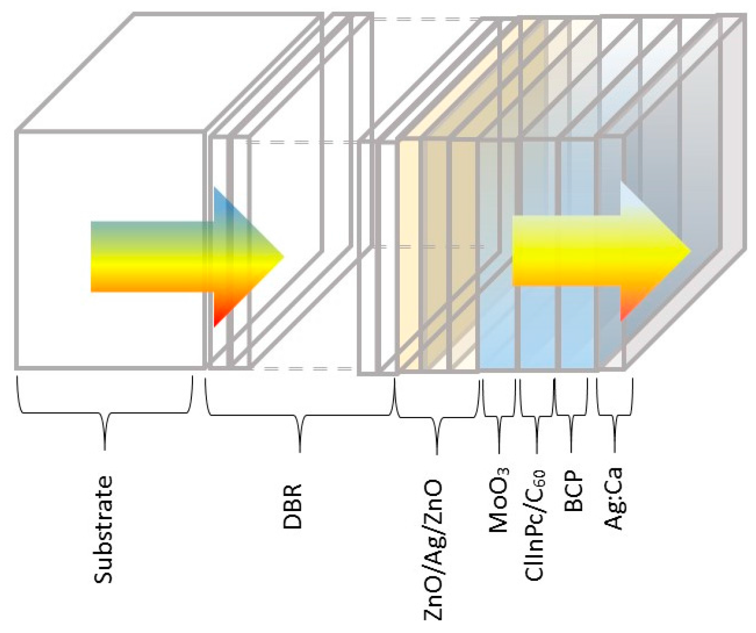
2.4. Transparent Organic Solar Cells

Several research groups have investigated the optical and electrical properties of the ZAZ electrode due to its high flexibility and conductivity. In previous works, the ZAZ electrode has been successfully used as a replacement of ITO in organic solar cells and light-emitting diode (LEDs) [36]. In these studies, most of the attention was paid to increasing the transmittance of the ZAZ multilayer structure. Here, we define the ZnO layer directly deposited on the top of the substrate as the bottom ZnO layer, and the other ZnO layer as the top ZnO layer. The ZAZ electrode can reach its highest transmittance with particular ZnO and Ag thicknesses, as we discussed in the previous section. However, when we combined this high transmittance ZAZ electrode with the aforementioned photoactive organic semiconductors, the transmittance of the whole device is not at the highest value it can reach. In our project, the structure of the transparent solar cell is as follows: glass/ZAZ (39 nm/10 nm/x)/Molybdenum oxide (MoO3) 5 nm/ClInPc 5 nm/C60 13 nm/BCP 5 nm/Ca:Ag (2:1 10 nm). The thickness of ClInPc and C60 were chosen for two reasons. First, in order to achieve the best transmittance of the transparent solar cell, the main light absorber layers of ClInPc and C60 should be as thin as possible. Secondly, since each thin film should be complete without any pinholes to avoid device shorting, the thickness of the thin film could not be too low. Therefore, to attain the balance between device transmittance and device yield, we decided, after testing the solar cells with various thicknesses of ClInPc and C60 layers, to deposit 5 nm ClInPc and 13 nm C60. This combination provides both very thin layers and over 90% device yield. The thickness of the top ZnO layer is varied from 0 to 39 nm. As shown in Figure 6a, the transmittance of the ZAZ electrode increased as the top ZnO layer thickness increases, up to 39 nm. However, after we deposited other organic layers and the top electrode on top of the ZAZ electrode, the transmittance of the completed devices showed totally different trends compared to the plain ZAZ electrode. When the top ZnO layer was 39 nm, even though the ZAZ electrode itself achieved its highest transmittance, the transparent solar cell showed an average transmittance of 57% and a maximum transmission of 66% at 578 nm. When the top ZnO layer is 16.5 nm, however, the complete solar cell reached its highest average transmittance of 60% and a peak transmission over 73% at 556 nm.
To further demonstrate this phenomenon, we wrote an algorithm in MATLAB to tune the thickness of the top ZnO layer and calculate the average transmittance of the transparent solar cell. This program used the transfer-matrix method with refractive index (n) and extinction coefficient (k) values of every organic/inorganic layer as input parameters. We measured the n and k values of each layer by variable-angle spectroscopic ellipsometry. To enhance the accuracy of this simulation, we also considered the reflection of the glass substrate. The simulated average transmittance thus obtained matched the experimental data, with only a 2% difference. Both curves of Figure 6c show the same trend and reached the highest average transmittance when the top ZnO layer had a thickness of 16.5 nm. We conclude that reflective losses arising from the stark difference in n-values at the ZnO-MoO3 interface compared to the ZnO-air interface result in the observed difference in the transmittance of the plain ZAZ electrode versus the completed solar cell. For the ZAZ electrode alone, there are no other layers above the top ZnO layer except for air, whose n value is 1. In a completed device, there are several organic/inorganic layers above the top ZnO layer. Each layer in the device has its own n and k values, which may affect light transport inside of the device. In our transparent solar cells, the n values of MoO3 and organic layers range from 1.75 to 2.3. In this case, when we adjust the structure of the ZAZ electrode, we should consider its optical effect of the whole device, but not only the electrode itself.
Based on all these experiments, a final device structure of glass/ZAZ (39 nm/10 nm/16.5 nm)/Molybdenum oxide (MoO3) 5 nm/ClInPc 5 nm/C60 13 nm/BCP 5 nm/Ca:Ag (2:1 10 nm) was decided upon. Figure 6d and Table 1 show the device performance when this solar cell is top and bottom illuminated by AM 1.5 G illumination with an intensity of 100 mW/cm2. Upon top illumination, the Voc, Jsc, fill factor (FF), and power conversion efficiency (PCE) are 1.25 mA/cm2, 0.65 V, 0.54, and 0.44%, respectively. When bottom illuminated, the Voc, Jsc, FF, and PCE are 1.28 mA/cm2, 0.61 V, and 0.52, and 0.41%, respectively. Both measurements showed very similar performance. These results demonstrate that this device structure can function under top illumination without any performance decrease.
Solar cells with 10 nm Ca:Ag and 15 nm pure Ag as top electrodes were investigated as Figure 6d shows. The device structure of both kinds of solar cells are as follows: ZAZ/MoO3/InClPc/C60/BCP/ top electrode. The Ag electrode solar cell exhibited a Voc of 0.59 V, Jsc of 0.81 mA/cm2, FF of 0.51, and PCE of 0.24%, while the CaAg electrode solar cell had a Voc of 0.65 V, Jsc of 1.25 mA/cm2, FF of 0.54, and PCE of 0.44% by 1 sun, top illumination. The Ca:Ag electrode solar cell achieved higher Jsc because of its higher optical transmittance. Thus, more solar light can penetrate into the absorber layers of the solar cell and generate more excitons. The higher value of FF of the Ca:Ag based solar cell indicates that this metal blend electrode has superior charge collection abilities (with reduced surface recombination) compared to the pure silver thin film electrode. The high conductivity of the top electrode not only improves the device performance by reducing the solar cell series resistance, but also offers the possibility for large scale solar cell manufacturing.
We also used ITO based transparent solar cells as control devices. The ITO electrode was pre-fabricated on glass substrate with the same pattern and size as the ZAZ electrode. The ITO based solar cells showed lower Jsc than the ZAZ based solar cells with the same top electrode by top illumination. The reason is that the ZAZ electrode has higher reflectance in the NIR and UV region than the ITO electrode. Thus more NIR and UV light can reflect back into the active layer of the solar cell for photocurrent generation. The Voc and FF of ITO and the ZAZ electrode based solar cells are similar, which proves that the ZAZ electrode has comparably low sheet resistance, and can be a potential alternative to the ITO electrode.

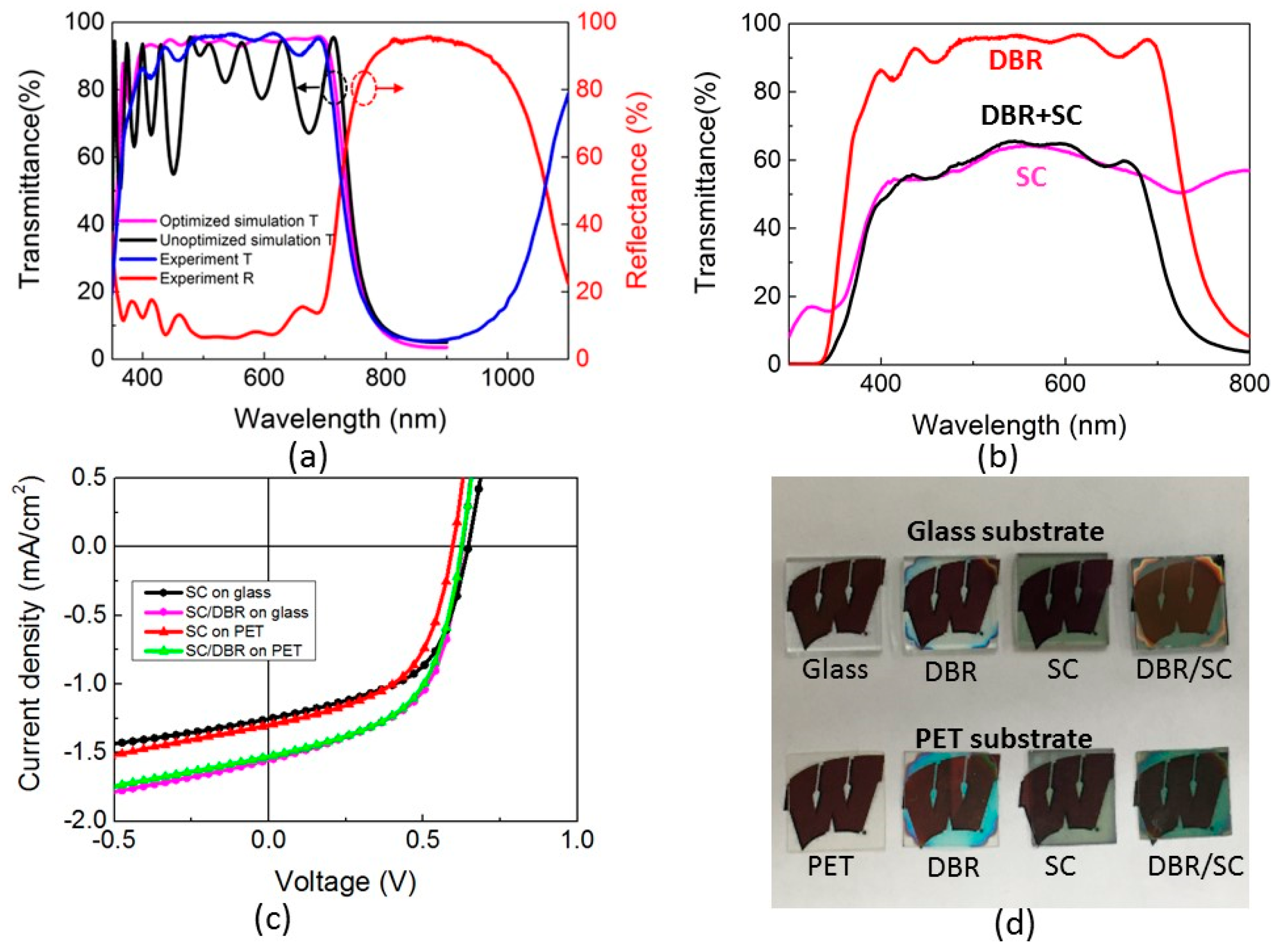
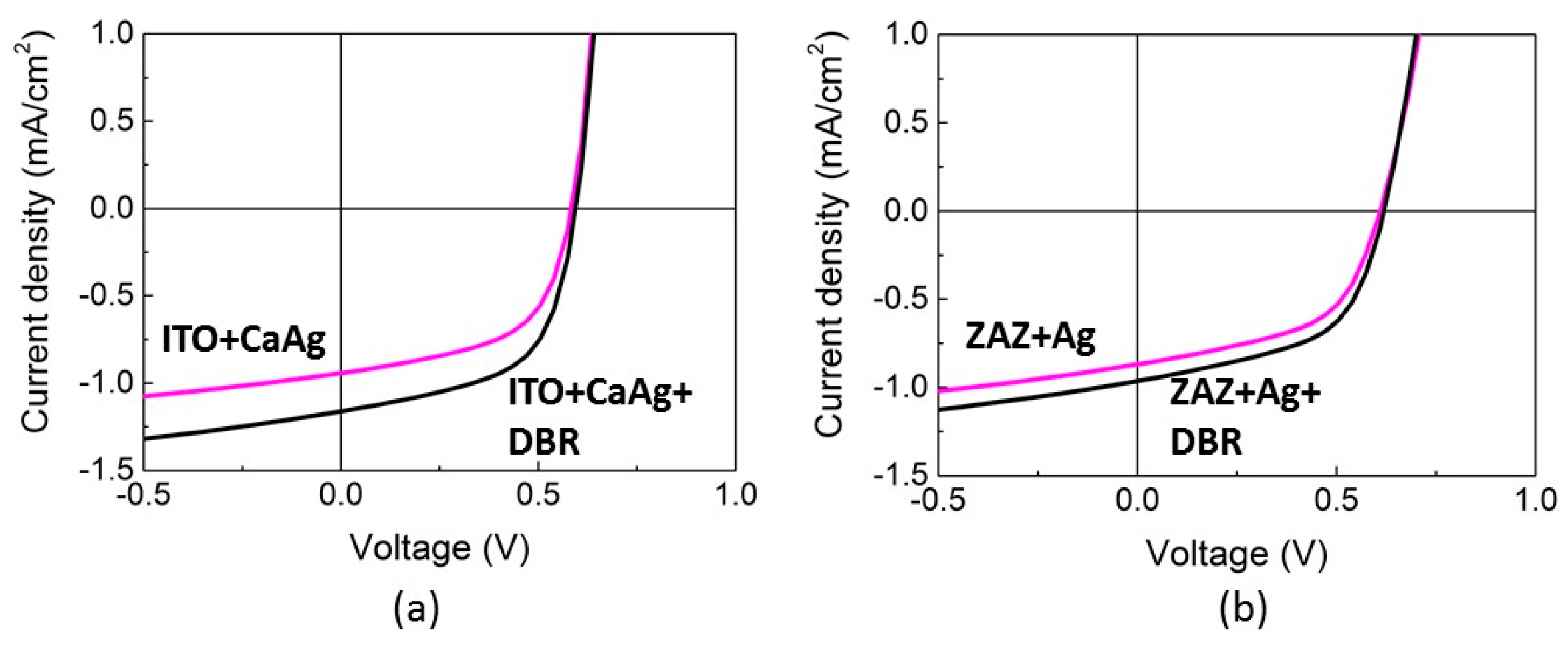
2.5. Adding a Distributed Bragg Reflector to Improve Light Collection and Recycling

A distributed Bragg reflector (DBR) is a highly-reflective small band-pass mirror, which consists of alternating layers of high- and low-refractive-index films [37]. It has high specificity for narrow spectral regions, determined by the thickness and refractive index of the high- and low-refractive-index materials. Here, we used two-material periodic multilayers as a DBR, which is deposited on bottom of the solar cell. We tuned the thickness of each layer to reach a high reflectance at the NIR and UV regions, while maintaining high transmittance in the visible region. We used titanium dioxide (TiO2) and silicon dioxide (SiO2) as the high- and low-refractive-index materials of the DBR, respectively. We used the transfer-matrix method to calculate the exact reflectance region of DBR concerning the light absorption of TiO2, SiO2, and the glass substrate [38]. The refractive index and extinction coefficients of TiO2 and SiO2 over the wavelength regions under study herein are determined by variable-angle spectroscopic ellipsometry [39]. Based on previous research, a DBR layer thickness of one quarter of the center wavelength of the high reflective zone is predicted to cause significant reflectance and reduce transmittance outside the high reflective zone, as Figure 7a shows. In order to avoid reflectance in the visible region, we wrote an automated optimization algorithm with MATLAB. This program tunes the thickness of every layer of the DBR and predicts the reflectance spectrum at each data point. In this case, the layer thickness of the DBR did not equal a quarter of the center wavelength of the high reflective zone, and each layer had a different thickness. The final thickness of each layer of the DBR was: TiO2 86.8 nm/SiO2 147.77 nm/TiO2 78 nm/SiO2 142.31 nm/TiO2 78.16 nm/SiO2 141.72 nm/TiO2 78.87 nm/SiO2 144.25 nm/TiO2 78.47 nm/SiO2 67.23 nm. Figure 7 shows a comparison of the reflectance of a typical 10-layer DBR with a layer thickness a quarter of that of the high reflective zone wavelength, the calculated reflectance of our optimized 10-layer DBR, and experimental reflectance of the DBR we fabricated by RF-sputtering. The wavelength dependent reflection was measured by a spectrometer from 300 to 1100 nm. On one hand, with the structure-optimized DBR coated on the glass substrate, the reflectance of the DBR starts to increase from 700 nm to longer wavelengths, and from 350 nm to its shorter wavelength, which is included in the absorbance region of the active materials of the solar cell. On the other hand, we reached a high average transmittance of 95% in the visible region, and less than 5% transmittance outside of the visible region. Surprisingly, the transmittance of the DBR coated glass device reached an even higher transparency than the uncoated glass substrate in the visible region, since the DBR worked as an anti-reflection layer for the glass substrate. As a result, the DBR works as a NIR mirror, which reflects the light for further absorption of the solar cell, and keeps the solar cell’s high transmission at the same time.
By depositing the DBR on the bottom of the transparent solar cell, the power conversion efficiency increases from 0.44% to 0.53%, which is a 20% increase relative to the efficiency of the transparent solar cell lacking a DBR, and the average transmittance also increases by 0.2% with top illumination. This power conversion efficiency improvement arises entirely from the additional NIR and UV photocurrent in the ClInPc and C60 layers, since only the Jsc shows the same amount of increase but Voc and FF are almost the same as the value of the device without a DBR. The high transmittance of the DBR in the visible region maintains the transmittance of the transparent solar cell. We also deposited a DBR on the bottom of the other transparent solar cells with different kinds of transparent electrodes. All of their power conversion efficiencies improved by 30% as Figure 8 shows. Therefore, the optimized DBR can be successfully applied as a general method to enhance the power conversion efficiency of transparent organic solar cells by reflecting NIR and UV light back to the solar cell without any transmittance loss.
In order to prove that this transparent solar cell is compatible with any kind of substrate, finally, we deposited the transparent solar cell and DBR onto flexible PET substrates. Figure 7c and Table 2 show the device performance of the transparent solar cells with or without DBR on different substrates. The glass based solar cells and the PET based solar cells showed very similar device performance with top illumination. The Jsc of the PET solar cells was slightly higher than the glass solar cell due to the slightly higher reflectance of the PET substrate than the glass substrate. The power conversion efficiency of the PET solar cells increased from 0.41% to 0.54%, with the DBR deposited on the back side of the PET substrate. These results further proved that both our DBR and transparent solar cell have wide applications with different substrates.

3. Discussion

In order to make transparent organic solar cells, the absorption spectra of potential active layer materials need to have valleys in the visible region, between 400 and 700 nm, so that incident light in this region can be transmitted through the device. Furthermore, the active layer materials need to demonstrate sufficiently high absorption in the ultraviolet and infrared regions such that a functional power output can be generated from any resultant solar cells. For these reasons, we chose to investigate chloroindium phthalocyanine as the donor material. This molecular organic semiconductor displays an absorption minimum between 400 and 600 nm and peaks with high absorption cross section in the ultraviolet/near infrared region. As can be seen in the photographs of the completed devices shown in Figure 7d, this choice of active layer materials ultimately resulted in solar cells with average transmittance values of 60% in the visible region.
Furthermore, the intelligent choice of top and bottom electrodes was found to be necessary for producing a functional, high-transmissivity device. Manufacturing concerns were also taken into consideration: many reported examples of transparent electrodes use solution-processing methods whereas the active layer materials investigated herein are deposited using physical vapor deposition under ultrahigh vacuum. A fabrication process flow with both solution-processing and vacuum deposition steps will be slow, expensive, and riddled with defects. Therefore, we narrowed the list of potential transparent electrodes to those that can be deposited via vapor deposition, which lead us to a ZAZ electrode for the bottom contact and Ca:Ag for the top contact. Overall, this device only uses metal oxides that are abundant and globally-available, such as zinc oxide and molybdenum oxide, thus eliminating the need for ITO, the sourcing of which is becoming increasing difficult.
We also demonstrate that our choice of active layer materials and top/bottom electrodes is compatible with any substrate, including flexible plastic substrates. As seen in Figure 7, the solar cells perform similarly on either glass or PET substrates, a feature that is not often observed for many reported organic solar cells. The use of a distributed Bragg reflector increases the performance of both rigid and flexible devices by approximately 30%.
The devices reported herein have the potential to be incorporated into windows in high-rise buildings to harvest energy from incident solar irradiation. Furthermore, and potentially more importantly, the DBR reported herein annihilates device transmissivity past 800 nm, meaning that use of these solar cells in windows will also cool the interior environment during the daytime (due to the loss of warming infrared light).

4. Materials and Methods

ITO-coated glass substrates (Thin Film Devices) were cleaned in M90 (1:400) water solution, DI water, acetone, and isopropyl alcohol (IPA) with sonication for 5 min each. Then the substrates were further cleaned by plasma treatment (300 W) for 10 min. During the manufacturing of the DBR, TiO2 and SiO2 were deposited by an RF sputtering system. Both TiO2 (99.99% purity) and SiO2 (99.99% purity) targets were 3 inch in diameter. The deposition was performed at room temperature in vacuum of 5 mTorr for the pre-sputter and sputter processes. The oxygen and argon flow rates were set as 1:9 respectively for pre-sputtering TiO2 and SiO2. Only argon was injected into the chamber. The pre-sputter process lasted 20 min for both TiO2 and SiO2 with rates of 0.1 Å/s and 0.7 Å/s, respectively. The deposition rate of TiO2 and SiO2 thin films for sputtering were 0.3 Å/s and 1 Å/s, respectively. For the ZAZ electrode deposition, both ZnO and Ag were sputtered onto glass substrates using an RF sputtering system. The diameter of ZnO (99.99% purity) and Ag (99.99 purity) sputter targets were 3 inches. The pre-sputter and sputter of both ZnO and Ag were processed at room temperature in a vacuum of 5 mTorr. The oxygen and argon flow rates were set as 1:9 respectively for pre-sputtering ZnO. Only argon was used for ZnO sputter, Ag pre-sputter, and the sputter process. The pre-sputter process lasted 20 min for both ZnO and Ag with rates of 0.7 Å/s and 1 Å/s. The deposition rates of ZnO and Ag thin films for sputtering were set to 1 Å/s and 2.5 Å/s, respectively. The ZnO and Ag layers were deposited sequentially without vacuum break.
All the solar cells were fabricated on 0.5” × 0.5” large glass substrates. The ZAZ electrode was sputtered on the substrate with a metal shadow mask. All the other layers were deposited by thermal evaporation under ultrahigh vacuum (< 10 6 Torr). MoO3 and the following organic layers were blanket deposited without a vacuum break. The top Ag/Ca electrode was deposited with another metal shadow mask after a vacuum break. The final device area for each solar cell is 1.81 mm2. All device handling and transfer operations, and electrical measurements, were performed in nitrogen filled gloveboxes. Electrical characterizations were performed under dark condition and 1 sum illumination generated by a Newport solar simulator (LCS-100), and the results were not corrected for spectral mismatch. The current density-voltage (J-V) dependence was measured using a Keithley 6487 picoammeter/voltage source. Each device was scanned when the voltage was changed gradually from −0.5 V to 1.5 V and then back to −0.5 V, with a total of 400 points for the cycle. For each kind of solar cell, more than 40 devices were fabricated at the same time. The average value and error value of the device performances were calculated from these devices. The error of the device performance was mostly caused by the non-uniformity of the illumination light during the J-V measurement, and the slight error of the thickness in each layer of the thin film.
Scanning electron microscopy (SEM) images were obtained by using an SEM LEO 1550. Transmittance and reflectance spectra of all films were recorded using an Evolution 220 UV-Visible Spectrophotometer with ISA 220 integrating sphere under transmittance and reflectance modes. Conductivities were calculated from resistivity measurements made using a home-built four-point probe test station. The voltage and current-voltage dependence was measured by a Keithley 2400 source meter. This equipment was programmed with Labview and connected to a lab computer.
To make DBR only highly-refractive in the near IR region and highly-transparent in the visible range, we wrote an automated optimization algorithm in MATLAB to tune the thickness of every layer and obtain the exact transmittance curve we designed. We optimized the thickness of each layer in the DBR structure by minimizing the cost function, which was calculated as the mean squared error between the modeled transmittance and the desired transmittance over the spectrum. We set the desired goal to 100% transmittance in the wavelength region of 400 nm to 700 nm in order to make sure that the DBR multilayer film is highly transparent to visible light. The structure of DBR is 10 layers of alternating SiO2/TiO2 thin films, with glass as the substrate layer and air as the environment. The initial thickness of each layer was set to a quarter of the wavelength in the material. We used 96.5665 nm for the SiO2 layer and 153.0612 nm for TiO2 layer as the initial thickness, respectively. The cost function was minimized by the nonlinear least-squares solver built in MATLAB. To calculate the transmittance of DBR, we used the transfer-matrix method and also took into account the light absorption of TiO2, SiO2, and the substrate glass by introducing the extinction coefficient in the transfer-matrix method. The refractive index (n) and extinction coefficient (k) over light wavelengths of TiO2 and SiO2 were determined by variable-angle spectroscopic ellipsometry. The reflectance of the DBR was calculated as the light perpendicularly hit the surface from the air.

5. Conclusions

In this work, we manufactured a heterojunction transparent organic solar cell with an optimized distributed Bragg reflector. Two kinds of molecular materials, InClPc and C60, were used as donor and acceptor, respectively, since their absorption regions were mostly contained in the UV and NIR regions. We chose a Ca and Ag blend film as the top electrode of the transparent solar cell due to its simple deposition process. The average transmittance of this electrode was over 81% with 10 nm thickness and a Ca:Ag ratio of 2:1. This transparent solar cell used a ZAZ multilayer structure as the bottom electrode, which reached an average transmittance of 78% and peak transmittance of 83% at 578 nm. The resistance of the ZAZ electrode mostly depended on the resistance of the Ag layer, which lead to a low sheet resistance value of 9 ohm/square. The top ZnO layer was adjusted to maximize the average transmittance of the solar cell. As a result, the transparent solar cell reached its best average transmittance of 60%, with a 73% maximum transmittance at 553 nm when the top ZnO layer was 16.5 nm thick. Both the simulated and experimental results agreed with this value. The fully elaborated transparent solar cell devices reached similar performance with both top and bottom illumination, which provides the possibility of using this device on opaque substrates due to the reversal of the illumination direction. We also applied an optimized DBR as the transparent NIR mirror deposited at the back side of the solar cell to improve the current density of the solar cells. The power conversion efficiency of the solar cell increased more than 20% with the DBR without any transmittance loss. In the end, we deposited both the transparent solar cell and the DBR onto the PET substrate. The PET based devices had similar performance as the glass based devices with top illumination, which further widened the application of this device to flexible substrates.

Acknowledgments

The authors gratefully acknowledge financial support from the Air Force Office of Scientific Research (Grant number FA9550-14-1-0128).

Author Contributions

Yuelin Peng, Lushuai Zhang, and Trisha L. Andrew conceived and designed the experiments; Yuelin Peng, Lushuai Zhang, and Nongyi Cheng performed the experiments; Yuelin Peng analyzed the data; Yuelin Peng and Trisha L. Andrew wrote the paper.

Conflicts of Interest

The authors declare no conflict of interest.

References

  1. Tang, C.W. Two-layer organic photovoltaic cell. Appl. Phys. Lett. 1986, 48, 183–185. [Google Scholar] [CrossRef]
  2. Li, G.; Zhu, R.; Yang, Y. Polymer solar cells. Nat. Photonics 2012, 6, 153–161. [Google Scholar] [CrossRef]
  3. Service, R. Solar energy. Outlook brightens for plastic solar cells. Science 2011, 332, 293. [Google Scholar] [CrossRef] [PubMed]
  4. Peng, Y.; Zhang, L.; Andrew, T.L. High open-circuit voltage, high fill factor single-junction organic solar cells. Appl. Phys. Lett. 2014, 105, 083304. [Google Scholar] [CrossRef]
  5. Chen, C.-C.; Dou, L.; Zhu, R.; Chung, C.-H.; Song, T.-B.; Zheng, Y.B.; Hawks, S.; Li, G.; Weiss, P.S.; Yang, Y. Visibly transparent polymer solar cells produced by solution processing. ACS Nano 2012, 6, 7185–7190. [Google Scholar] [CrossRef] [PubMed]
  6. Zhu, R.; Kumar, A.; Yang, Y. Polarizing organic photovoltaics. Adv. Mater. 2011, 23, 4193–4198. [Google Scholar] [CrossRef] [PubMed]
  7. Zhao, Y.; Meek, G.A.; Levine, B.G.; Lunt, R.R. Near-infrared harvesting transparent luminescent solar concentrators. Adv. Opt. Mater. 2014, 2, 606–611. [Google Scholar] [CrossRef]
  8. Starr, C.; Evers, C.; Starr, L. Biology: Concepts and Applications without Physiology; Cengage Learning: Boston, MA, USA, 2010; ISBN 0538739258. [Google Scholar]
  9. Shtein, M. Thin metal films as simple transparent conductors. Int. Soc. Opt. Photonics Newsroom 2009, 10. [Google Scholar] [CrossRef]
  10. Kim, Y.H.; Sachse, C.; Machala, M.L.; May, C.; Müller-Meskamp, L.; Leo, K. Highly conductive PEDOT: PSS electrode with optimized solvent and thermal post-treatment for ITO-free organic solar cells. Adv. Funct. Mater. 2011, 21, 1076–1081. [Google Scholar] [CrossRef]
  11. Leem, D.S.; Edwards, A.; Faist, M.; Nelson, J.; Bradley, D.D.; de Mello, J.C. Efficient organic solar cells with solution-processed silver nanowire electrodes. Adv. Mater. 2011, 23, 4371–4375. [Google Scholar] [CrossRef] [PubMed]
  12. Wang, X.; Zhi, L.; Müllen, K. Transparent, conductive graphene electrodes for dye-sensitized solar cells. Nano Lett. 2008, 8, 323–327. [Google Scholar] [CrossRef] [PubMed]
  13. Schmidt, H.; Flügge, H.; Winkler, T.; Bülow, T.; Riedl, T.; Kowalsky, W. Efficient semitransparent inverted organic solar cells with indium tin oxide top electrode. Appl. Phys. Lett. 2009, 94, 243302. [Google Scholar] [CrossRef]
  14. Zakhidov, A.A.; Lee, J.K.; Fong, H.H.; DeFranco, J.A.; Chatzichristidi, M.; Taylor, P.G.; Ober, C.K.; Malliaras, G.G. Hydrofluoroethers as orthogonal solvents for the chemical processing of organic electronic materials. Adv. Mater. 2008, 20, 3481–3484. [Google Scholar] [CrossRef]
  15. Wu, H.; Kong, D.; Ruan, Z.; Hsu, P.-C.; Wang, S.; Yu, Z.; Carney, T.J.; Hu, L.; Fan, S.; Cui, Y. A transparent electrode based on a metal nanotrough network. Nat. Nanotechnol. 2013, 8, 421–425. [Google Scholar] [CrossRef] [PubMed]
  16. Sahu, D.; Lin, S.-Y.; Huang, J.-L. ZnO/Ag/ZnO multilayer films for the application of a very low resistance transparent electrode. Appl. Surf. Sci. 2006, 252, 7509–7514. [Google Scholar] [CrossRef]
  17. Sahu, D.; Huang, J.-L. High quality transparent conductive ZnO/Ag/ZnO multilayer films deposited at room temperature. Thin Solid Films 2006, 515, 876–879. [Google Scholar] [CrossRef]
  18. El Hajj, A.; Lucas, B.; Chakaroun, M.; Antony, R.; Ratier, B.; Aldissi, M. Optimization of ZnO/Ag/ZnO multilayer electrodes obtained by ion beam sputtering for optoelectronic devices. Thin Solid Films 2012, 520, 4666–4668. [Google Scholar] [CrossRef]
  19. Sahu, D.; Huang, J.-L. Design of ZnO/Ag/ZnO multilayer transparent conductive films. Mater. Sci. Eng. B 2006, 130, 295–299. [Google Scholar] [CrossRef]
  20. Xu, W.-F.; Pan, M.-Y.; Fu, P.-H.; Li, S.-W.; Huang, D.-W.; Wei, P.-K. Efficiency enhancement of top-illuminated ITO-free organic solar cells using plasmonic-assisted nanostructured reflective electrodes. J. Mater. Chem. C 2015, 3, 9131–9136. [Google Scholar] [CrossRef]
  21. Schulze, K.; Uhrich, C.; Schüppel, R.; Leo, K.; Pfeiffer, M.; Brier, E.; Reinold, E.; Baeuerle, P. Efficient vacuum-deposited organic solar cells based on a new low-bandgap oligothiophene and fullerene C60. Adv. Mater. 2006, 18, 2872–2875. [Google Scholar] [CrossRef]
  22. Zhang, L.; Andrew, T.L. Improved photovoltaic response of a near-infrared sensitive solar cell by a morphology-controlling seed layer. Org. Electron. 2016, 33, 135–141. [Google Scholar] [CrossRef]
  23. Liu, X.; Cai, X.; Qiao, J.; Mao, J.; Jiang, N. The design of ZnS/Ag/ZnS transparent conductive multilayer films. Thin Solid Films 2003, 441, 200–206. [Google Scholar] [CrossRef]
  24. Cattin, L.; Bernède, J.; Morsli, M. Toward indium-free optoelectronic devices: Dielectric/metal/dielectric alternative transparent conductive electrode in organic photovoltaic cells. Phys. Status Solidi A 2013, 210, 1047–1061. [Google Scholar] [CrossRef]
  25. Jia, J.; Zhou, P.; Xie, H.; You, H.; Li, J.; Chen, L. Study of optical and electrical properties of TiO2/Ag/TiO2 multilayers. J. Korean Phys. Soc. 2004, 44, 717–721. [Google Scholar] [CrossRef]
  26. Fan, J.C.; Bachner, F.J.; Foley, G.H.; Zavracky, P.M. Transparent heat-mirror films of TiO2/Ag/TiO2 for solar energy collection and radiation insulation. Appl. Phys. Lett. 1974, 25, 693–695. [Google Scholar] [CrossRef]
  27. Choi, K.-H.; Nam, H.-J.; Jeong, J.-A.; Cho, S.-W.; Kim, H.-K.; Kang, J.-W.; Kim, D.-G.; Cho, W.-J. Highly flexible and transparent InZnSnOx∕Ag∕InZnSnOx multilayer electrode for flexible organic light emitting diodes. Appl. Phys. Lett. 2008, 92, 223302. [Google Scholar] [CrossRef]
  28. Kim, J.H.; Na, J.-Y.; Kim, S.-K.; Yoo, Y.-Z.; Seong, T.-Y. Highly transparent and low-resistance indium-free ZnO/Ag/ZnO multilayer electrodes for organic photovoltaic devices. J. Electron. Mater. 2015, 44, 3967–3972. [Google Scholar] [CrossRef]
  29. Kim, H.; Horwitz, J.; Kim, W.; Mäkinen, A.; Kafafi, Z.; Chrisey, D. Doped ZnO thin films as anode materials for organic light-emitting diodes. Thin Solid Films 2002, 420, 539–543. [Google Scholar] [CrossRef]
  30. Todorov, R.; Lozanova, V.; Knotek, P.; Černošková, E.; Vlček, M. Microstructure and ellipsometric modelling of the optical properties of very thin silver films for application in plasmonics. Thin Solid Films 2017, 628, 22–30. [Google Scholar] [CrossRef]
  31. Sreenivasan, M.; Malik, S.; Thigulla, S.; Mehta, B.R. Dependence of plasmonic properties of silver island films on nanoparticle size and substrate coverage. J. Nanomater. 2013, 2013, 90. [Google Scholar] [CrossRef]
  32. Wei, H.; Eilers, H. From silver nanoparticles to thin films: Evolution of microstructure and electrical conduction on glass substrates. J. Phys. Chem. Solids 2009, 70, 459–465. [Google Scholar] [CrossRef]
  33. Crupi, I.; Boscarino, S.; Strano, V.; Mirabella, S.; Simone, F.; Terrasi, A. Optimization of ZnO: Al/Ag/ZnO: Al structures for ultra-thin high-performance transparent conductive electrodes. Thin Solid Films 2012, 520, 4432–4435. [Google Scholar] [CrossRef]
  34. Schubert, S.; Müller-Meskamp, L.; Leo, K. Unusually high optical transmission in Ca: Ag blend films: High-performance top electrodes for efficient organic solar cells. Adv. Funct. Mater. 2014, 24, 6668–6676. [Google Scholar] [CrossRef]
  35. Asanithi, P.; Chaiyakun, S.; Limsuwan, P. Growth of silver nanoparticles by DC magnetron sputtering. J. Nanomater. 2012, 2012, 963609. [Google Scholar] [CrossRef]
  36. Kim, J.H.; Kang, T.-W.; Na, S.-I.; Yoo, Y.-Z.; Seong, T.-Y. ITO-free inverted organic solar cells fabricated with transparent and low resistance ZnO/Ag/ZnO multilayer electrode. Curr. Appl. Phys. 2015, 15, 829–832. [Google Scholar] [CrossRef]
  37. Schubert, M.F.; Xi, J.-Q.; Kim, J.K.; Schubert, E.F. Distributed Bragg reflector consisting of high-and low-refractive-index thin film layers made of the same material. Appl. Phys. Lett. 2007, 90, 141115. [Google Scholar] [CrossRef]
  38. Pettersson, L.A.; Roman, L.S.; Inganäs, O. Modeling photocurrent action spectra of photovoltaic devices based on organic thin films. J. Appl. Phys. 1999, 86, 487. [Google Scholar] [CrossRef]
  39. Lin, H.-W.; Lin, C.-L.; Chang, H.-H.; Lin, Y.-T.; Wu, C.-C.; Chen, Y.-M.; Chen, R.-T.; Chien, Y.-Y.; Wong, K.-T. Anisotropic optical properties and molecular orientation in vacuum-deposited ter (9, 9-diarylfluorene)s thin films using spectroscopic ellipsometry. J. Appl. Phys. 2004, 95, 881–886. [Google Scholar] [CrossRef]
Figure 1. Schematic of the transparent solar cell.
Energies 10 00707 g001
Figure 2. Normalized absorbance of C60 and InClPc thin film. The insets are the molecular structures of C60 and InClPc.
Energies 10 00707 g002
Figure 3. (a) Optical transmittance spectra of Ag thin films with thickness from 1 to 15 nm. (b) Dependence of Ag thickness on its grain size. (c) Dependence of Ag thickness on its sheet resistance. (d) SEM micrographs of the morphology of the Ag thin films.
Energies 10 00707 g003
Figure 4. (a) Transmittance spectra of ZAZ electrodes with various thickness of ZnO layers from 9 to 49 nm. (b) Dependence of sheet resistance of the ZAZ electrode on ZnO thickness. (c) Flexibility test of the ITO and ZAZ electrode.
Energies 10 00707 g004
Figure 5. (a) Transmittance spectra of pure Ca, pure Ag, and the Ca:Ag electrode. (b) Average transmittance of the visible region and sheet resistance of the Ca:Ag electrode. (c) Thin film transmittance of the Ca:Ag electrode with various thickness. (d) Atomic-force microscopy (AFM) image of 10 nm Ca:Ag thin film. The scale bar is 1 µm.
Energies 10 00707 g005
Figure 6. (a) Transmittance spectra of ZAZ electrodes with various thickness of the top ZnO layer. The inset shows the structure of the ZAZ electrode. (b) Transmittance spectra of the transparent solar cells with various thickness of the top ZnO layer. The inset shows the device structure of the transparent solar cells. (c) Experimental and simulated results of the average transmittance of the transparent solar cells with various thickness of the top ZnO layer. (d) J-V curves of the transparent solar cells with different bottom and top electrodes.
Energies 10 00707 g006
Figure 7. (a) Simulated transmittance spectra of unoptimized DBR, optimized DBR, experimental transmittance, and reflectance spectra of DBR with optimized thickness. (b) Transmittance spectra of transparent solar cells with and without DBR. (c) J-V curves of solar cells with and without DBR on glass and PET substrates. (d) Photograph of transparent solar cells and DBR on glass and PET substrates.
Energies 10 00707 g007
Figure 8. Effect of a DBR on the device performance of transparent solar cells with different top and bottom electrodes. (a) Device performance of ITO and Ca:Ag based solar cells with or without DBR. (b) Device performance of ZAZ and Ag based solar cells with or without DBR.
Energies 10 00707 g008
Table 1. Device performance of the transparent solar cells with various electrodes.
Bottom/Top ElectrodeJsc (mA/cm2)Voc (V)FFPCE (%)
ITO/Ag0.69 ± 0.50.58 ± 0.020.48 ± 0.020.19 ± 0.02
ITO/CaAg0.9 ± 0.060.59 ± 0.020.56 ± 0.040.30 ± 0.02
ZAZ/Ag0.81 ± 0.040.59 ± 0.030.51 ± 0.030.24 ± 0.01
ZAZ/CaAg (Top Illumination)1.25 ± 0.060.65 ± 0.030.54 ± 0.020.44 ± 0.03
ZAZ/CaAg (Bottom Illumination)1.28 ± 0.070.61 ± 0.020.52 ± 0.030.41 ± 0.03
Table 2. Device performance of transparent solar cells with DBR and different substrates.
DeviceJsc (mA/cm2)Voc (V)FFPCE (%)
Solar cell on glass1.25 ± 0.040.65 ± 0.020.54 ± 0.030.44 ± 0.02
Solar cell + DBR on glass1.55 ± 0.050.63 ± 0.030.54 ± 0.030.53 ± 0.04
Solar cell on PET1.3 ± 0.070.6 ± 0.020.53 ± 0.040.41 ± 0.03
Solar cell + DBR on PET1.59 ± 0.080.62 ± 0.030.55 ± 0.050.54 ± 0.03

