Switching Device Dead Time Optimization of Resonant Double-Sided LCC Wireless Charging System for Electric Vehicles


Abstract
:1. Introduction
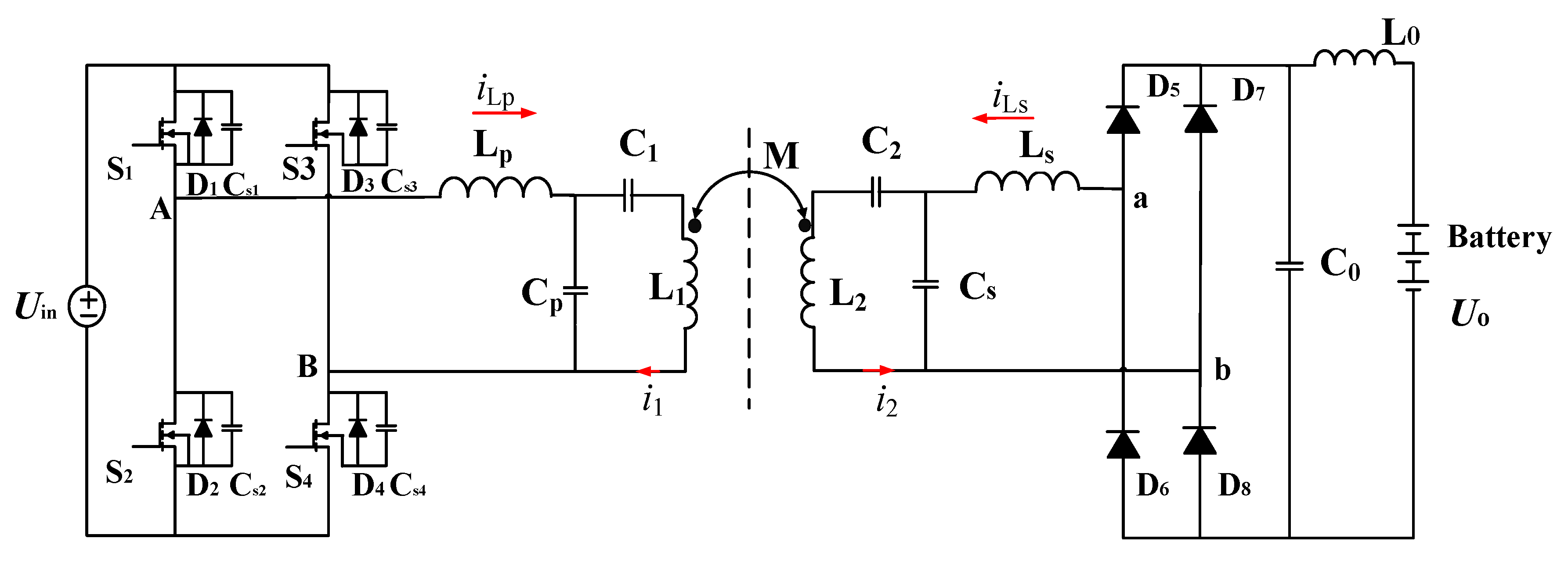
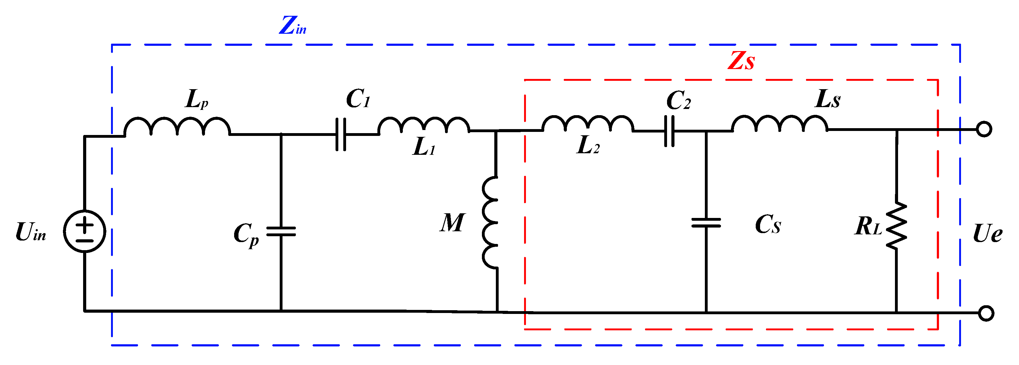
2. Analysis of Double-Sided LCC Resonant Compensation Network Equivalent Characteristic
3. Time Domain Analysis of the Double-Sided LCC Compensation Network
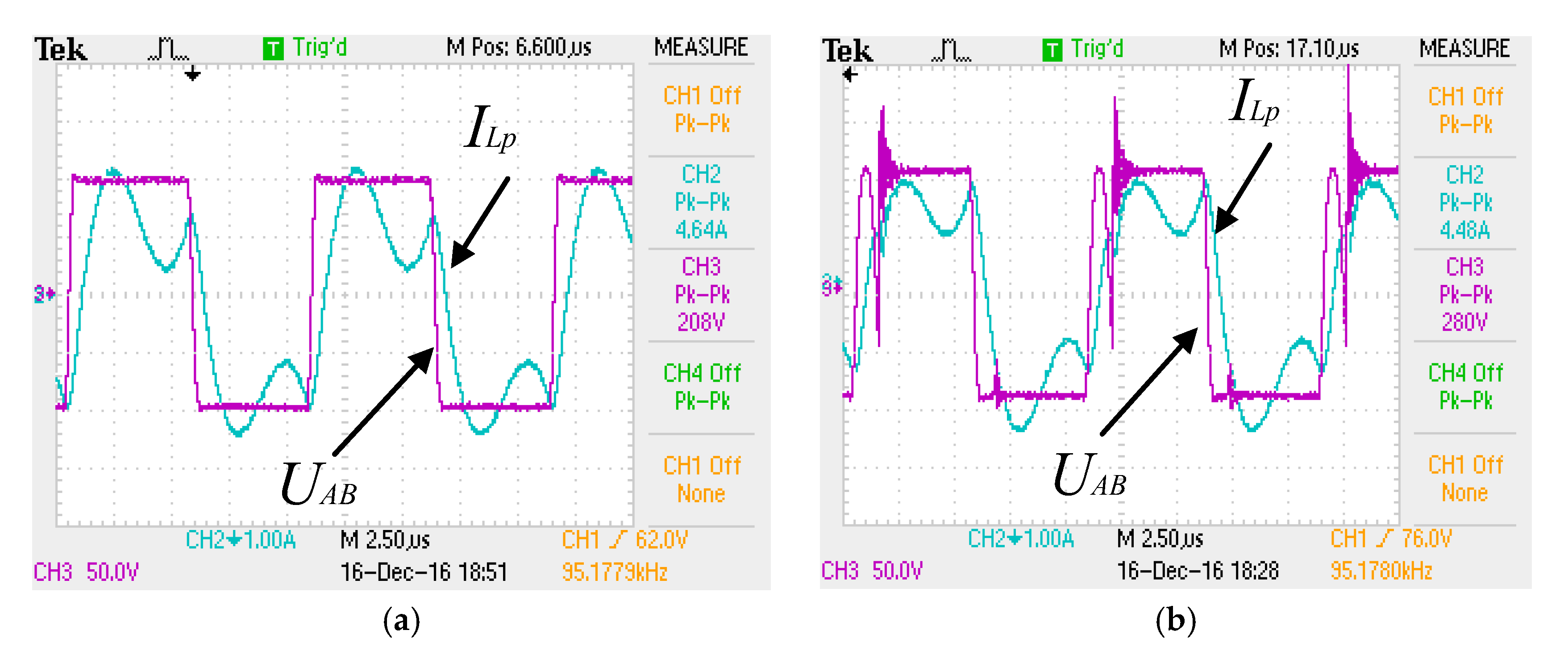
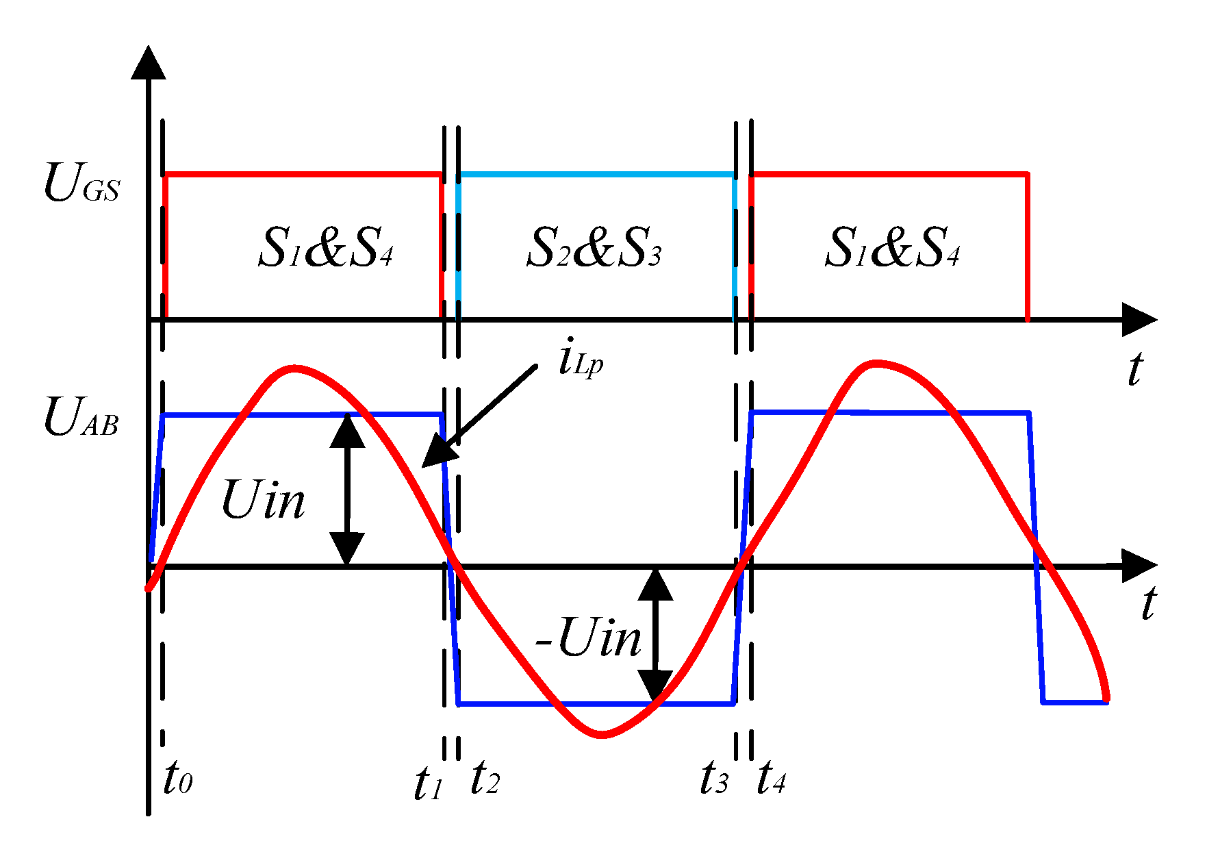
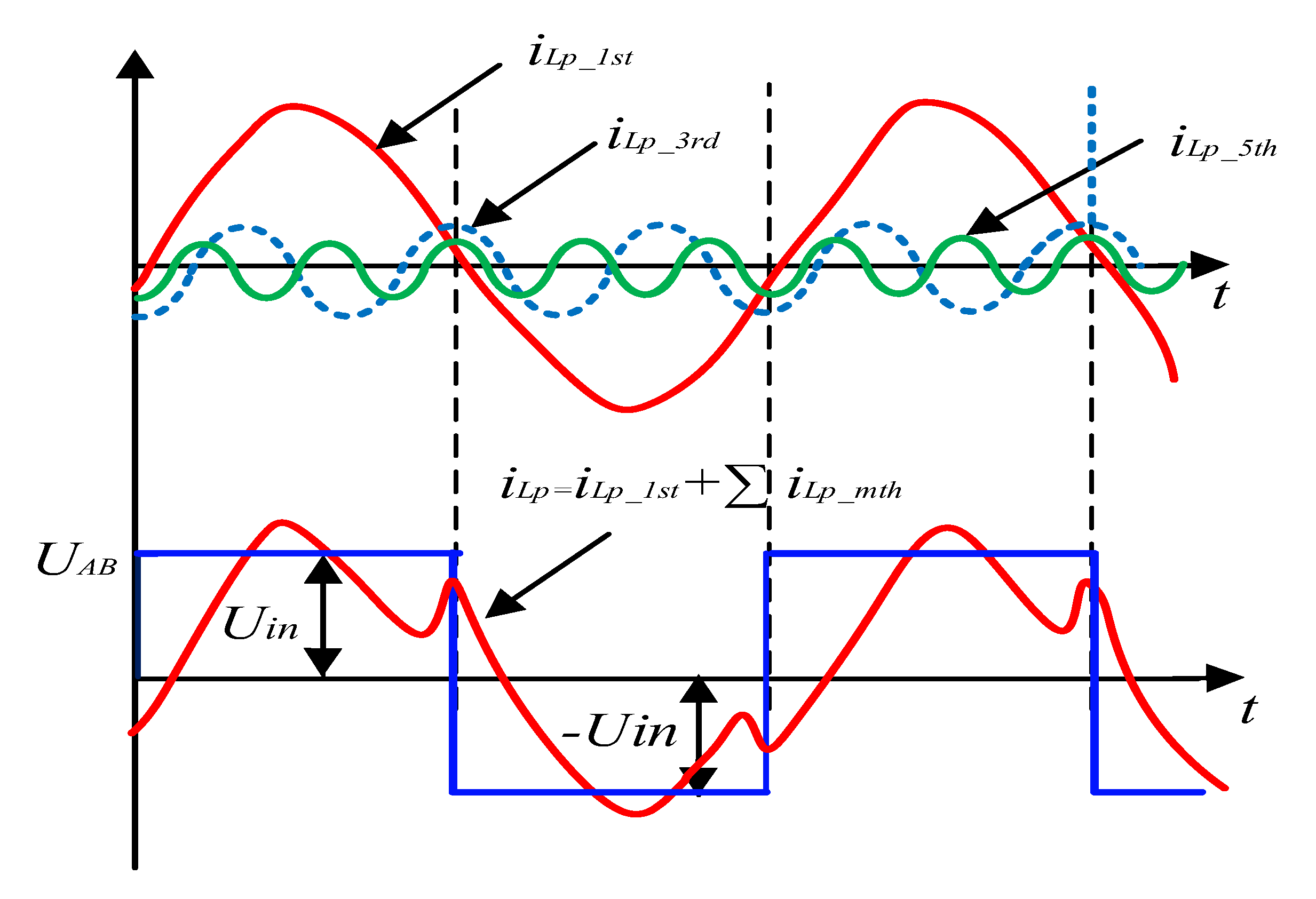
3.1. Time Domain Analysis of Switching Mode
- All the MOSFETs and diodes are ideal;
- All the capacitors, inductors and coils are ideal;
- Cs1 = Cs2 = Cs3 = Cs4 = Coss, where Coss is the output capacitor of the MOSFET;
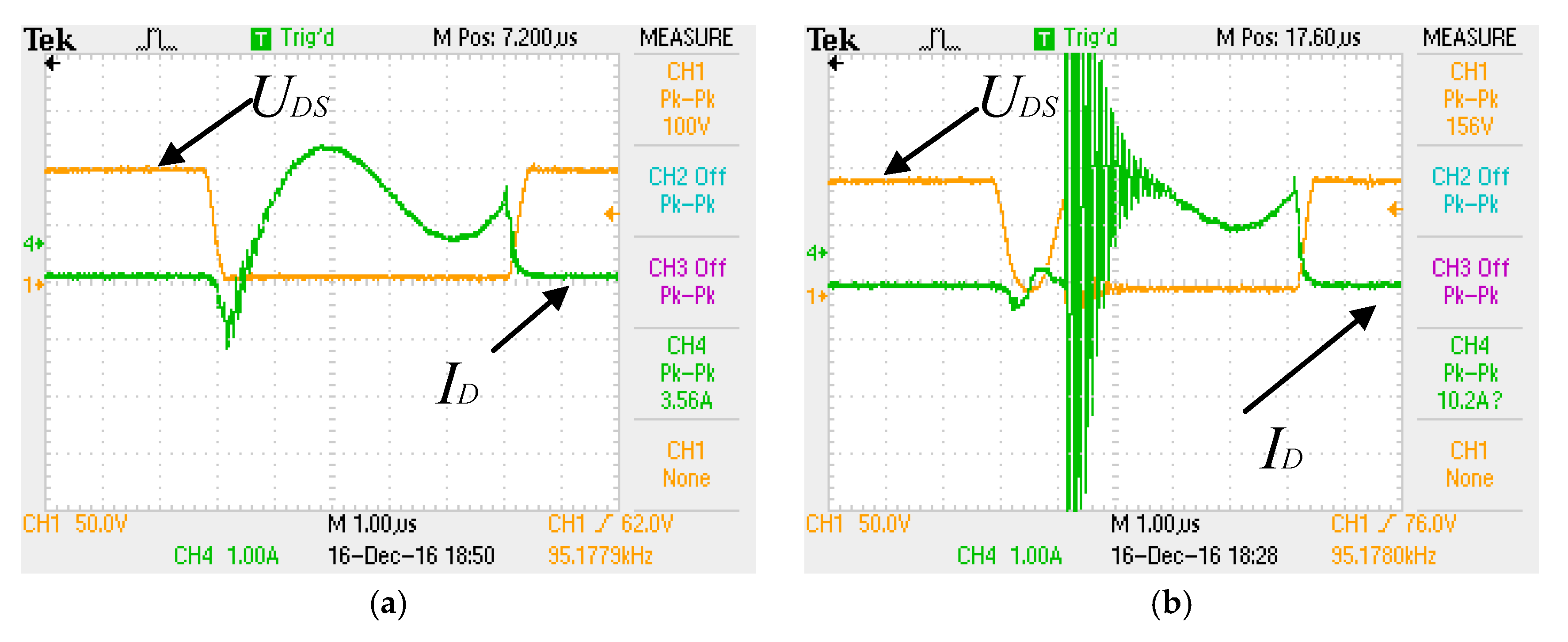
3.2. The Influence of Dead-Time on Soft-Switching
4. Optimization Method of Dead-Time of Inverter MOSFET
4.1. Calculation of Parasitic Capacitor Charging Time
4.2. Calculation of Diode Freewheeling Time
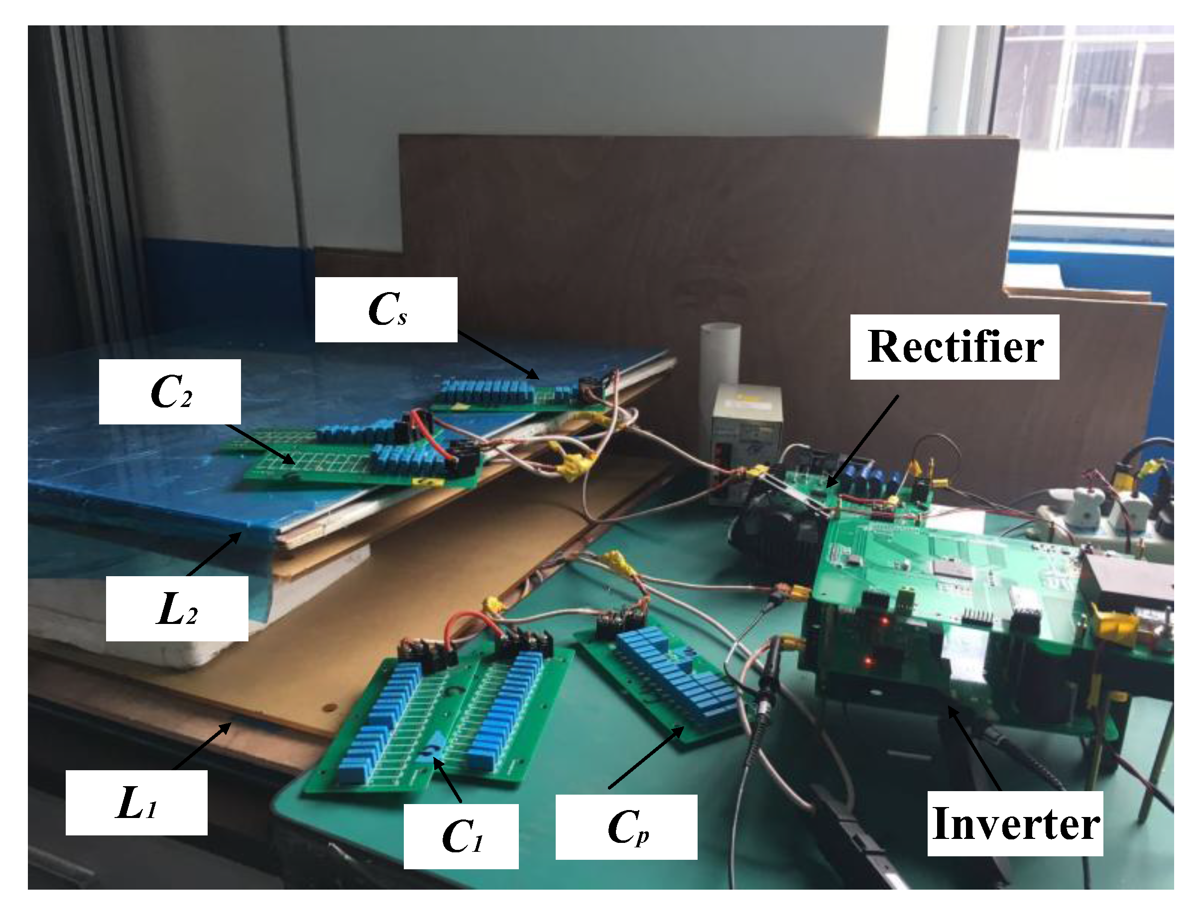
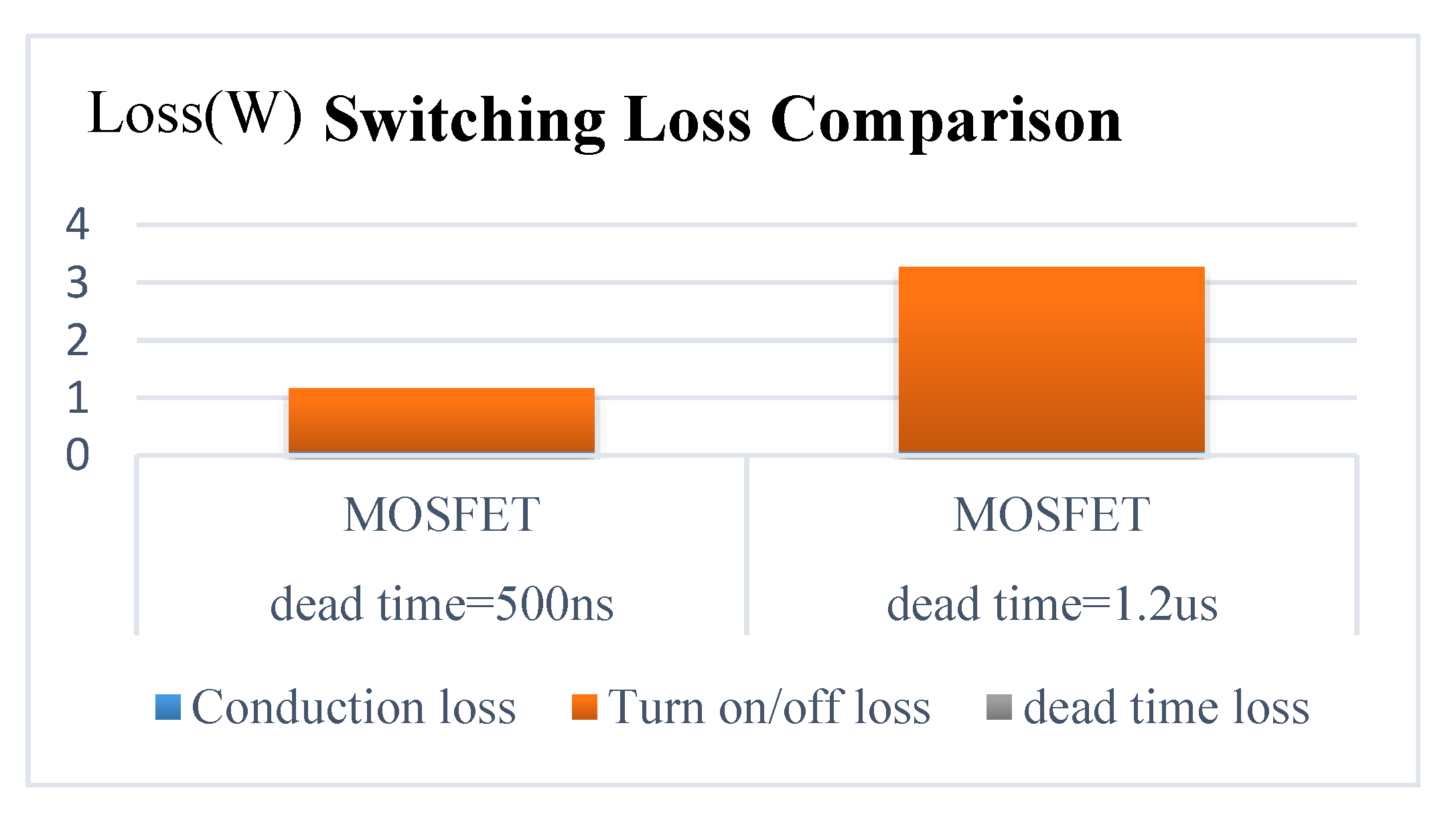
5. Experiment Results
6. Conclusions
Acknowledgments
Author Contributions
Conflicts of Interest
References
- Chen, C.; Xiong, R.; Shen, W. A lithium-ion battery-in-the-loop approach to test and validate multi-scale dual H infinity filters for state of charge and capacity estimation. IET Power Electron. 2018, 33, 332–342. [Google Scholar] [CrossRef]
- Xiong, R.; Yu, Q.; Wang, L.; Lin, C. A novel method to obtain the open circuit voltage for the state of charge of lithium ion batteries in electric vehicles by using H infinity filter. Appl. Energy 2017, 207, 341–348. [Google Scholar] [CrossRef]
- Xiong, R.; Zhang, Y.; He, H.; Zhou, X.; Pecht, M. A Double-Scale, Particle-Filtering, Energy State Prediction Algorithm for Lithium-Ion Batteries. Available online: https://doi.org/10.1109/TIE.2017.2733475 (accessed on 1 November 2017).
- Li, S.; Mi, C.C. Wireless Power Transfer for Electric Vehicle Applications. IEEE J. Emerg. Sel. Top. Power Electron. 2015, 3, 4–17. [Google Scholar]
- Madawala, U.K.; Neath, M.; Thrimawithana, D.J. A Power–Frequency Controller for Bidirectional Inductive Power Transfer Systems. IEEE Trans. Ind. Electron. 2013, 60, 310–317. [Google Scholar] [CrossRef]
- Ning, P.; Miller, J.M.; Onar, O.C.; White, C.P. A compact wireless charging system for electric vehicles. In Proceedings of the 2013 IEEE Energy Conversion Congress and Exposition, Denver, CO, USA, 15–19 September 2013; pp. 3629–3634. [Google Scholar]
- Wu, H.H.; Gilchrist, A.; Sealy, K.D.; Bronson, D. A High Efficiency 5 kW Inductive Charger for EVs Using Dual Side Control. IEEE Trans. Ind. Inform. 2012, 8, 585–595. [Google Scholar] [CrossRef]
- Li, S.; Li, W.; Deng, J.; Nguyen, T.D.; Mi, C.C. A Double-Sided LCC Compensation Network and Its Tuning Method for Wireless Power Transfer. IEEE Trans. Veh. Technol. 2015, 64, 2261–2273. [Google Scholar] [CrossRef]
- Lee, S.; Jung, S.; Huh, J.; Park, C.; Rim, C.T.; Cho, G.H. Robust and efficient synchronous buck converter with near-optimal dead-time control. In Proceedings of the 2011 IEEE International Solid-State Circuits Conference, San Francisco, CA, USA, 20–24 February 2011; pp. 392–394. [Google Scholar]
- Zhang, Z.; Wang, F.; Costinett, D.J.; Tolbert, L.M.; Blalock, B.J.; Lu, H. Dead-time optimization of SiC devices for voltage source converter. In Proceedings of the 2015 IEEE Applied Power Electronics Conference and Exposition (APEC), Charlotte, NC, USA, 15–19 March 2015; pp. 1145–1152. [Google Scholar]
- Liu, C.; Ge, S.; Guo, Y.; Li, H.; Cai, G. Double-LCL resonant compensation network for electric vehicles wireless power transfer: Experimental study and analysis. IET Power Electron. 2016, 9, 2262–2270. [Google Scholar] [CrossRef]
- Hou, J.; Chen, Q.; Wong, S.C.; Tse, C.K.; Ruan, X. Analysis and Control of Series/Series-Parallel Compensated Resonant Converter for Contactless Power Transfer. IEEE J. Emerg. Sel. Top. Power Electron. 2015, 3, 124–136. [Google Scholar]
- Kundu, U.; Yenduri, K.; Sensarma, P. Accurate ZVS Analysis for Magnetic Design and Efficiency Improvement of Full-Bridge LLC Resonant Converter. IEEE Trans. Power Electron. 2017, 32, 1703–1706. [Google Scholar] [CrossRef]
- Zeng, H.; Yang, S.; Peng, F.Z. Design Consideration and Comparison of Wireless Power Transfer via Harmonic Current for PHEV and EV Wireless Charging. IEEE Trans. Power Electron. 2017, 32, 5943–5952. [Google Scholar] [CrossRef]
- López, V.M.; Navarro-Crespin, A.; Schnell, R.; Brañas, C.; Azcondo, F.J.; Zane, R. Current Phase Surveillance in Resonant Converters for Electric Discharge Applications to Assure Operation in Zero-Voltage-Switching Mode. IEEE Trans. Power Electron. 2012, 27, 2925–2935. [Google Scholar] [CrossRef]


| Parameter | Value |
|---|---|
| Transmitting (receiving) coil L1(L2)/uH | 260 |
| Compensation inductor Lp, Ls/uH | 66 |
| Mutual inductor M/uH | 67.6 |
| Parallel capacitor Cp, Cs/nF | 42.3 |
| Primary series capacitor C1/nF | 14.4 |
| Secondary series capacitor C2/nF | 15.4 |
| Output equivalent resistance RL/Ω | 25.8 |
© 2017 by the authors. Licensee MDPI, Basel, Switzerland. This article is an open access article distributed under the terms and conditions of the Creative Commons Attribution (CC BY) license (http://creativecommons.org/licenses/by/4.0/).
Share and Cite
Zhang, X.; Lai, Z.; Xiong, R.; Li, Z.; Zhang, Z.; Song, L. Switching Device Dead Time Optimization of Resonant Double-Sided LCC Wireless Charging System for Electric Vehicles. Energies 2017, 10, 1772. https://doi.org/10.3390/en10111772
Zhang X, Lai Z, Xiong R, Li Z, Zhang Z, Song L. Switching Device Dead Time Optimization of Resonant Double-Sided LCC Wireless Charging System for Electric Vehicles. Energies. 2017; 10(11):1772. https://doi.org/10.3390/en10111772
Chicago/Turabian StyleZhang, Xi, Ziyang Lai, Rui Xiong, Zhe Li, Zhimin Zhang, and Liang Song. 2017. "Switching Device Dead Time Optimization of Resonant Double-Sided LCC Wireless Charging System for Electric Vehicles" Energies 10, no. 11: 1772. https://doi.org/10.3390/en10111772
APA StyleZhang, X., Lai, Z., Xiong, R., Li, Z., Zhang, Z., & Song, L. (2017). Switching Device Dead Time Optimization of Resonant Double-Sided LCC Wireless Charging System for Electric Vehicles. Energies, 10(11), 1772. https://doi.org/10.3390/en10111772