1. Introduction
The combination of Voltage Source Converter (VSC) and Direct Current (DC) transmission technology has attracted the interests of researchers and power grid operators recently. DC transmission system has lower loss and higher capacity than the Alternating Current (AC) system. Although the investment cost of converter station in DC transmission system is much higher than in an AC transmission system, the advantages of the DC transmission system are superior to AC transmission system when the transmission distance is long enough [
1].
As the majority of equipment in existing power grids is AC generators and AC loads, converters are needed among AC and DC system. Another role of converters in DC system is to connect and transmit power between different DC voltage levels, just like transformers in AC system.
Current Source Converter (CSC) and VSC are two basic types of converters widely used in AC/DC systems. Thyristor-valves are usually used in CSC, which relies on AC system to achieve commutation. It is also known as Line Commutated Converter (LCC). VSC adopts fully controlled power electronic devices as basic switches, which shows superiority in rapid and independent control of active and reactive power and ability to feed weak AC system with less risk of commutation failures over LCC [
2,
3].
Given the advantages, VSC-DC technology is regarded as a solution to bulk power transmission over long distances and offshore renewable energy integration. Many VSC-DC based projects have been built around the world in order to integrate offshore wind energy [
4], connect asynchronous AC systems, and power offshore platforms [
5].
Solar energy is one kind of clean and renewable energy, which has been significantly developed in the past decades. There are two patterns of PV generations. The first pattern is dispersed installation with Low Voltage (LV) integration and local consumption, and the second one is large-scale centralized installation with Medium/High Voltage (MV/HV) integration and remote consumption [
6]. Because of the fluctuations of solar energy, VSC-MVDC/HVDC system with rapid power flow control characteristic is usually employed when large-scale PV system is integrating into grids.
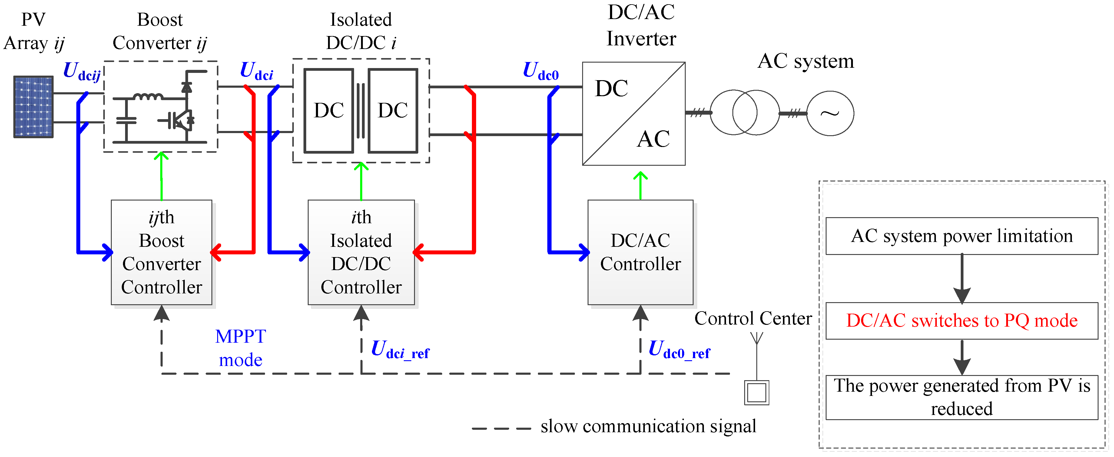
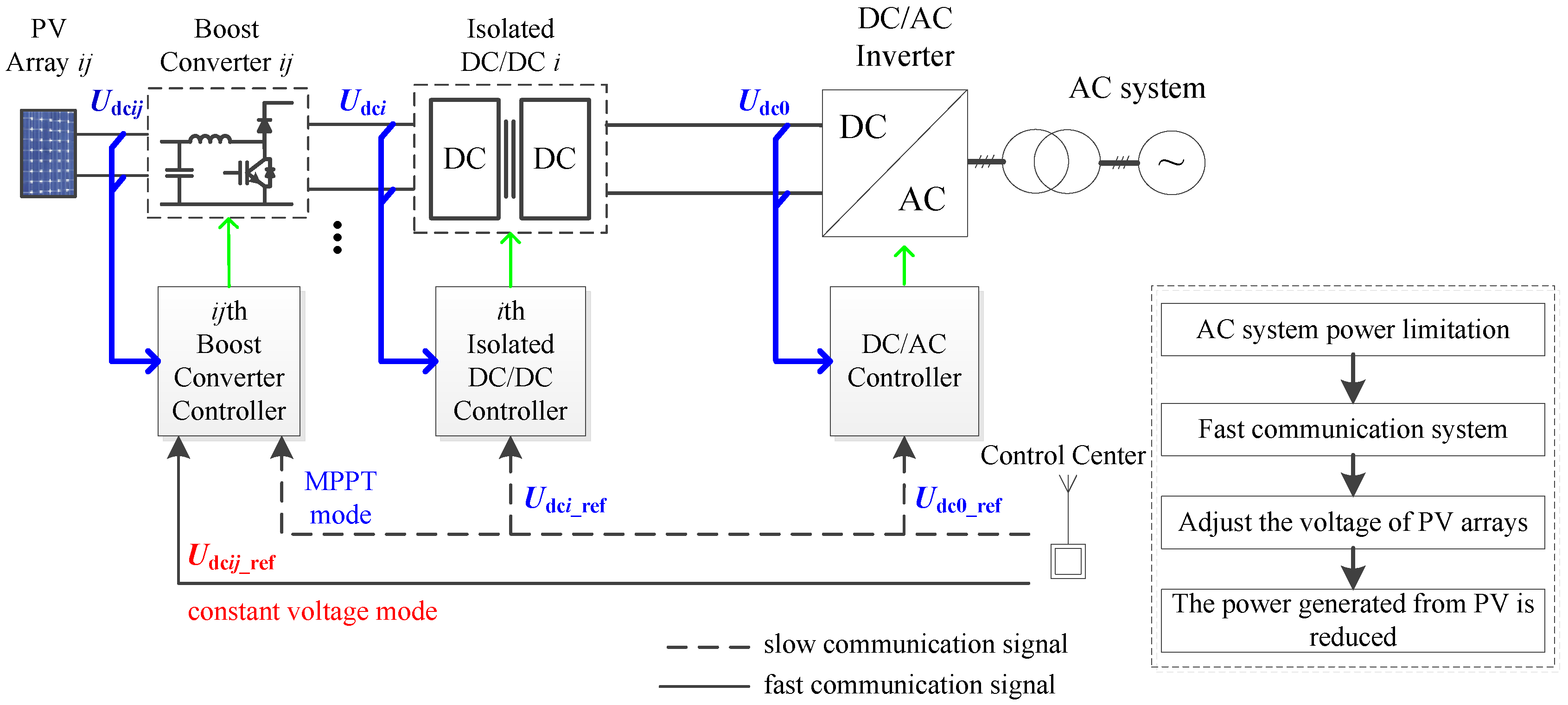
This paper investigates a large-scale concentrating PV system integrated into a power grid with VSC-MVDC (Medium Voltage DC) technology. The power generated by PV arrays is allocated by DC/DC converter, transmitted to load center with MVDC bus, and integrated to AC system with DC/AC converter. There are lots of power electronic devices in VSC-MVDC system. Time domain simulation is very time consuming with the detailed device-level model. Average modeling is an effective method to simplify model complexity so as to accelerate simulation [
7]. Simulation time can be significantly reduced while keeping the same controller structure. It is time-efficient to use the average model when a system-level control is under investigation, in which the dynamic behavior of equipment is not the priority.
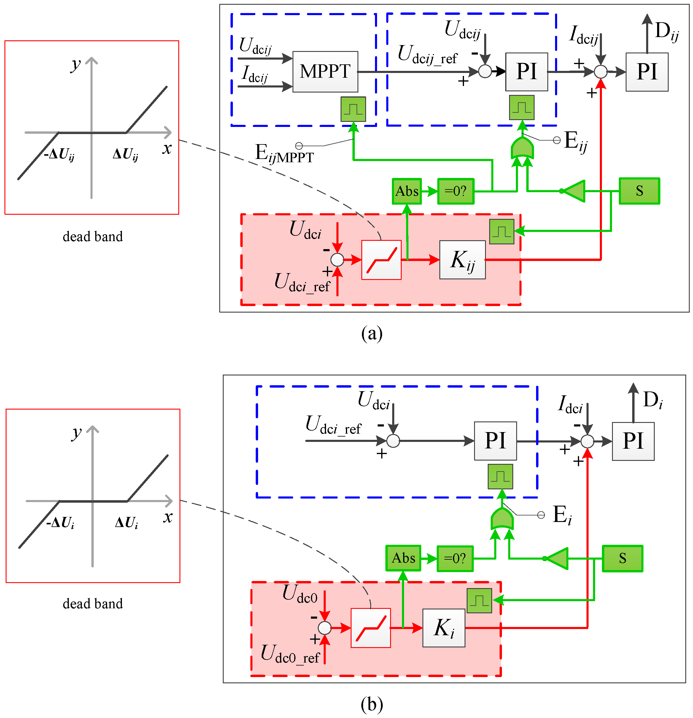
DC voltage is an important indicator of system stability in DC networks. As there are multiple DC voltage buses in the PV-MVDC system, voltages at different DC buses should be controlled coordinately to assure stable and safe operation of the system. An improved coordinated control scheme with a higher system reliability is proposed in this paper, which can keep DC voltages stable under normal operation and power limit conditions without reliance on the fast communication system. The average controlled-source models of converters in PV system are employed to investigate the effectiveness of this control scheme. Time domain simulation results in MATLAB/Simulink indicate the superiority of the proposed control scheme by comparison with the basic conventional control scheme.
2. System Topology and Model
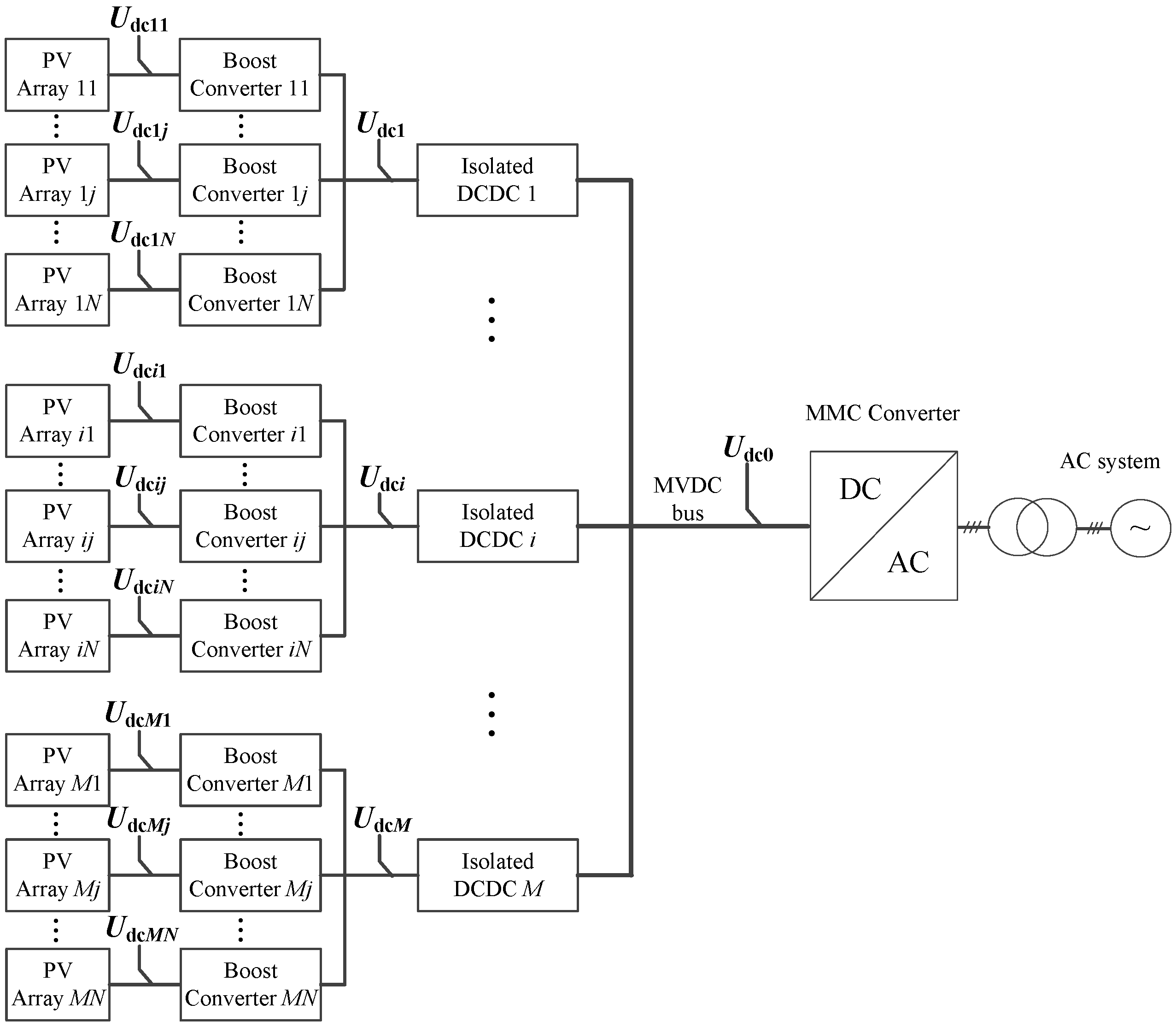
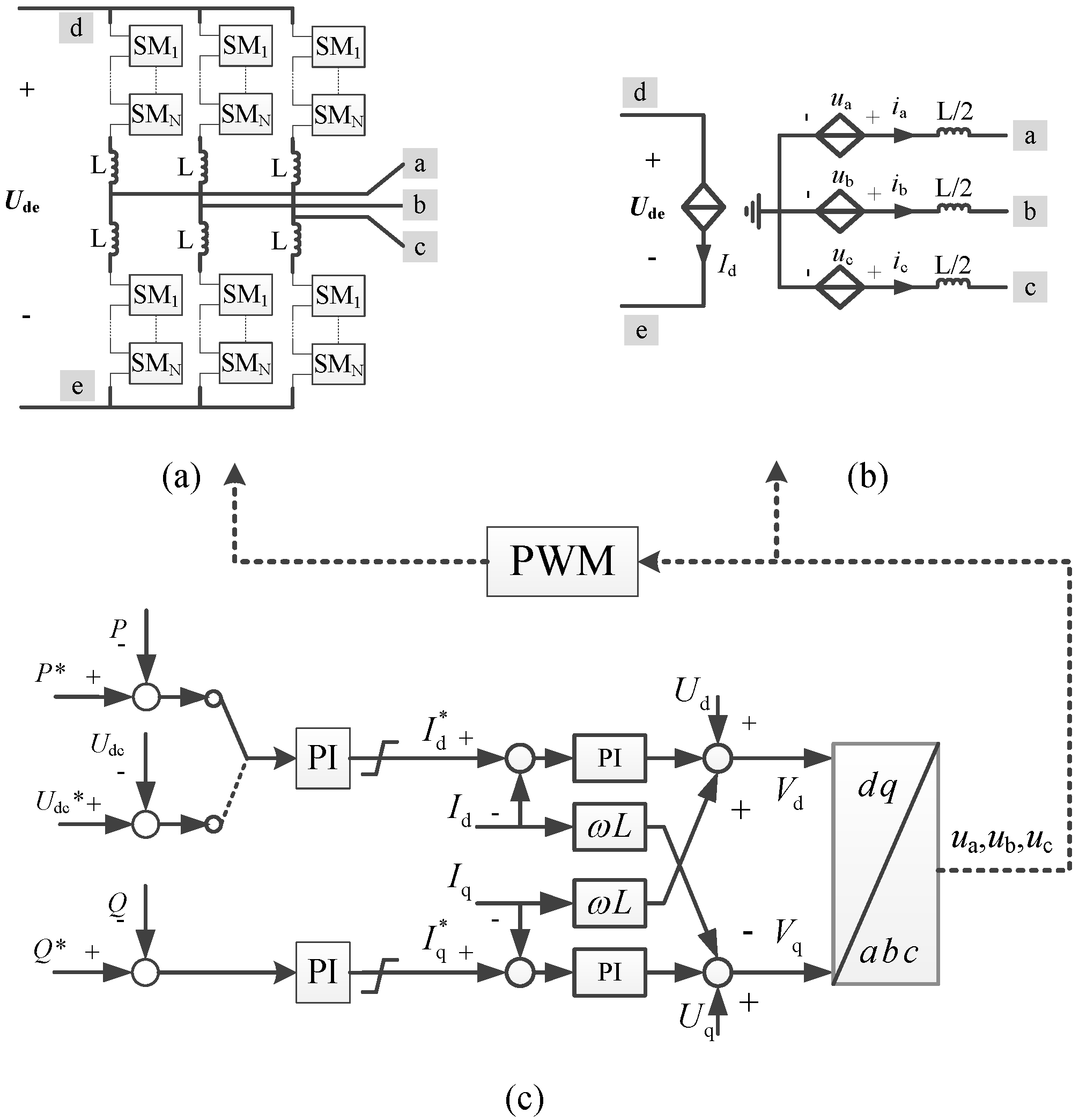
Figure 1 shows the system configuration of a PV integration system. A number of PV panels are connected in series and parallel into a PV array to generate the desired voltage and current. An isolated DC/DC converter is used to step up the voltage. To achieve Maximum Power Point Tracking (MPPT), a boost converter is connected between PV array and isolated DC/DC converter. The MVDC bus allocates the solar power and transmits it to a DC/AC converter to feed AC power system. When two more converters are connected to an MVDC bus, a Multi-Terminal DC (MTDC) system is formed.
In
Figure 1, the number of full-bridge isolated DC/DC converters connected to MVDC bus is
M, and the number of boost converters connected to isolated DC/DC converter bus is
N. The DC voltage at MVDC bus is
Udc0, the DC voltage and current at primary side of
ith full-bridge isolated DC/DC converter is
Udci and
Idci, and the DC voltage and current at primary side of
ijth boost converter is
Udcij and
Idcij. In the following contents, a subsystem composed of the
ijth PV array, the
ijth boost converter, the
ith full-bridge isolated DC/DC converter, the DC/AC converter, and the AC system is selected for analysis and explanations (
i = 1, …,
M,
j = 1, …,
N).
2.1. PV Panel and Boost Converter
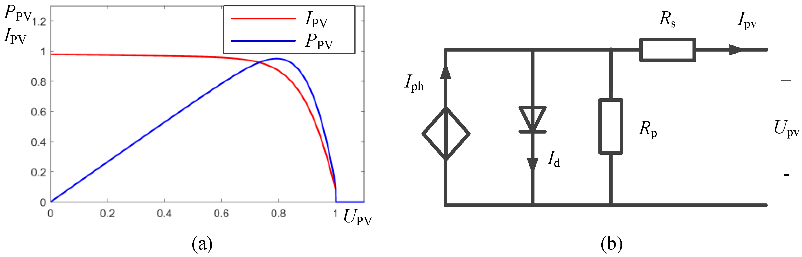
Figure 2 shows the characteristics of PV array and its widely used single diode equivalent circuit model, a combination of an ideal current source sensitive to sunlight, a diode in parallel connection, a parallel resistance
Rp, and a series resistance
Rs [
8]. The relationship between output voltage (
Upv) and current (
Ipv) of PV panel is shown as follows.
where
Iph is the PV current,
I0 is saturation current,
q is the electron charge (1.60217646 × 10
−19 C),
Ns is the number of PV cells in series,
k is the Boltzmann constant (1.3806503 × 10
−23 J/K),
T (in Kelvin) is the temperature, and
A is the diode ideality constant.
As shown in
Figure 2a, there is a Maximum Power Point (MPP) in the power-voltage curve of PV panel. To improve the efficiency of PV panel, a boost converter is used to achieve MPPT. Boost converter acts as an impedance adjuster by changing duty-cycle of the control signal to match PV panel and load impedance under different atmospheric conditions. So far, several MPPT algorithms have been proposed in the literature, and they are categorized into five groups, including tracking techniques with constant parameters, with measurement and comparison, with trial and error, with mathematical calculation, and with intelligent prediction [
9].
Incremental conductance method is used in [
10]. MPP is reached when
dPpv/
dUpv equals to zero, which can be located by comparing the instantaneous conductance (
Ipv/
Upv) to the incremental conductance (∆
Ipv/∆
Upv), i.e.,
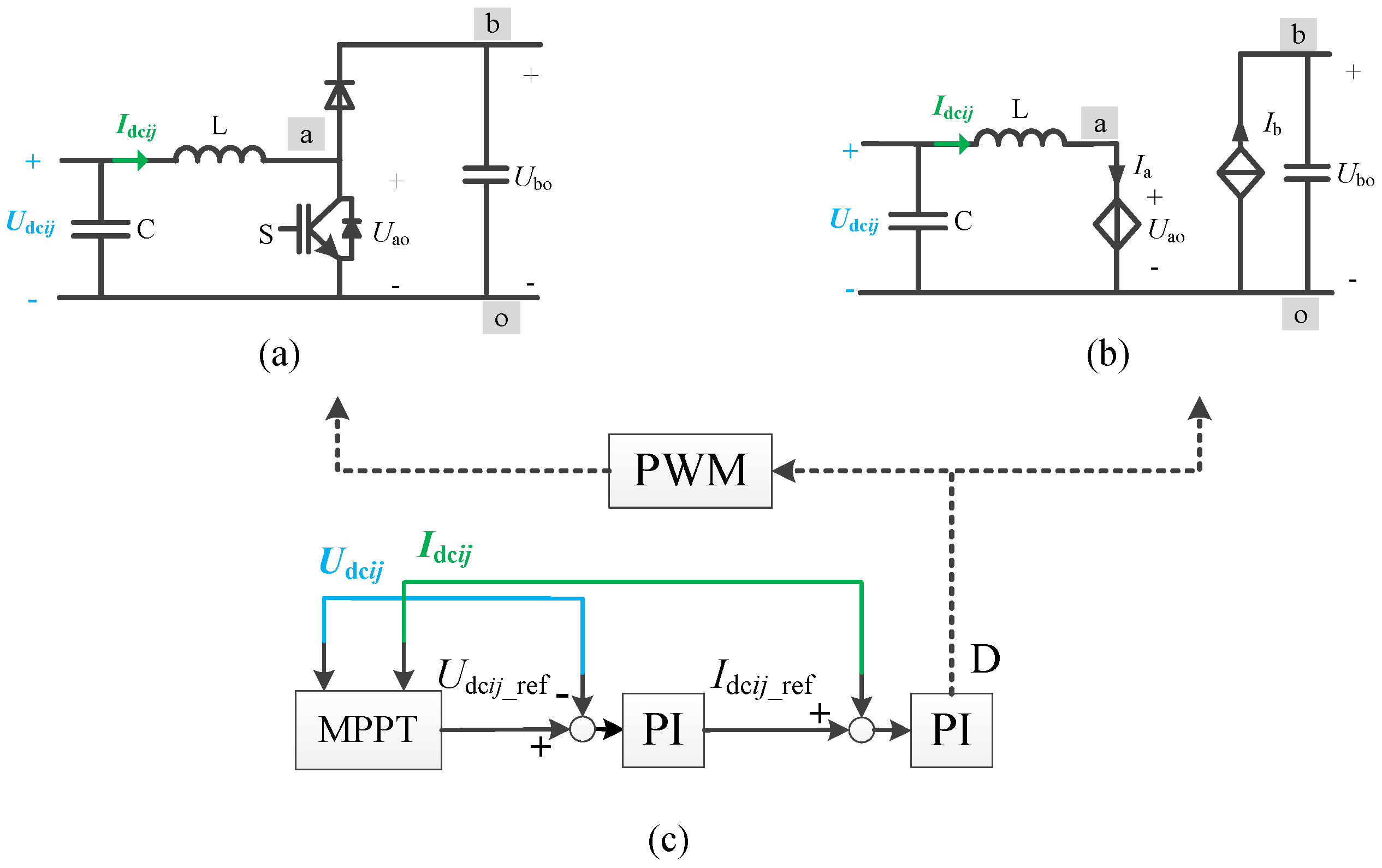
The average model of the boost converter is shown in
Figure 3b, in which a controlled current source and a controlled voltage source are used to replace the complex semiconductor switches. The voltage across semiconductor switch S (
Uao) satisfies
where
Ubo is the output voltage,
Dij is the duty cycle, and
Ts is the period of the carrier.
Power balance formula is the tie of the input side and output side of a boost converter. So the current of the controlled current source (
Ib) is expressed as
where
Ia is the current of the controlled voltage source. The reference direction of these measurements is shown in
Figure 3b.
The controller of the boost converter is shown in
Figure 3c. The reference voltage of PV array,
Udcij_ref, is offered by MPPT controller. The outer voltage controller generates reference current (
Idcij_ref) for the inner current controller, and the inner current controller produces duty cycle of the control signal (
Dij) for the semiconductor switches. For the detailed model, the duty cycle
Dij needs to be transformed into trigger pulses by PWM (Pulse Width Modulation) block. For the average model,
Uao is controlled by
Dij according to function (3).
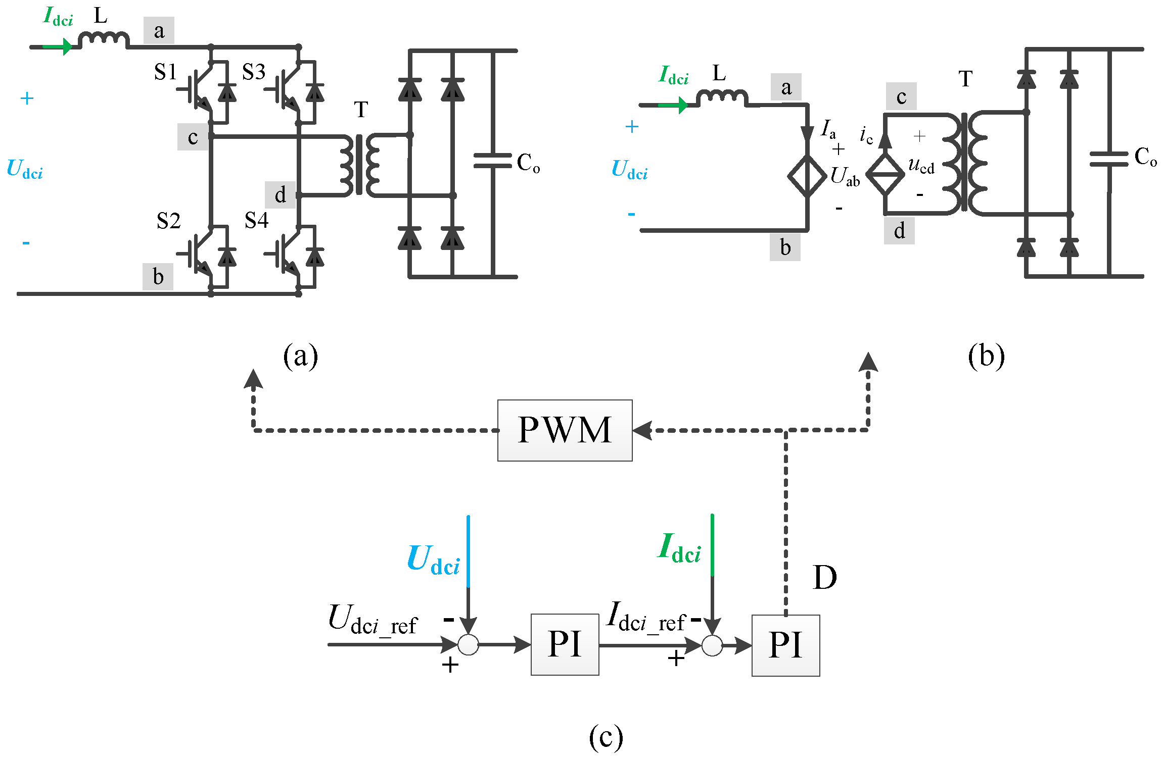
2.2. Full-Bridge Isolated DC/DC Converter
Full-bridge isolated DC/DC converter is used to step up voltage so as to match MVDC bus [
11,
12]. The fully-controlled H-bridge is used to invert DC voltage to AC voltage, the high-frequency transformer is used to provide galvanic isolation and step up voltage, and uncontrolled H-bridge is used to rectify AC voltage to DC voltage, as shown in
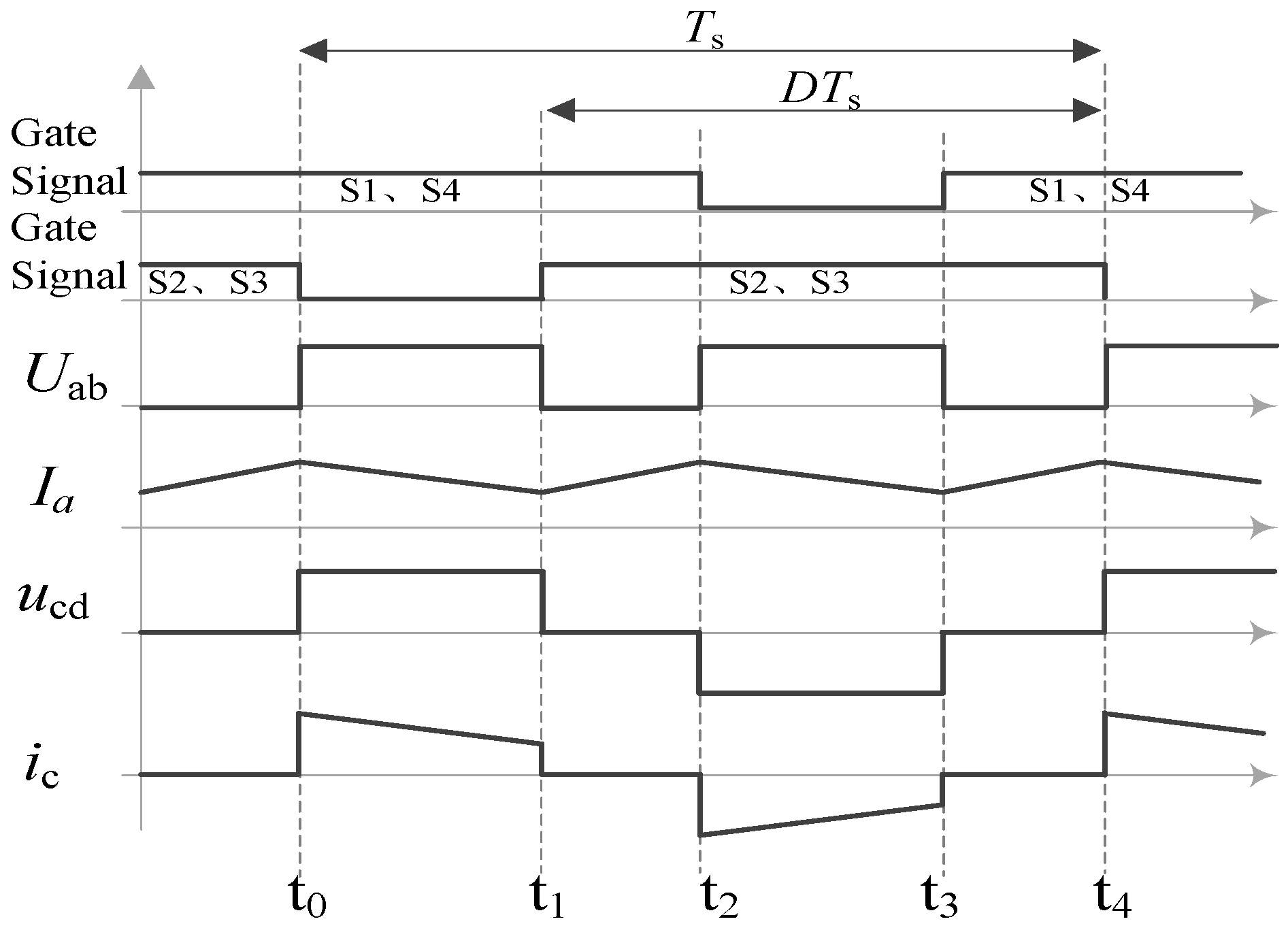
Figure 4. Semiconductor switches S1 and S4 are controlled by identical gating signal, so do S2 and S3. A pair of gating signal shifted by 180° in phase with the duty-cycle greater than 50% is sent to S1 (S4) and S2 (S3). There is an overlap of gating signals of S1 (S4) and S2 (S3), as shown in
Figure 5 (t1~t2 and t3~t4). During this interval, all four switches are inducted on, and energy is stored in inductor L. During t0~t1 (or t2~t3), S2, and S3 (or S1 and S4) are turned off, and the voltage at the primary side of transformer T (
ucd) is boosted.
The current of transformer T at primary side (
ic) is given by
where
Ia is the current of the controlled voltage source and
Di is the duty cycle.
The voltage across a and b,
Uab, is expressed as follows, according to the principle of power conservation. The reference direction of these measurements is shown in
Figure 4b.
The controller of full-bridge isolated DC/DC converter is shown in
Figure 4c, which is similar to the controller of the boost converter in
Figure 3c.
2.3. DC/AC Converter
Modular Multilevel Converter (MMC) is preferred in high power applications for its small converter footprint, high ac-side current quality, and robustness through the use of redundant sub-modules [
13]. Neglecting the complex process of semiconductor switches, the average model of MMC is established, as shown in
Figure 6b.
The controlled voltage source voltage
uj (
j = a,
b,
c) is given by
where
uj_ref is the reference voltage offered by the inner current controller.
The current at DC side (
Id) is expressed as follows, also according to the principle of power conservation.
where
Ude is the voltage of MMC at DC side.
The controller of DC/AC converter is shown in
Figure 6c. To facilitate controller design, the three-phase voltage and current at Point of Common Coupling (PCC) are transformed into dq frame. By selecting different outer controller, DC/AC can operate in
Udc-
Q mode or
P-Q mode. The inner current controller adopts PI controller with current decoupled compensation and voltage feed-forward compensation to compute the reference voltage at converter-side.
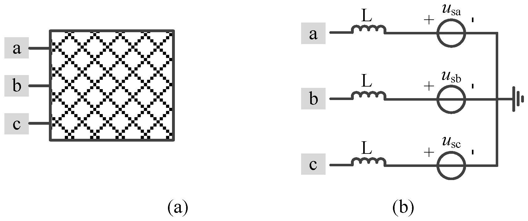
2.4. AC System
AC system is simplified as an ideal three phase voltage source with the specified Short Circuit Level (SCL),
SN, as shown in
Figure 7.
SN is defined as
where
Us and
f are the Root Mean Square (RMS) voltage and frequency of three-phase voltage source at PCC, and
L is the inductance of the internal impedance.
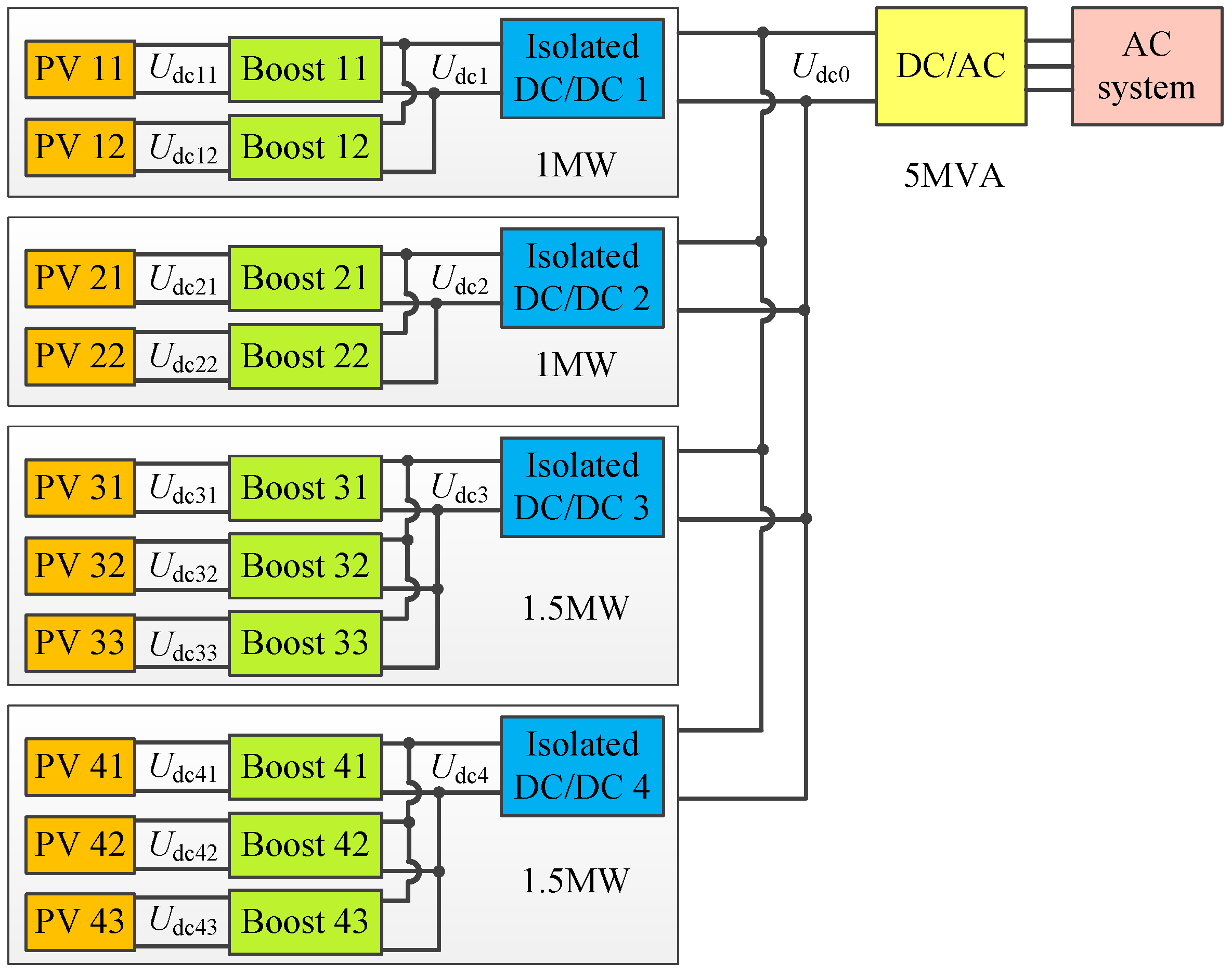
4. Simulation and Results
The average-value model of PV system, as shown in
Figure 11, is established in MATLAB/Simulink to verify the effectiveness of the proposed control strategy. Ten groups of 500 kWp PV panels are connected to ten boost converters, respectively. Four isolated DC/DC converters are connected to an MVDC bus. The power generated by PV panels is integrated into AC grid with one DC/AC converter. The parameters of the modeled system are listed in
Table 1.
The extra voltage loop controllers and MPPT controllers are not effective during 0~6 s (i.e., only basic controller are effective). For this duration, boost converter regulates the voltage at PV panel at 1.035 kV, full-bridge isolated DC/DC converter regulates the voltage at the primary side of isolated DC/DC converter at 2 kV, and DC/AC converter is in Udc-Q mode and regulates MVDC bus voltage at 60 kV.
The extra voltage loop controller and MPPT controller are enabled at 6 s. Boost converter adjusts the voltage at PV panel dynamically to achieve MPPT. The maximum power injected to AC grid is about 4 MW, and DC voltages are kept stable in this process.
DC/AC converter switches into P-Q control mode at 15 s. The power injected to AC grid is limited to 2.5 MW. At 18 s, AC grid needs more active and reactive power support, 3 MW active power, and 1 MVA reactive power are offered from PV system.
The waveform of MVDC bus (
Udc0) and power injected into AC grid (
Pac and
Qac) are depicted in
Figure 12.
Udc0 is regulated at 1 pu during 0~15 s. The power injected into AC grid is smoothly increased to maximum power about 4MW during 6~10 s. When DC/AC converter switches into
P-Q mode at 15 s,
Udc0 will rise and it is a signal to reduce the power generated from PV system.
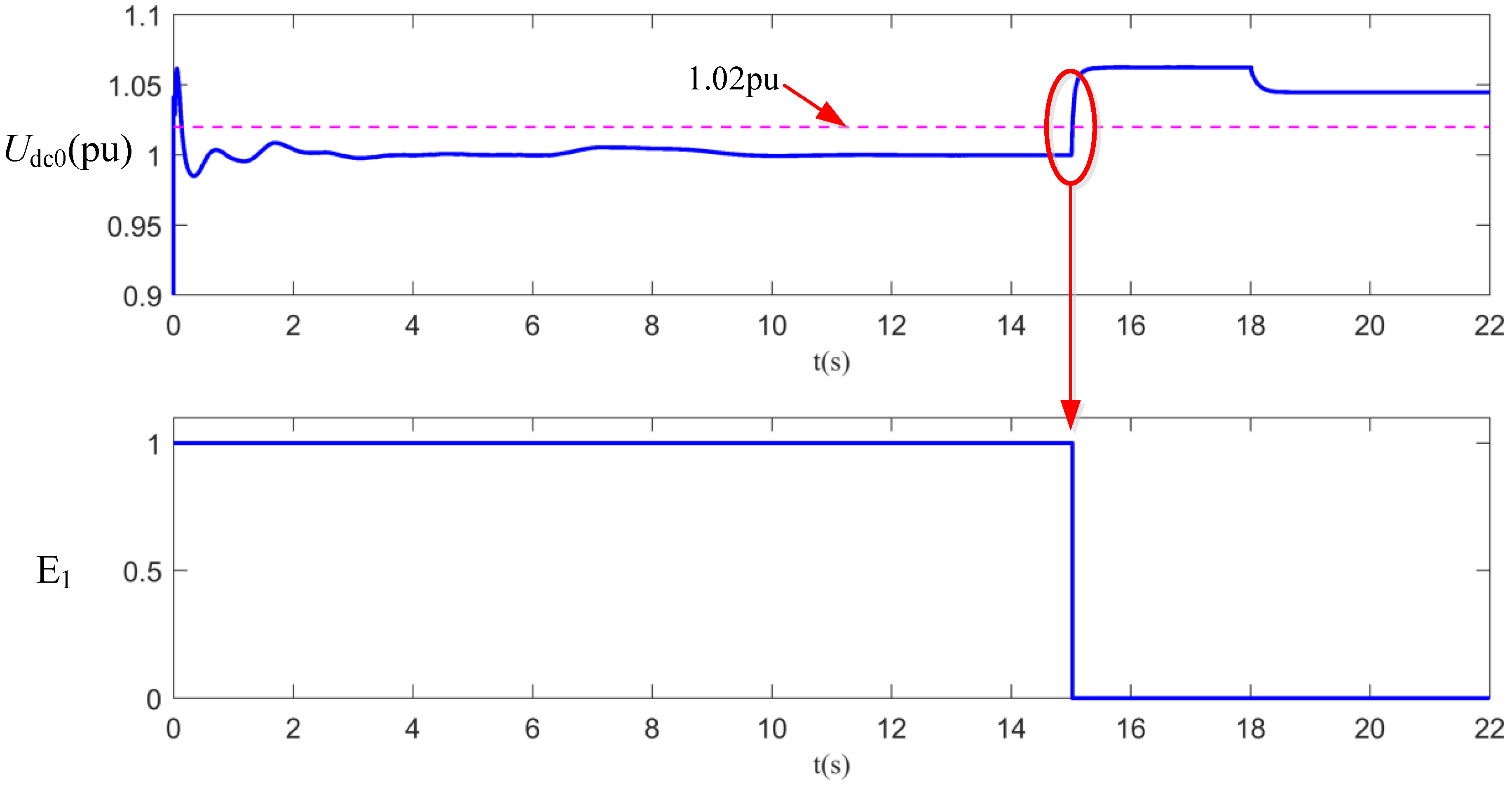
The enable signal of primary side voltage control of full-bridge isolated DC/DC converter 1, E
1, is depicted in
Figure 13. When
Udc0 exceeds the dead band (Δ
U1 = 0.02 pu), E
1 becomes logic zero to disable the primary side DC voltage control of full-bridge isolated DC/DC converter 1. The isolated DC/DC converter 1 is then in control of MVDC bus voltage (
Udc0). The switchover of the controller occurs at 15.02 s when
Udc0 is greater than 1.02 pu.
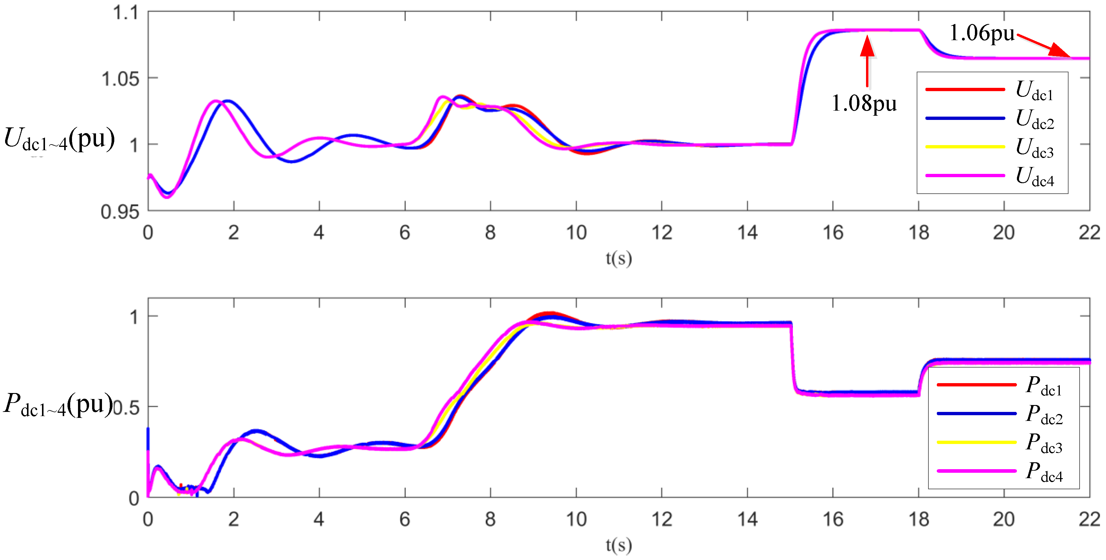
The primary side DC voltage and power waveforms of four isolated DC/DC converters are shown in
Figure 14. The DC voltages,
Udc1~4, are regulated by isolated DC/DC converters at 1 pu during 0~6 s. During 6~22 s, DC voltages,
Udc1~4, are controlled by isolated DC/DC converter 1~4 when they are in the range of 0.97~1.03 pu (the dead band is 0.03 pu). They are controlled by boost converters connected with the isolated DC/DC converter, if DC voltage exceeds the dead band.
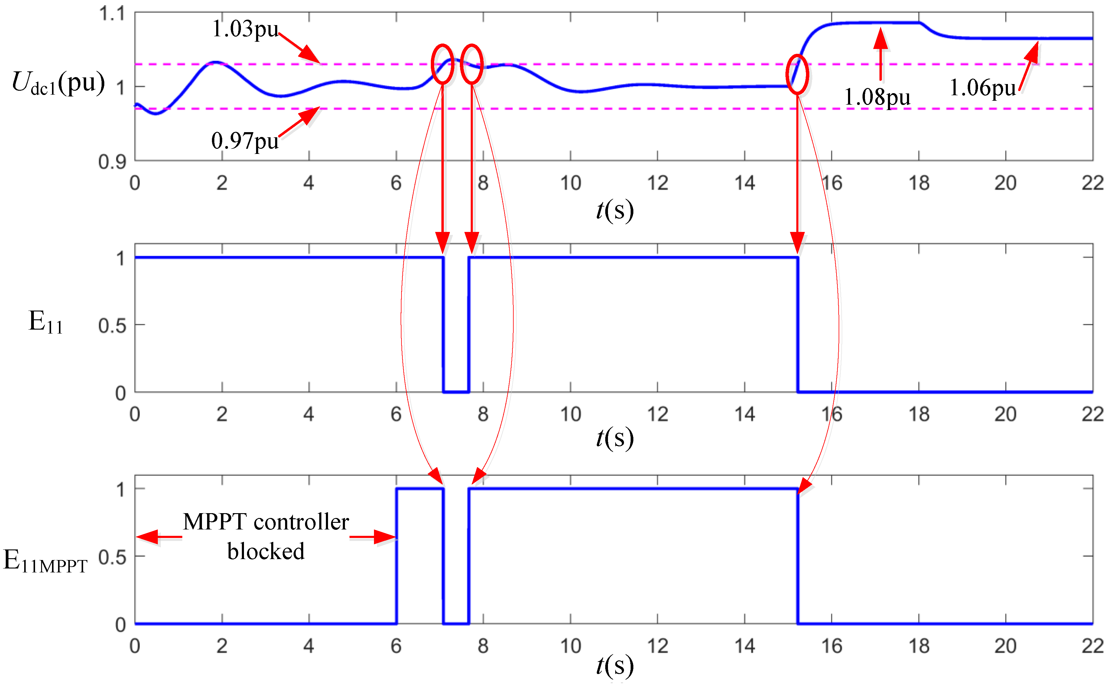
The enable signal of primary side voltage control, E
11, and enable signal of MPPT control, E
11MPPT, of boost converter 11 are depicted in
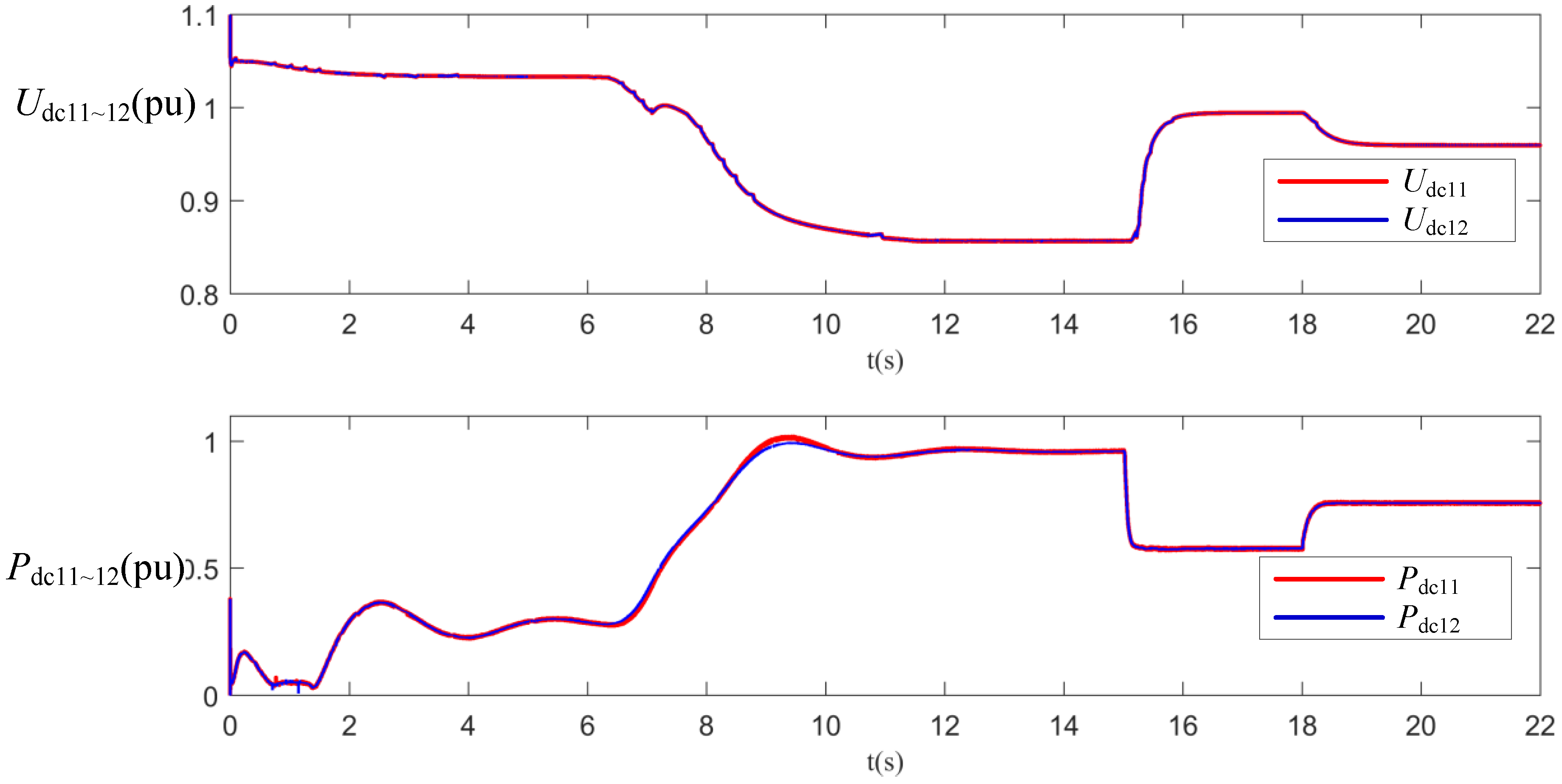
Figure 15. The primary side DC voltage and power waveforms of boost converter 11~12 are shown in
Figure 16. The extra voltage controller and MPPT controller of boost converter 11 are blocked during 0~6 s. The controller of boost converter 11 regulates the voltage at PV panel 11 (
Udc11) at 1.035 pu, which is very close to PV panel’s open circuit voltage (1.05 pu). Extra voltage controller and MPPT controller are unblocked during 6~22 s. The dead band of extra voltage loop in boost converter 11 (Δ
U11) is set to be 0.03 pu. As shown in
Figure 15, E
11 and E
11_MPPT are zero during 7.08~7.66 s, and 15.23~22 s, as the secondary side voltage (
Udc1) of boost converter 11 exceeds 1.03 pu during these periods. The controller of primary side voltage of boost converter 11 is then disabled, and boost converter 11 begins to regulate
Udc1.
Udc1 is stabilized at 1.08 pu during 15~18 s, and at 1.06 pu during 18~22 s. The MPPT controller is also disabled, and PV panels operate at a higher voltage with less power output.
As two or three boost converters are connected to one isolated DC/DC converter, and four isolated DC/DC converters are connected to one DC/AC converter, droop control is used among them to avoid control conflicts. After AC/DC converter switches into P-Q control mode, the MVDC bus voltage rises and it is regulated by isolated DC/DC converter 1~4. The DC voltage at the primary side of isolated DC/DC converter will also rise and be regulated by boost converters. The droop parameter of isolated DC/DC converter 1~4 are all set to be 10, so the power change is equally shared among them. So do boost converter 11~12, 21~22, 31~33, and 41~43.
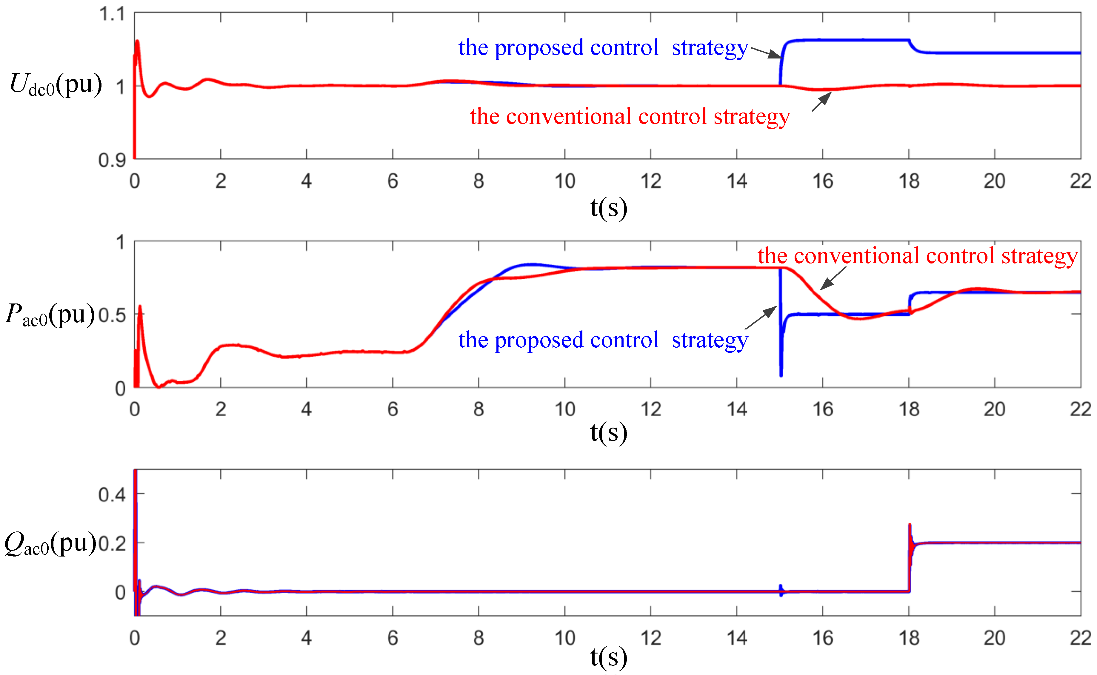
To compare the performance of the improved control strategy and the conventional control strategy, a comparative study is conducted. The communication latency is assumed to be 20 ms, i.e., when DC/AC needs to limit the power at 15 s, a signal to disable MPPT controller and adjust voltage reference at PV panels is sent to the controller of boost converters at 15.02 s. The voltage reference at PV panels is updated at 18.02 s. The waveform of MVDC bus (
Udc0) and power injected into AC grid (
Pac and
Qac) in two cases are depicted in
Figure 17. It is clear that the proposed control strategy has a faster response than the conventional method. Although the DC voltage deviates from 1 pu with the proposed control strategy, it is still in safe range to keep the system in stable operation.


