Article

Enhanced Thermoelectric Properties of Cu3SbSe4 Compounds via Gallium Doping

School of Materials Science and Engineering, University of Jinan, Jinan 250022, China
*
Author to whom correspondence should be addressed.
Energies 2017, 10(10), 1524; https://doi.org/10.3390/en10101524
Submission received: 1 September 2017 / Revised: 17 September 2017 / Accepted: 26 September 2017 / Published: 6 October 2017
(This article belongs to the Special Issue Thermoelectric Materials for Energy Conversion)

Abstract

:
In this study, the p-type Ga-doped Cu3Sb1−xGaxSe4 compounds were fabricated by melting, annealing, grinding, and spark plasma sintering (SPS). The transport properties of Ga-doped Cu3Sb1−xGaxSe4 compounds were investigated. As Ga content increased, the hole concentration of Cu3Sb1−xGaxSe4 compounds increased, which led to an increase in electrical conductivity. Meanwhile, the Seebeck coefficient of the Cu3Sb1−xGaxSe4 compounds decreased as Ga content increased. The extra phonon scattering originating from Ga-doping effectively depressed the lattice thermal conductivity of the Cu3Sb1−xGaxSe4 compounds. The ZT value of Cu3SbSe4 markedly improved, which is primarily ascribed to the depressed lattice thermal conductivity and the increased electrical conductivity. The highest ZT value for the Cu3Sb0.985Ga0.015Se4 compound was 0.54 at 650 K, which is two times higher than that of a pure Cu3SbSe4 compound.

1. Introduction

With the global environmental issue and energy crisis becoming more and more serious, developing renewable and eco-friendly technologies for the sustainable development has gained more attention. Moreover, substantial amounts of waste heat from industrial, private, and transport sectors in modern society should be effectively recovered. Thermoelectric material provides a possibility to solve the issues mentioned above. Thermoelectric material is a kind of energy conversion material, which can realize the conversion between heat energy and electric energy. Thermoelectric material is expected to play a significant role in the field of electronic cooling, power generation, and waste heat recovery. The efficiency of thermoelectric material is usually characterized by the dimensionless figure of merit ZT. The ZT value can be calculated using the equation ZT = σα2T/κ, where κ, T, α, and σ are the total thermal conductivity, absolute temperature, Seebeck coefficient, and electrical conductivity, respectively [1,2,3,4,5]. The total thermal conductivity consists of a carrier part (κc) and a phonon part (κl). Therefore, a large ZT requires the thermoelectric material to have a low κ, a high α, and a high σ. Nowadays, developing high ZT material has been a research focus in the field of thermoelectric materials. As the α, σ, and κe of a material are associated closely with carrier concentration, how to optimize the carrier concentration to realize the maximum ZT is a key issue in this field. To improve ZT, many feasible methods have been developed and applied. Band engineering including electric band structure and valley degeneracy has been regarded as an efficient approach to improve the power factor (PF = α2σ), thereby enhancing the ZT. Doping or nanostructuring are also effective ways of enhancing the ZT by introducing extra phonon scattering centers [6,7,8,9,10].
Recently, copper-based chalcogenide semiconductors have attracted much attention because of their relatively high carrier mobility (μH) and low κ, such as CuGa(In)Te2, Cu2CdSnX4 (X = Se, S), Cu2SnSe3, and Cu3SbSe4 [11,12,13,14]. Among these compounds, ternary Cu3SbSe4 semiconductor has emerged as a promising thermoelectric material because of its narrow band gap and large carrier effective mass. Cu3SbSe4 has a superlattice of a zinc-blended structure and is of the type Cu2FeSnS4 with space group I-42m. The Cu/Se atoms form an electrically conductive framework and the remaining Sb atoms form the one- dimensional [SbSe4] tetrahedra. This special tetrahedra in the Cu3SbSe4 crystal structure can enhance phonon scattering, similar to the “rattling atom” in skutterudite, resulting in a decrease in lattice thermal conductivity. Therefore, Cu3SbSe4 has a relatively low thermal conductivity. However, the electrical properties of intrinsic Cu3SbSe4 is poor due to its low hole concentration (p), which decreases the thermoelectric performance and leads to a low ZT value in the middle temperature range [15,16,17,18]. Theoretically, partial substitution on the Sb site of the Cu3SbSe4 can tune its electrical conductivity so as to enhance the thermoelectric performance. Previous studies about doping on the Sb site have been carried out, and some valuable work has been achieved [19,20]. Qin et al. synthesized the Al-doped Cu3Sb1−xAlxSe4 compounds and the maximum ZT reached 0.58 @ 600 K [21]. Similarly, Ge-doping or In-doping on the Sn site of Cu3SbSe4 was carried out, and the ZT value was enhanced to some extent [22,23]. Gallium has been shown to be a promising dopant in copper-based chalcogenide systems [24], but very little literature on Cu3SbSe4 has been reported. In the present work, the Ga substation on the Sb site is investigated in synthesized Cu3Sb1−xGaxSe4 compounds, and our experimental results demonstrate that Ga-doping can effectively optimize carrier concentration (p) and decrease κ simultaneously. The paper investigated the phase composition, microstructure, and transport properties of Cu3Sb1−xGaxSe4 compounds. The highest ZT of 0.54 was obtained for the Cu3Sb0.985Ga0.015Se4 compound.

2. Experimental Procedures

Cu3Sb1−xGaxSe4 (x = 0, 0.005, 0.010, 0.015) compounds were conventionally synthesized via melting, annealing, grinding, and spark plasma sintering (SPS). The stoichiometric mixtures of pure elements Cu (powder, 99.98%), Sb (powder, 99.998%), Ga (granule, 99.998%), and Se (granule, 99.998%) were loaded in a graphite crucible. Then, the graphite crucible was sealed in a quartz tube, heated to 1173 K, and left for 720 min. The quartz tube was slowly cooled to 773 K at the rate of 0.5 K/min and subsequently quenched in salt water. Then, the sample was annealed at 573 K and the holding time is 48 h to ensure homogeneity. Lastly, the resultant alloys were ground in ethyl alcohol in an agate mortar. The obtained powder was sintered via SPS at 683 K in a vacuum of 0.1 Pa. The axial pressure and holding time were 50 MPa and 5 min, respectively. The Archimedes method was adopted to measure the density (d) of samples.
X-ray diffractometer equipment with Cu Kα radiation (Rigaku Rint 2000) was used to analyze the phase composition of the Cu3Sb1−xGaxSe4 samples. Scanning electron microscopy (SEM, JXA-8200, JEOL, Tokyo, Japan) was employed to characterize the microstructure of Cu3Sb1−xGaxSe4 samples. ZEM-3 apparatus (ULVAC-RIKO, Yokohama, Japan) was used to measure the σ and α in the temperature range of 300–650 K in an argon atmosphere. The measurement of thermal diffusivity (λ) of Cu3Sb1−xGaxSe4 compounds was carried out using a laser flash equipment (Netzsch, LFA427) in an argon atmosphere under a vacuum of 0.001 Pa. A differential scanning calorimetry (Netzsch, DSC404, Munich, Germany) was used to measure the specific heat capacity (Cp) of Cu3Sb1−xGaxSe4 compounds. The thermal conductivity was then obtained by the equation κ = dλCp. Van der Pauw’s method was adopted to measure the Hall coefficient (RH). Hall measurement was carried out in a vacuum of 0.1 Pa with a constant magnetic strength of 0.5 T. The p can be calculated using the equation pH = 1/(RHe), where e is the electron charge. The μH was obtained using the equations of μH = RHσ.

3. Results and Discussion

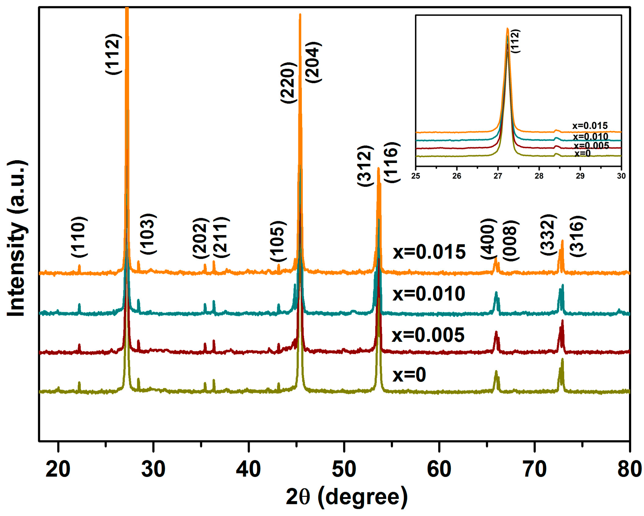
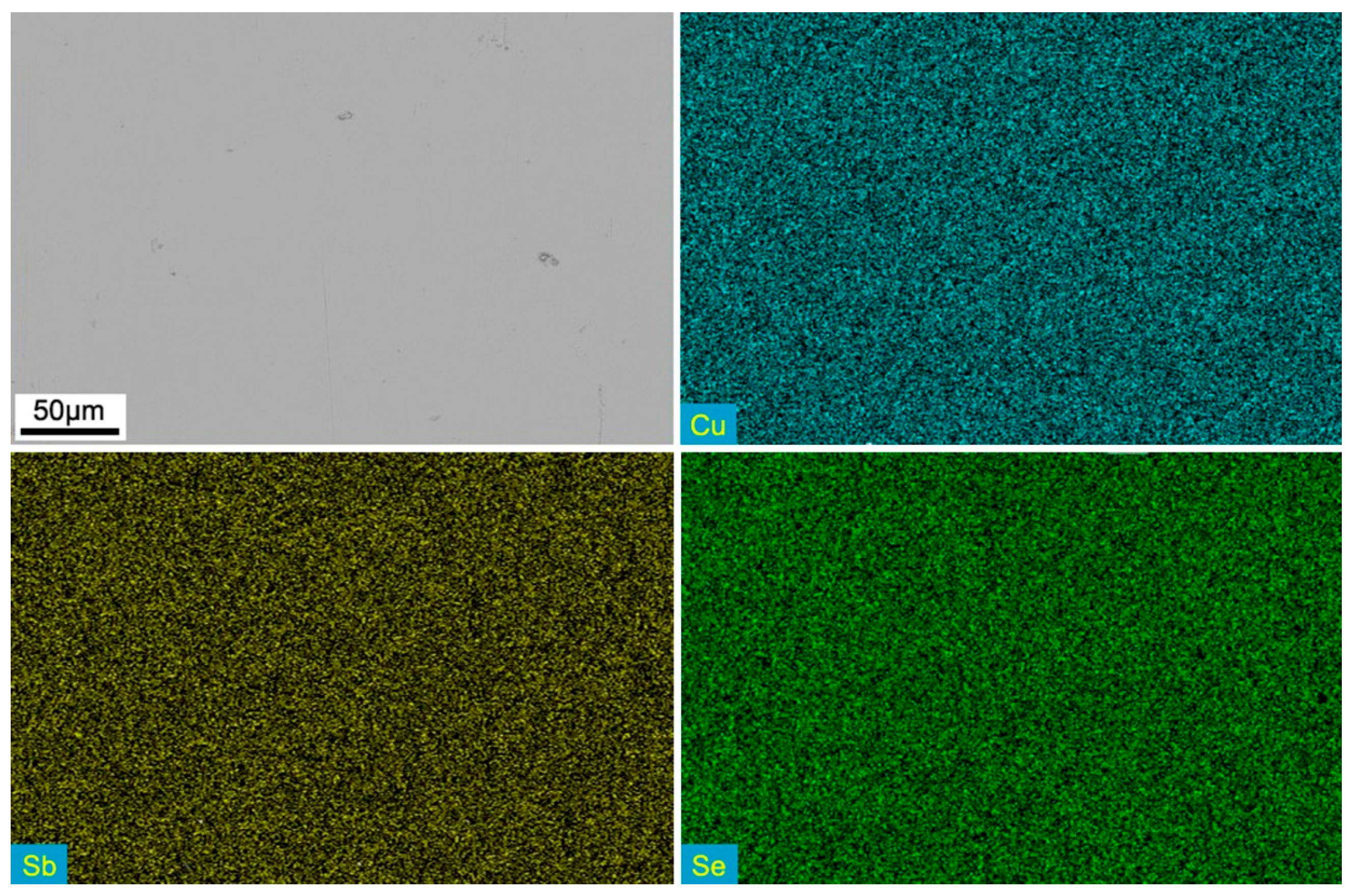
3.1. XRD Analysis and Microstructure

The X-ray diffraction patterns of Cu3Sb1−xGaxSe4 (0 ≤ x ≤ 0.015) compounds is present in Figure 1. All major XRD peaks coincide well with the stand JCPDS card of Cu3SbSe4 (No. 01-085-0003). Therefore, the Ga-doped Cu3Sb1−xGaxSe4 compounds are single phase and have the same crystallographic structure with a pure Cu3SbSe4 phase. In addition, no impurity phase was detected in the XRD results, suggesting the amount of Ga-doping in this study is within the doping limit. However, as the Ga content in Cu3Sb1−xGaxSe4 increases, no obvious peak shift is found. On the one hand, the Ga content is very low; on the other hand, it is possibly related with the similar atomic radius of Ga and Sb. Chen et al. synthesized the Cu3Sb1−xGexSe4 compounds and the small atomic radius of Ge resulted in a decrease in the lattice constant of the Cu3Sb1−xGexSe4 compounds [22]. The SEM image and elemental distribution maps, including Cu, Sb, and Se elements for the Cu3Sb0.985Ga0.015Se4 compound is displayed in Figure 2. It can be seen that each element (Cu, Sb and Se) was uniform with no notable brighter regions, indicating that all elements distributed homogeneously in the matrix. Meanwhile, no visible other phase can be found in the SEM, which is also in agreement with the XRD result above.

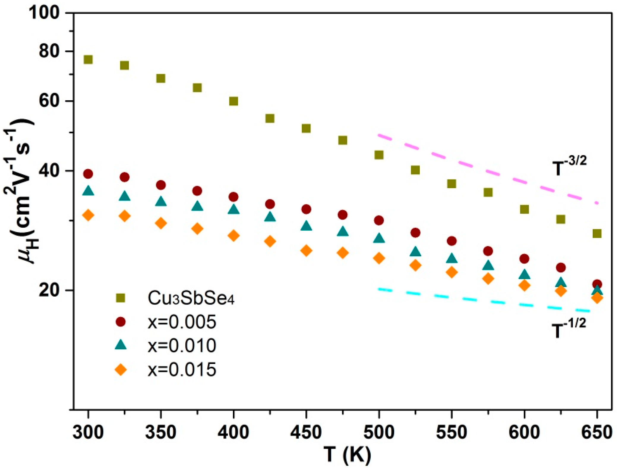
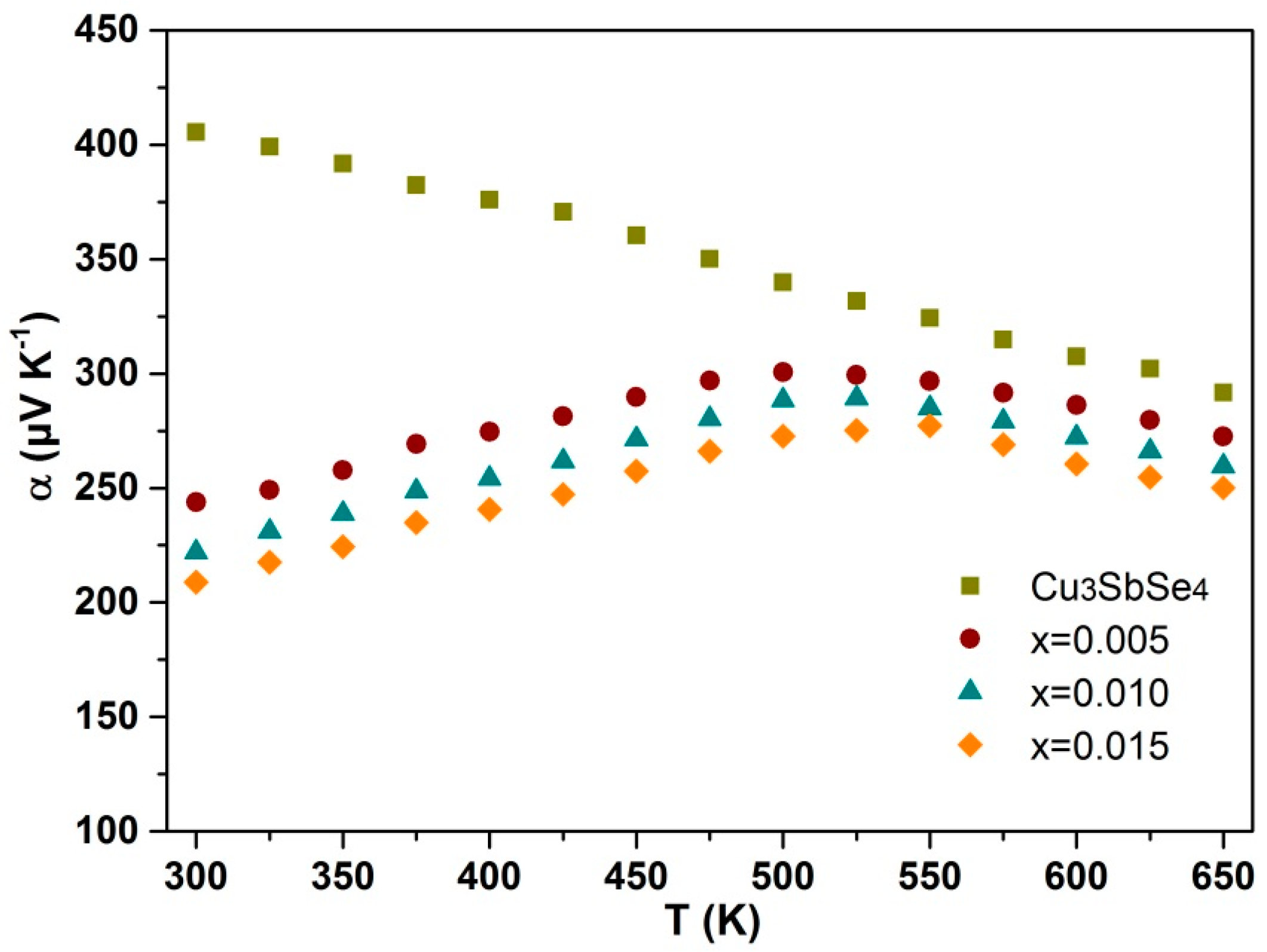
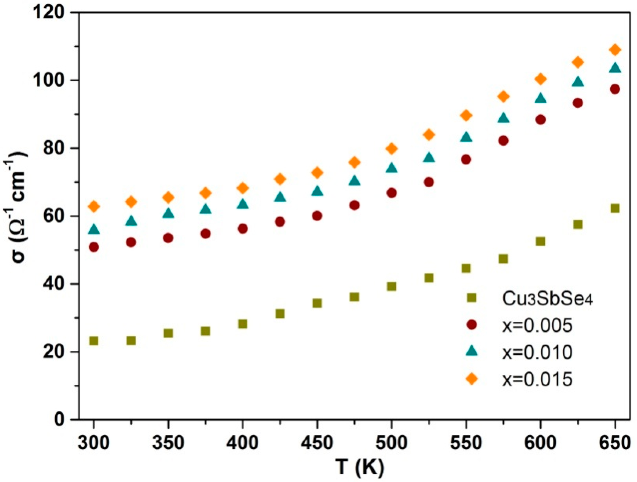
3.2. Electrical Performance

The temperature dependence of σ for the Cu3Sb1−xGaxSe4 (0 ≤ x ≤ 0.015) compounds is present in Figure 3. As the temperature increases, the σ of the Cu3Sb1−xGaxSe4 samples increases, indicating typical heavily doped semiconducting behavior. Moreover, the σ of these samples increases as the Ga content increases. The improvement in σ for Cu3Sb1−xGaxSe4 should be ascribed to an increase in carrier concentration (p) resulting from the Ga-doping. The calculated carrier concentration of pure Cu3SbSe4 was about 1.90 × 1018 cm−3. The thermoelectric properties and structural parameters of Cu3Sb1−xGaxSe4 compounds at room temperature are listed in Table 1. The hole concentration of Ga-doped Cu3Sb1−xGaxSe4 is higher than that of pure Cu3SbSe4. The hole concentration increases rapidly from 1.90 × 10¹⁸ to 12.7 × 1018 cm−3 when the Ga content increases from 0 to 0.015. Meanwhile, the corresponding μH decreases from 76.2 cm2/Vs for pure Cu3SbSe4 to 30.8 cm2/Vs for the Cu3Sb0.985Ga0.015Se4 sample. The extra ionized impurity scattering and alloy scattering should result in a decrease in μH. The μH of the Cu3Sb1−xGaxSe4 (0 ≤ x ≤ 0.015) compounds is present in Figure 4. It can be seen that the μH of these compounds shows a gradual downward trend with the increase in temperature. In addition, the relationship of μHT−3/2 can be found at high temperature, which indicates that the dominant scattering mechanism of Cu3Sb1−xGaxSe4 (0 ≤ x ≤ 0.015) compounds is phonon scattering. As the Ga content increases, the relationship of μHT−3/2 of these compounds becomes weak, indicating that the dominant mechanism is mixed scattering for the Cu3Sb1−xGaxSe4 compounds at high temperature [8]. Moreover, the μH of Ga-doped Cu3Sb1−xGaxSe4 samples in this study is between 30 and 40 cm2 V−1 s−1 at room temperature. Shi et al. calculated the μH of Cu2SnSe3 materials, and the results showed that the μH was about 52 cm2 V−1 s−1 at room temperature. The similar Hall mobility is possibly related to the similar density of states effective mass [25,26].
Figure 5 demonstrates the Seebeck coefficients for Cu3Sb1−xGaxSe4 (0 ≤ x ≤ 0.015) compounds. All of the Cu3Sb1−xGaxSe4 samples exhibit a p-type character, and the major charge carriers are holes. As the temperature increases, the α of the pure Cu3SbSe4 samples decreases, from 405 μV/K at 300 K to 291 μV/K at 650 K. Nevertheless, the α of Ga-doped samples firstly increases approximately linearly to a maximum value, and then decreases, suggesting a heavily degenerate semiconductor behavior. For example, the peak value of α for the Cu3Sb0.985Ga0.015Se4 compound is 295 μV/K at 500 K. The α decreases linearly to 260 μV/K at 650 K. Similar behaviors have been reported in In-doped Cu3SbSe4 samples [26]. In addition, the α of Ga-doped samples decreases as the Ga-doped content increases because of the increase in hole concentration. Generally, the Seebeck coefficient can be written as:
α = ± k B e [ 2 + ln 2 ( 2 π m k B T ) 3 2 h 3 p ]
where m* is the density of states effective mass, h is Planck’s constant, and kB is Boltzmann constant [4,5,6]. As the increase in hole concentration has a more significant effect than the increase in the density of states effective mass (m*, Table 1), the α of the Ga-doped Cu3Sb1−xGaxSe4 compounds decreases as Ga-doped content increases.

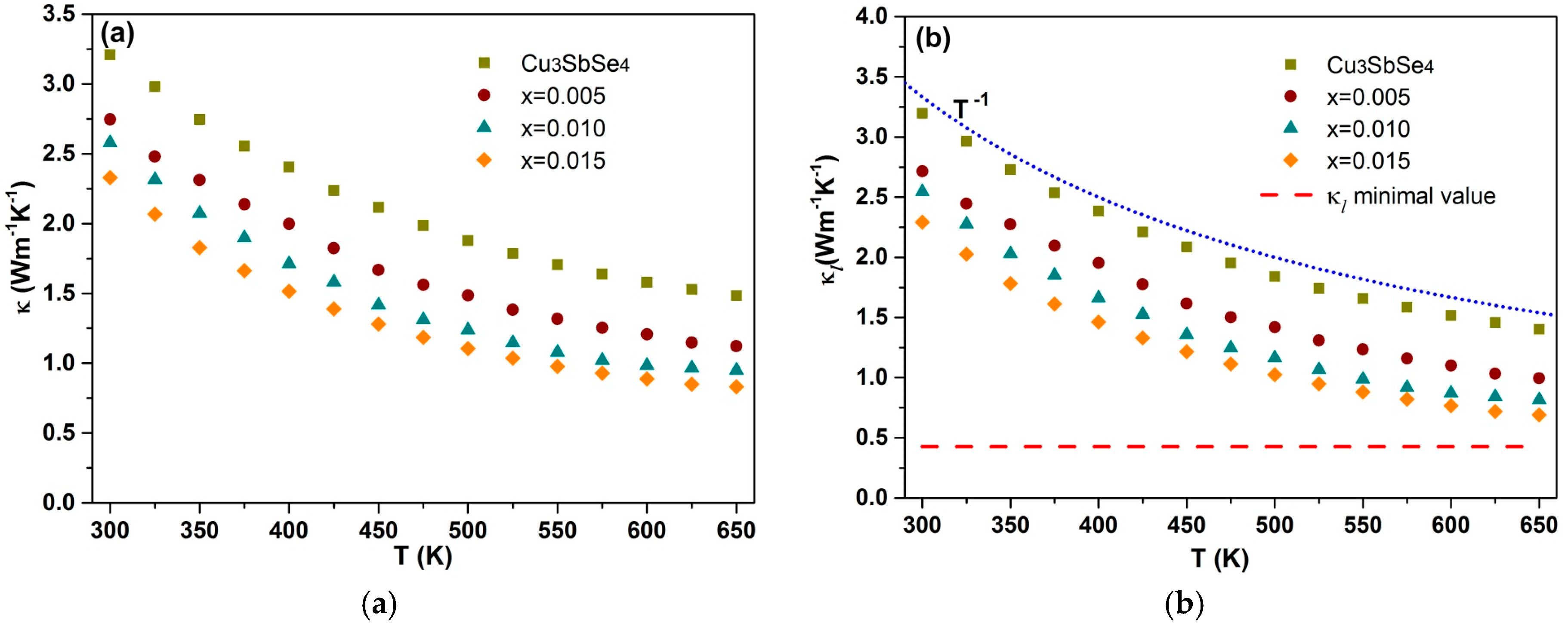
3.3. Thermal Conductivity

Figure 6a,b show the temperature dependences of the total thermal conductivity κ and the phonon part κl for Cu3Sb1−xGaxSe4 (0 ≤ x ≤ 0.015) compounds, respectively. The κ of all Cu3Sb1−xGaxSe4 compounds decreases as the temperature increases. In addition, the κ of Ga-doped Cu3Sb1−xGaxSe4 samples is markedly lower that of pure Cu3SbSe4, which should be attributed to the decrease in κl, resulting from the increase of point defect scattering. The κ of the material consists of a carrier part (κc) and a lattice part (κl). The electron part (κc) can be obtained using the Wiedemann–Franz equation, κc = L0σT, where L0 is the Lorenz number. As the Lorenz number varies with the temperature and the composition of materials, the precise Lorenz number is adopted according to the method in [27]. Therefore, the κl can be obtained by subtracting the κc from the κ. The κl of Ga-doped Cu3Sb1−xGaxSe4 compounds drastically decreases with increasing Ga content, as shown in Figure 6b. In addition, the κl shows a temperature dependence of T−1, as illustrated by the blue dotted line, indicating that phonon–phonon scattering is the dominant scattering for the pure Cu3SbSe4 sample and the Ga-doped Cu3Sb1−xGaxSe4 samples. For the Cu3Sb0.985Ga0.015Se4 sample, the κl is 2.27 W/mK at room temperature, which is reduced by 30% than that of pure Cu3SbSe4. The minimum κl of the Cu3Sb0.985Ga0.015Se4 sample in this study is 0.62 W/mK at 650K. As far as is known, the theoretical minimal value of lattice thermal conductivity, κlmin, can be evaluated according to the equation κlmin = 1/3mCv, where l, Cv, and νm are the mean free path of the phonon, the isochoric specific heat, and the mean sound velocity, respectively. The red dashed line in Figure 6b presents the theoretical minimal value of lattice thermal conductivity for pure Cu3SbSe4 and the obtained κlmin is 0.47 W m−1 K−1, as shown in the red dashed line. It also can be concluded from Figure 6b that there is still a potential possibility to further decrease the κl of the Cu3SbSe4 compound.

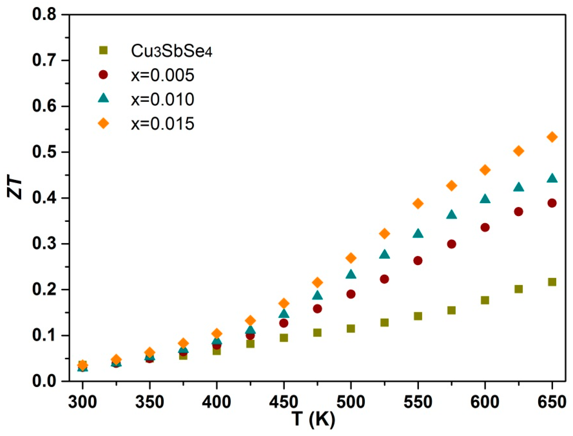
3.4. Figure of Merit

The ZT value for Cu3Sb1−xGaxSe4 (0 ≤ x ≤ 0.015) compounds is present in Figure 7. The ZT value of Cu3SbSe4 sample increases from 0.02 to 0.18 in the temperature ranged from room temperature to 650 K. Compared with the ZT value of pure Cu3SbSe4, the ZT of Ga-doped Cu3Sb1−xGaxSe4 sample is obviously improved. For example, the ZT of the Cu3Sb0.995Ga0.005Se4 compound is 0.36 at 650 K, which is one higher than the ZT of pure Cu3SbSe4. The maximal ZT value of the Cu3Sb0.985Ga0.015Se4 compound can reach 0.54 at 650 K, which is about 3 times as large as that of the pure Cu3SbSe4 compound.

4. Conclusions

In this study, p-type Ga-doped Cu3Sb1−xGaxSe4 compounds were fabricated by melting, annealing, and SPS. Compared with a pure Cu3SbSe4 compound, Ga-doped Cu3Sb1−xGaxSe4 compounds showed a large increase in electrical conductivity resulting from the substantial increase in carrier concentration. However, the Seebeck coefficient of the Cu3Sb1−xGaxSe4 compounds decreased as the Ga content increased. The Seebeck coefficient of Ga-doped samples firstly increased approximately linearly to a maximum value and then decreased. Meanwhile, the thermal conductivity of the Cu3Sb1−xGaxSe4 compounds markedly decreased because of the extra phonon scattering originating from the Ga-doping on the Sb site. Therefore, the increased electrical conductivity and the depressed lattice thermal conductivity effectively enhanced the ZT value of Cu3SbSe4. The maximum ZT value for the Cu3Sb0.985Ga0.015Se4 compounds was 0.54 at 650 K, which is around two times larger than that of pure Cu3SbSe4 compounds.

Acknowledgments

We would like to thank the help for the measurement of thermal conductivity in Tongji University, China. This work was supported by the National Natural Science Foundations of China (No. 51772132 and No. 51471076).

Author Contributions

All authors contributed to the material synthesis, measurement, data analysis, and correction of the manuscript. The design of experiment and data analysis was performed by Degang Zhao. The experiments and measurement was carried out by Di Wu and Lin Bo. The paper was written by Degang Zhao.

Conflicts of Interest

The authors declare no conflicts of interest.

References

  1. Snyder, G.J.; Toberer, E.S. Complex thermoelectric materials. Nat. Mater. 2008, 7, 105–114. [Google Scholar] [CrossRef] [PubMed]
  2. Pei, Y.Z.; Shi, X.Y.; LaLonde, A.; Wang, H.; Chen, L.D.; Snyder, G.J. Convergence of electronic bands for high performance bulk thermoelectric. Nature 2011, 473, 66–69. [Google Scholar] [CrossRef] [PubMed]
  3. Pei, Y.Z.; Wang, H.; Snyder, G.J. Band Engineering of Thermoelectric Materials. Adv. Mater. 2012, 24, 6125–6135. [Google Scholar] [CrossRef] [PubMed]
  4. Hong, M.; Chen, Z.G.; Pei, Y.Z.; Yang, L.; Zou, J. Limit of ZT enhancement in rocksalt structured chalcogenides by band convergence. Phys. Rev. B 2016, 94, 16120. [Google Scholar] [CrossRef]
  5. Hong, M.; Chen, Z.G.; Yang, L.; Zou, J. BixSb2−xTe3 nanoplates with enhanced thermoelectric performance due to sufficiently decoupled electronic transport properties and strong wide-frequency phonon scatterings. Nano Energy 2016, 20, 144–155. [Google Scholar]
  6. Fitriani, R.O.; Long, B.D.; Barma, M.C.; Riaz, M.; Sabri, M.F.; Said, S.M.; Saidur, R. A review on nanostructures of high temperature thermoelectric materials for waste heat recovery. Renew. Sustain. Energy Rev. 2016, 64, 635–659. [Google Scholar] [CrossRef]
  7. Lu, N.D.; Li, L.; Liu, M. A review of carrier thermoelectric-transport theory in organic semiconductors. Phys. Chem. Chem. Phys. 2016, 18, 19503–19525. [Google Scholar] [CrossRef] [PubMed]
  8. Hong, M.; Chasapis, T.C.; Chen, Z.G.; Yang, L.; Kanatzidis, M.G.; Snyder, G.J.; Zou, J. N-type Bi2Te3−xSex Nanoplates with enhanced thermoelectric efficiency driven by wide-frequency phonon scatterings and synergistic carrier scatterings. ACS Nano 2016, 10, 4719–4727. [Google Scholar] [CrossRef] [PubMed]
  9. Hong, M.; Chen, Z.G.; Yang, L.; Zou, J. Enhancing thermoelectric performance of Bi2Te3-based nanostructures through rational structure design. Nanoscale 2016, 8, 8681–8686. [Google Scholar] [CrossRef] [PubMed]
  10. Hong, M.; Chen, Z.G.; Yang, L.; Chasapis, T.C.; Kang, S.D.; Zou, Y.C.; Auchterlonie, G.J.; Kanatzidis, M.G.; Snyder, G.J.; Zou, J. Enhancing the thermoelectric performance of SnSe1−xTex nanoplates through band engineering. J. Mater. Chem. A 2017, 5, 10713–10721. [Google Scholar]
  11. Kosuga, A.; Plirdpring, T.; Higashine, R.; Matsuzawa, M.; Kurosaki, K.; Yamanaka, S. High temperature thermoelectric properties of Cu1−xInTe2 with a chalcopyrite structure. Appl. Phys. Lett. 2012, 100, 042108. [Google Scholar] [CrossRef]
  12. Zeier, W.G.; Pei, Y.Z.; Pomrehn, G.; Day, T.; Heinz, N.; Heinrich, C.P.; Snyder, G.J.; Tremel, W. Phonon scattering through a local anisotropic structural disorder in the thermoelectric solid solution Cu2Zn1−xFexGeSe4. J. Am. Chem. Soc. 2013, 135, 726–732. [Google Scholar] [CrossRef] [PubMed]
  13. Fan, F.J.; Yu, B.; Wang, Y.X.; Zhu, Y.L.; Liu, X.J.; Yu, S.H.; Ren, Z.F. Colloidal synthesis of Cu2CdSnSe4 nanocrystals and hot pressing to enhance the thermoelectric figure of merit. J. Am. Chem. Soc. 2011, 133, 15910–15913. [Google Scholar] [CrossRef] [PubMed]
  14. Skoug, E.J.; Cain, J.D.; Majsztrik, P.; Kirkham, M.; Morelli, D.T. Doping effects on the thermoelectric properties of Cu3SbSe4. Sci. Adv. Mater. 2011, 3, 602–606. [Google Scholar] [CrossRef]
  15. Wei, T.R.; Wang, H.; Gibbs, Z.M.; Wu, C.F.; Snyder, G.J.; Li, J.F. Thermoelectric properties of Sn-doped p-type Cu3SbSe4: A compound with large effective mass and small band gap. J. Mater. Chem. A 2014, 2, 13527–13533. [Google Scholar] [CrossRef]
  16. Yang, C.Y.; Huang, F.Q.; Wu, L.M.; Xu, K. New stannite-like p-type thermoelectric material Cu3SbSe4. J. Phys. D Appl. Phys. 2011, 44, 295404. [Google Scholar] [CrossRef]
  17. Suzumura, A.; Watanabe, M.; Nagasako, N.; Asahi, R. Improvement in thermoelectric properties of Se-free Cu3SbSe4 compound. J. Electron. Mater. 2014, 43, 2356–2360. [Google Scholar] [CrossRef]
  18. Li, X.Y.; Li, D.; Xin, H.X.; Zhang, J.; Song, C.J.; Qin, X.Y. Effects of bismuth doping on the thermoelectric properties of Cu3SbSe4 at moderate temperature. J. Alloys Compd. 2013, 561, 105–108. [Google Scholar] [CrossRef]
  19. Kumar, A.; Dhama, P.; Saini, D.S.; Banerji, P. Effects of Zn substitution at a Cu site on the transport behavior and thermoelectric properties in Cu3SbSe4. RSC Adv. 2016, 6, 5528–5534. [Google Scholar] [CrossRef]
  20. Li, D.; Li, R.; Qin, X.Y.; Song, C.J.; Xin, H.X.; Zhang, J.; Guo, G.L.; Zou, T.H.; Zhu, X.G. Co-precipitation synthesis of nanostructured Cu3SbSe4 and its Sn-doped sample with high thermoelectric performance. Dalton Trans. 2014, 43, 1888–1896. [Google Scholar] [CrossRef] [PubMed]
  21. Li, Y.Y.; Qin, X.Y.; Li, D.; Li, X.Y.; Liu, Y.F.; Zhang, J.; Song, C.J.; Xin, H.X. Transport properties and enhanced thermoelectric performance of aluminum doped Cu3SbSe4. RSC Adv. 2015, 5, 31399–31403. [Google Scholar] [CrossRef]
  22. Chang, C.H.; Chen, C.L.; Chiu, W.T.; Chen, Y.Y. Enhanced thermoelectric properties of Cu3SbSe4 by germanium doping. Mater. Lett. 2017, 186, 227–230. [Google Scholar] [CrossRef]
  23. Dan, Z.; Yang, J.Y.; Jiang, Q.H.; Fu, L.W.; Xiao, Y.; Zhou, Z.W. Improvement of thermoelectric properties of Cu3SbSe4 compound by In doping. Mater. Des. 2016, 98, 150–154. [Google Scholar]
  24. Zhang, J.; Qin, X.Y.; Li, D.; Xin, H.X.; Song, C.J.; Li, L.L.; Zhu, X.G.; Wang, Z.M.; Wang, L. Enhanced thermoelectric performance of CuGaTe2 based composites incorporated with nanophase Cu2Se. J. Mater. Chem. A 2014, 2, 2891–2985. [Google Scholar] [CrossRef]
  25. Zhao, D.G.; Ning, J.A.; Wu, D.; Zuo, M. Enhanced thermoelectric performance of Cu2SnSe3 based composites incorporated with nano-fullerene. Materials 2016, 9, 629. [Google Scholar] [CrossRef] [PubMed]
  26. Shi, X.Y.; Huang, F.Q.; Liu, M.L.; Chen, L.D. Thermoelectric properties of tetrahedrally bonded wide gap stannite compounds Cu2ZnSn1−xInxSe4. J. Am. Chem. Soc. 2009, 94, 122103. [Google Scholar] [CrossRef]
  27. Kim, H.S.; Gibbs, Z.M.; Tang, Y.L.; Wang, H.; Snyder, G.J. Characterization of Lorenz number with Seebeck coefficient measurement. APL Mater. 2015, 3, 041506. [Google Scholar] [CrossRef]
Figure 1. XRD patterns of Ga-doped Cu3Sb1−xGaxSe4 (0 ≤ x ≤ 0.015) compounds.
Energies 10 01524 g001
Figure 2. SEM image and elemental distribution maps of Cu3Sb0.985Ga0.015Se4 compounds.
Energies 10 01524 g002
Figure 3. Electrical conductivity of Cu3Sb1−xGaxSe4 (0 ≤ x ≤ 0.015) compounds.
Energies 10 01524 g003
Figure 4. Carrier mobility of Cu3Sb1−xGaxSe4 (0 ≤ x ≤ 0.015) compounds.
Energies 10 01524 g004
Figure 5. Seebeck coefficient of Cu3Sb1−xGaxSe4 (0 ≤ x ≤ 0.015) compounds.
Energies 10 01524 g005
Figure 6. (a) Total thermal conductivity (κ) and (b) lattice thermal conductivity (κl) for Cu3Sb1−xGaxSe4 (0 ≤ x ≤ 0.015) compounds. The blue dotted line represents the κl-T−1. Red dashed line shows the theoretical minimal value of lattice thermal conductivity for pure Cu3SbSe4.
Energies 10 01524 g006
Figure 7. Thermoelectric dimensionless figure of merit (ZT) for Cu3Sb1−xGaxSe4 (0 ≤ x ≤ 0.015) compounds.
Energies 10 01524 g007
Table 1. Thermoelectric properties and structural parameter of Ga-doped Cu3Sb1−xGaxSe4 (0 ≤ x ≤ 0.015) compounds at room temperature.
xκL (W m−1 K−1)Relative Densityα (μV/K)σ−1 cm−1)p (1018 cm−3)μH (cm2/Vs)m* (m0)
03.1998.5%40523.21.9076.21.2
0.0052.7198.7%24450.88.0139.21.4
0.0102.5498.3%22255.99.8435.51.6
0.0152.2998.8%20862.712.730.81.5

