Article

Simplified Route for Deposition of Binary and Ternary Bismuth Sulphide Thin Films for Solar Cell Applications

1
Department of Chemistry, Abbottabad University of Science and Technology (AUST), Abbottabad 22500, Pakistan
2
Department of Chemistry, COMSATS University Islamabad (CUI), Abbottabad 22060, Pakistan
3
Department of Chemistry, School of Natural Sciences (SNS), National University of Science and Technology (NUST), H-12, Islamabad 46000, Pakistan
4
Department of Pharmaceutical Sciences, College of Pharmacy, AlMaarefa University, Riyadh 13713, Saudi Arabia
5
Chemistry Department, Faculty of Science, King Khalid University, P.O. Box 9004, Abha 61413, Saudi Arabia
6
Biology Department, Faculty of Science, King Khalid University, P.O. Box 9004, Abha 61413, Saudi Arabia
7
Department of Semi Pilot Plant, Nuclear Materials Authority, El Maadi, P.O. Box 530, Cairo 11381, Egypt
*
Authors to whom correspondence should be addressed.
Sustainability 2022, 14(8), 4603; https://doi.org/10.3390/su14084603
Submission received: 20 February 2022 / Revised: 14 March 2022 / Accepted: 17 March 2022 / Published: 12 April 2022
(This article belongs to the Special Issue Sustainable Development of Energy Conversion and Storage Devices)

Abstract

:
For photovoltaic applications, undoped and Ni2+ doped Bi2S3 thin films were chemically deposited onto glass substrates at room temperature. Elemental diffraction analysis confirmed the successful Ni2+ incorporation in the range of 1.0 to 2.0 at. %, while X-ray Diffraction analysis revealed that orthorhombic crystal lattice of Bi2S3 was conserved while transferring from binary to ternary phase. Scanning electron microscopy images reported homogeneous and crack-free morphology of the obtained films. Optoelectronic analysis revealed that the bandgap value was shifted from 1.7 to 1.1 eV. Ni2+ incorporation also improved the carrier concentration, leading to higher electrical conductivity. Resultant optoelectronic behavior of ternary Bi2−x NixS3 thin films suggests that doping is proved to be an effectual tool to optimize the photovoltaic response of Bi2S3 for solar cell applications.

1. Introduction

The recent boom in population along with environmental and geophysical issues are forcing to switch from fossil fuels to green and sustainable energy resources [1,2,3]. To cope with this demand, there is a need to search and design new materials for renewable technologies [4,5,6]. Doping emerged as a powerful tool in the quest of designing new materials, especially for photovoltaic applications. As it can assist in improving the optoelectronic behavior by manipulating the characteristic properties of the parent material [7,8,9]. Due to its high incoming photon to electron conversion efficiency, bismuth sulphide (Bi2S3) thin films are gaining a lot of interest as a component of solar cells. The superior absorption coefficient (α > 105 cm−1) in the visible region [10] n-type electrical conductivity [11] and good structural and chemical stability [12]. According to Beer lambert’s law, Bi2S3 thin films with 200 nm thickness can absorb 95% of incident radiation. They have a direct optical band gap of 1.2–2.0 eV [10] depending on the method of sample preparation and crystal quality [13]. But its high resistance of Bi2S3 thin films can be reduced by increasing the carrier mobility with the help of doping.
The dopant, introduced as an impurity is taken as an effectual means of varying the physical and chemical properties [14,15,16,17,18]. For instance, the optical band gap of amorphous GeS films doped with bismuth is reduced, as a result of the structural disorder [19]. Antimony doped CdSe polycrystalline thin films showed good optoelectronic performance as compared to undoped ones [20]. Similarly, Sb2S3 thin films doped with 1% Sn for solar applications are reported [21]. In situ Hg2+ has been successfully introduced into the crystal lattice of PbS by doping through the chemical bath deposition practice and resulted in varied structural, optical and morphological changes [22]. The concentration of dopant is important as the properties of the resultant materials are dictated by the concentration of dopant [23]. Upon doping, impurity states are created which appear within a bandgap or outside of it as antimony doped CdSe band gap was found to decrease from 1.79 to 1.61 eV up to 0.1 mole% concentrations and was increased with further increase in the concentration of dopant [20].
Finding appropriate dopant(s) and optimization of dopant concentration is important to define, in order to alter the properties of a material appreciably. Current research work is aimed to investigate the potential of bismuth sulphide Bi2S3 thin films to be employed as an n-type nanomaterial for efficient solar harvesting. Structural, morphological, and optoelectronic properties of Bi2S3thin films will be tried to enhance by doping of earth-abundant bivalent cation i.e., Ni2+. The objective of this manuscript is threefold: viz: (a) to deposit the films of Ni-doped Bi2S3 by chemical bath deposition technique (b) to predict the mechanism of Ni-doped Bi2S3 thin films deposition, and (c) to study the optical, structural and electrical features of the deposited films.

2. Methodology

Thioacetamide (CH3CSNH2, Aldrich, 99%), bismuth nitrate (Bi(NO3)3.5H2O, BDH, 98%), ethylene diamine tetraacetic acid (C10H16N2O8, Sigma-Aldrich Chemie Gmbh, Taufkirchen, Germany, 99%), and nickel nitrate (Ni(NO3)3.6H2O, BDH, 98%) were employed as obtained for thin films construction. The substrates were commercially available microscopic glass slides (2.5 × 7.5 cm2) that had been thoroughly cleaned. Hot H2O, ethanol, chromic acid, and double distilled water were used in the cleaning process. The slides were then vacuum dried at 100 °C for 1 h. Different molar solutions of penta hydrated bismuth nitrate and hexa hydrated nickel nitrate in an acidic media were used to create the solution bath. Equimolar thioacetamide and ethylenediaminetetraacetic acid (EDTA) aqueous solutions were added in equal ratios in the above solution. In order to deposit pure and nickel doped samples in the range of 1–2 at. % Ni, six baths were prepared with varying concentrations of bismuth nitrate and nickel nitrate to deposit films and films were labeled as 0 at. % Ni, 1.0 at. % Ni, 1.25 at. % Ni, 1.50 at. % Ni, 1.75 at. % Ni, and 2.0 at. % Ni. A deionized water solution was used to react Ni2+ and Bi3+ ions with S2− ions. Five minutes were spent stirring the resulting combinations of liquids in baths. The beaker was used to dip glass films vertically. It took six hours to produce specular, uniform dark brown layers.

3. Material Characterizations

The crystallinity and phase composition of thin films were examined using an X-ray diffractometer from PANalytical Xpert’ Pro (Malvern Panalytical B.V., Almelo, Netherlands) with Cu K irradiation (k = 1.54060). Perkin Elmer Lambda 25 spectrophotometer was used to capture UV-vis spectra. The JEOL model JSM-6360A SEM was used for the scanning electron microscopic examinations and elemental analyses. The morphology is characterized by an AFM (atom force microscope) nanoscope digital equipment with a silicon nitride cantilever in contact mode. Hall effect experiments were examined using a nano-chip reliability grade hall effect device. To validate the optical properties of thin films, the ellipsometry method (sensor) was used.

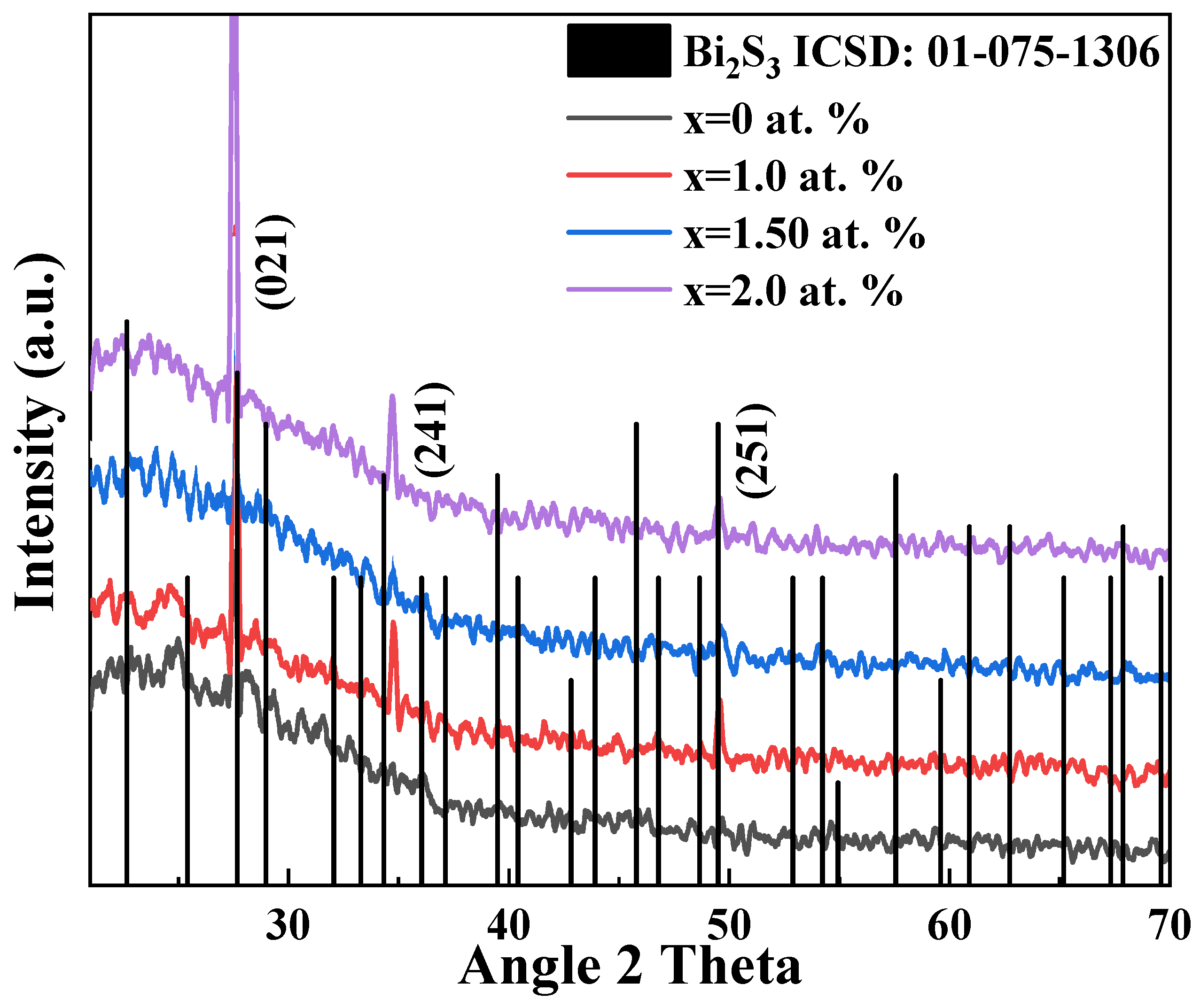
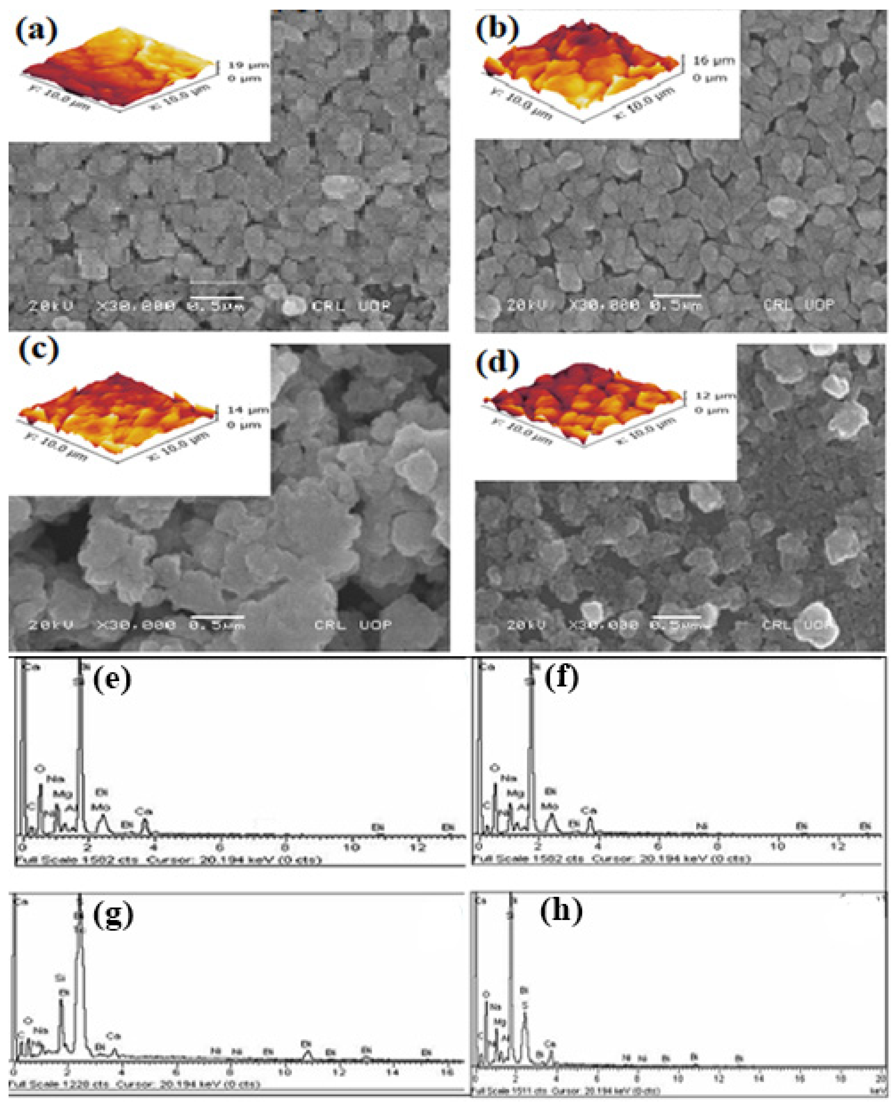
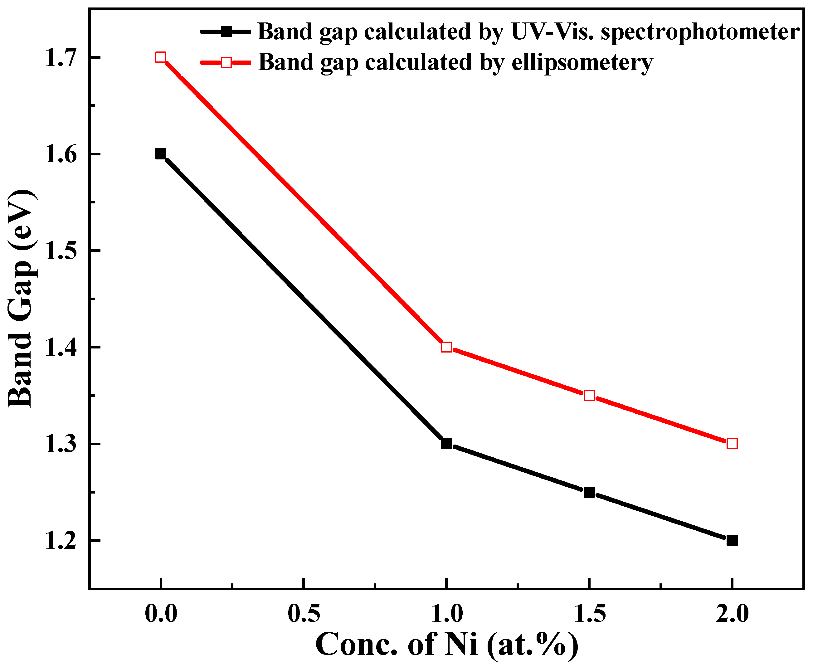
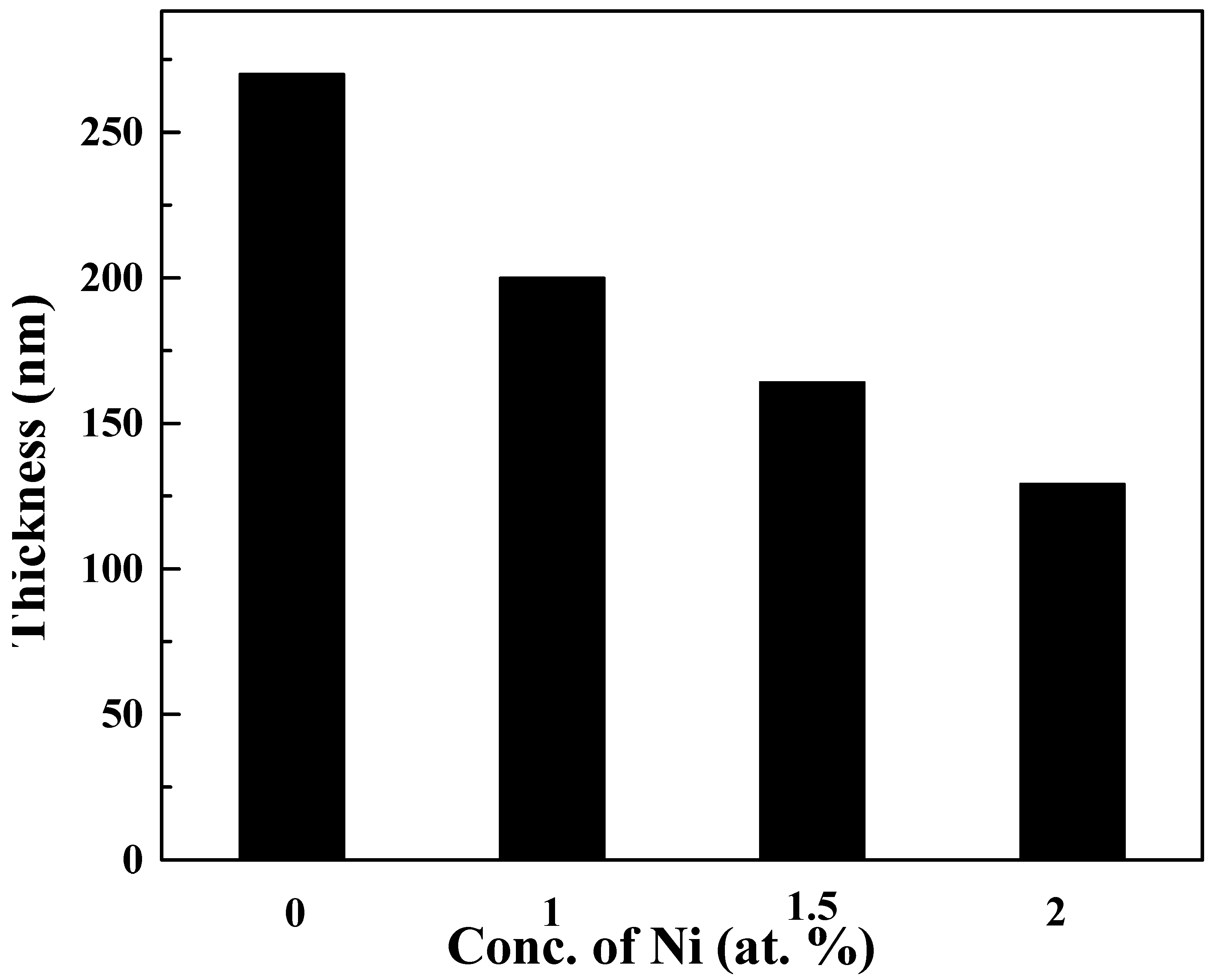
4. Results and Discussion

A number of stages occurred in a bath, including first achieving equilibrium between the complexing agent and the solvent, then forming the metal-ligand complex. The rate-determining step during Bi2S3 and Ni-doped Bi2S3 formation are attributed to the decomposition of the complex between metal precursors i.e., bismuth as well as nickel and complexing agent (EDTA). A complexing agent controls the over-growth of particles. It’s a time-consuming procedure that allows crystallites to be properly oriented and grain structure to be enhanced [24]. EDTA complexes with Bi and other metals have been widely documented, with high formation constants [25].
Bi ( N O 3 ) 3 × 5 H 2 O + E D T A 4 [ Bi ( E D T A ) ] - 1 + 5 H 2 O
N i ( N O 3 ) 3 × 6 H 2 O + E D T A - 4 [ N i ( E D T A ) ] - 2 + 6 H 2 O
Thioacetamide, used as sulphur precursor, in acidic medium shows abstraction reaction [26]. After the chalcogenide source is hydrolyzed, the metal complex and sulpher ions form a solid precipitate.
CH 3 CS NH 2 + H + CH 3 CS H 2 NH 2 CH 3 C = N H 2 + H 2 S
In aqueous medium, H2S releases S ion [27].
H 2 S H + + H S - K 1 = 5.7 × 10 7
H S H + + S 2 K 1 = 1.2 × 10 17
Overall reaction to form Ni-doped Bi2S3 is as follows:
[ Bi ( EDTA ) ] 2 + [ Ni ( EDTA ) ] 1 + CH 3 CS NH 2 H 2 O Bi 2 x Ni x S 3 + CH 3 CO NH 2 + 2 EDTA
Figure 1 shows the thickness of the films as determined by an ellipsometer. For the same deposition time (6 h), differences in the thickness of the films with variable Ni content suggest a change in the precipitation response. Variations in EDTA’s selectivity for one metal ion (Bi) over the other (Ni) and differences in the strength of one metal-EDTA complex over the other might be related to changes in the precipitation process and, ultimately, film thickness [28]. In the present studies, the drastic decrease in the thickness of the films from 269.99 to 159.09 nm (as shown in Figure 1) reveals that Ni addition slowed down the precipitation reaction and hence slow deposition of the Ni-doped Bi2S3 precipitates resulted for the same period of deposition time i.e., six hr.
XRD data is presented in Table 1. XRD patterns are shown in Figure 2. In XRD, interplanar spacing, known as d-spacing of a crystal is used for characterization and identification. i.e.,
n λ = 2 d s i n
where n is an integer θ is the Bragg’s angle, λ is the X-ray wavelength. Lattice parameters “a, b and c”, unit cell volume “Vcell”, Scherrer crystallite size “D” and X-ray density “ρX-ray” were calculated using the Equations (10)–(13).
1 d 2   =   h 2 a 2 + k 2 b 2 + l 2 c 2
V c e l l = a b c
D = k λ β cos θ B
ρ X - r a y = Z M V c e l l N A
where hkl are corresponding indices to each line in the pattern, d is the value of d-spacing of lines in XRD pattern, β is the full width at half maximum of intensity and is equal to 1.542 Å, Z is the number of molecules per formula unit, M is the molar mass, k the constant which is equal to 0.94, Vcell and NA have their usual meanings.
The polycrystalline nature of Bi2S3 and Bi2−xNixS3 thin films is shown by the sharp and well-defined peaks they display, with randomly oriented crystallites preferring growth along 021 planes. The measured diffracted peaks at 27.5°, 35.0°, and 49.3° correspond to planes (021), (240), and (251). Which are in excellent agreement with the orthorhombic structure Bi2S3 (ICSD No: 01-075-1306) and show that the material belongs to the bismuthinite phase of bismuth sulphide with lattice parameters a = 11.11, b = 11.25, and c = 3.97, all of which are in good accord with the standard pattern. No additional impurity peaks matching to Ni or Ni related as well as Bi related peaks suggest the formation of a single phase of Bi2S3 with high Ni homogeneity.
Defects are produced as a result of dopant inclusion, causing lattice deformation and a change in the XRD peak locations. The external entity, i.e., dopant, causes the XRD peak locations to move to either a higher or lower angle as a consequence of the resulting strain [29]. The shifting of diffracted peaks at 2θ~35.0° towards a larger angle gives a clear indication of the incorporation of Ni into Bi2S3 lattice [30]. The grain sizes of the films were computed using the Scherrer formula and found to be smaller when Ni ions were added, as shown in Table 1; probably due to Ni incorporation more number of nucleation centers and cites create resulting consequent reduction in grain size occurs [31].
The surface morphologies of undoped Bi2S3 and Ni-doped thin films deposited are shown in Figure 3. A noticeable difference was observed between the morphological behavior of the films with the addition of Ni from 0–2 at. %. Figure 3a i.e., 0 at. % Ni reveals the morphology of undoped samples having a compact, homogeneous and interconnected particles. Figure 3b illustrates the surface morphology of the sample containing 1 at. percent Ni, which indicates the production of discrete and well-separated agglomerations of particles with tiny particle sizes as compared to pure Bi2S3, while the texture of the particles was not changed. Furthermore, in Figure 3c, an increase in dopant, i.e., 1.5 at. percent Ni, reveals that a sample with 1.5 at. percent Ni contains irregularly shaped particles with a wide range of sizes. The increase in dopant ratio from 0 to 2 at. percent Ni seems to reduce particle size in general. Particles were discovered to grow at the cost of previously deposited particles, resulting in agglomeration as a result of tiny grain overgrowth on previously deposited particles with uneven boundaries. Higher dopant concentration films formed on the substrate were found to be loosely organised. The morphologies of the deposited samples at various dopant concentrations are connected to the compositions of the samples, which are determined by the nickel to bismuth ratio.
Three-dimensional AFM micrographs reveal morphology with little hillocks and a narrow tip, which are widely dispersed small clusters. The particles have distinct borders, and the particle size, roughness, and structure height decrease as the dopant ratio rises. A drop in film thickness may be ascribed to a decrease in film roughness with increased Ni content. The dopant concentration was increased from 1% to 2% Ni. Figure 4 illustrates the spectrum absorbance and transmittance of undoped, and doped bismuth sulphide film samples generated at room temperature.
For doped and undoped materials, the fluctuation of absorbance (A) and % transmittance was investigated in the 300–1000 nm region. The doped thin films’ strong absorbance in the 400–900 nm range, as illustrated in Figure 4a, suggests that they might be used as absorber layers in solar cells [28]. Figure 4b shows that binary bismuth sulphide thin film exhibited high transmittance i.e., more than 80%, although high transmittance values for thin-film reflect good surface homogeneity [32] which was reduced down to 40% upon doping. Figure 4c,d depicts the % age reflectance and reflection respectively.
The bandgap is the energy required to transfer an electron from the valance band into the conduction band and is usually affected by the number of factors i.e., deposition method, degree of crystallinity or amorphous of the deposited films and ratios of constituents i.e., Bi, Ni and S in doped and undoped Bi2S3 thin films [33]. The bandgaps of the constructed films were estimated by two techniques i.e., from k-spectra of the ellipsometry and by Tauc equation using the following relations respectively:
α = 4 π k λ
( α h ν ) n = A ( h ν E g )
where α: absorption coefficient
ν: frequency
h: Planks constant
Eg: bandgap
A: proportionality constant.
Figure 5 depicts direct authorised transitions in the present investigation (n:2). The films’ band gaps were estimated using UV-vis spectroscopy and ranged from 1.7 to 1.2 eV using ellipsometry. Due to the nature of the methodologies, which maintain sensitivity to distinct ranges of absorption coefficients, the bandgap values predicted by both processes differed somewhat [34] but they are in excellent agreement with the literature values which vary from 1.1 to 1.8 [35,36]. There is an inverse connection between grain sizes and optical band gap values, which corresponds to the quantum confinement effect. The band structure is exhibited and declines in bandgap values are detected owing to the participation of discrete impurity levels, since bandgap is also reliant on the composition of thin films, which differs between samples [37]. Among other factors, the crystallinity of thin films is also responsible for alteration in bandgap values [38].
The refractive index (n) and extinction coefficient (k) effect the dielectric constant (ε)
ε = (nik)
Electrical conductivity (σe) is determined from the values of wavelength (λ), refractive index (n) and speed of light (c = 2.8 × 10⁸ m/s). Mathematically, it can be calculated by Equation (15).
σe (Ω cm−1) = 2π/λnc
Thermal conductivity (σt) is determined by Equation (16).
σt (W/mk) = LT σe
L is Lorentz number, 2.45 × 10⁻⁸ W ΩK−2 and T is temperature.
Optical conductivity is calculated by mathematical Equation (17).
σo (s−1) = αnc/4π
Table 2 compares the results determined by UV-Vis. spectroscopy and ellipsometric spectroscopy with the influence of Ni content on refractive index and extinction coefficient. Using UV-vis spectroscopy data, the values of the refractive index and extinction coefficient were estimated using formulae.
Table 2 shows the values absorption coefficient, dielectric constants, electrical, optical, and thermal conductivity from optical characteristics. In metals, optical conductivity (σo) and extinction coefficient (k) values are high [39] so that reflectance approaches unity [40] while, in semiconductors, both values are reduced and hence reflectance is also reduced thereby giving higher transparency than in metals.
Figure 6 relates the comparison and behavior of refractive index (n) and extinction coefficient (k), (calculated by UV-Vis. spectroscopy and spectroscopic ellipsometry). Refractive index (n) was found to be increased with the increase in Ni content from 1.4 to 3.0 calculated from UV-Vis. spectroscopy, and in the case of ellipsometry from 1.2 to 1.8. Extinction coefficient (k) showed inverse behavior i.e., values were decreased from 1.05 to 0.75, calculated from absorbance data and 0. 9 to 0.3 for data obtained from ellipsometry. On the basis of these findings, it is clear that with increasing the Ni content, low extinction coefficient (k) and high refractive index (n) enhance the capability of these films as absorber materials in solar cells.
An area of one square centimeter was subjected for Hall studies. In the present study, all the films are n-type. Mobility values reported for the pure films are 47.7 cm2/Vs are higher than the reported value i.e., 28 cm2/Vs [41]. With the addition of Ni content in the matrix, values of carrier concentration are being increased which ultimately lead to decrease in the mobility values as reported in Table 3. Here there is a need to relate the effect of these studies with another important parameter i.e., variation in thickness of each sample, upon changes in dopant concentration. Owing to the dependence of all optoelectronic, structural and morphological properties on the thickness of thin films, comparative analysis at constant thickness by optimizing time for samples with different dopant content would be more valuable to identify the other possible areas of applications.

5. Conclusions

In brief, nickel-doped bismuth sulphide thin films having good lateral homogeneity, with energy bandgap between 1.1 and 1.7 eV and grain size having 27 to 144 nm have been successfully deposited in acidic medium via chemical bath deposition technique. Structural changes are found to have a significant effect on the performance of the material and possible area of application of the films is also highlighted based on the electrical, optical and solid-state features of the film. The optical characteristics of the films are modified by dopant incorporation by modifying the lattice parameters and thickness of the films, as shown by the correlation between the optical band gap and lattice parameters. Bandgap and optical features of the films indicate that almost all the films were found to be good absorbers in the appreciated range in the UV-Vis. regions; hence, they could be effective photovoltaic absorbers. The deductions from the spectrophotometers showed that average values n ranged from 1.9 and 2.0, k ranged between 0.026 and 0.036 were observed for different Ni/Bi ratios. Top view scan and AFM observations indicate that the surfaces of the films have been affected by the Ni contributions. Based on the findings, we determined that the Ni concentration in the ternary chalcogenide affects all of the distinctive properties of the deposited films.

Author Contributions

T.F., Conception, design of the study, writing-original draft preparation; B.I., Visualization of data, reviewed the original manuscript; M.S., Conception, design of the study, acquisition of data, interpret the data; S.I., Interpret the data, performed major experimental works, writing-original draft preparation and editing; E.B.E., Reviewing data, critical revision and financial support; N.S.A., Visualization of data, EDX analysis, writing reviewing and editing; H.A.I., Conception, visualization of data, performed XRD analysis, acquisition of data. All authors have read and agreed to the published version of the manuscript.

Funding

This research received no external funding.

Institutional Review Board Statement

Not applicable.

Informed Consent Statement

Not applicable.

Data Availability Statement

The data will be available on request.

Acknowledgments

The authors extend their appreciation to the Deanship of Scientific Research at King Khalid University for supporting this work through research groups program under grant number R.G.P.2/107/42. The authors extend their appreciation to the Research Center at AlMaarefa University for funding this work under TUMA project agreement number (TUMA-2021-4).

Conflicts of Interest

There is no conflict of interest to be reported.

References

  1. Vo, D.H.; Vo, A.T. Renewable energy and population growth for sustainable development in the Southeast Asian countries. Energy Sustain. Soc. 2021, 11, 30. [Google Scholar] [CrossRef]
  2. Iqbal, S. Spatial Charge Separation and Transfer in L-Cysteine Capped NiCoP/CdS Nano-Heterojunction Activated with Intimate Covalent Bonding for High-Quantum-Yield Photocatalytic Hydrogen Evolution. Appl. Catal. B Environ. 2020, 274, 119097. [Google Scholar] [CrossRef]
  3. Irfan, R.M.; Tahir, M.H.; Nadeem, M.; Maqsood, M.; Bashir, T.; Iqbal, S. Fe3C/CdS as noble-metal-free composite photocatalyst for highly enhanced photocatalytic H2 production under visible light. Appl. Catal. A Gen. 2020, 603, 117768. [Google Scholar] [CrossRef]
  4. Muhammad Irfan, R.; Hussain Tahir, M.; Maqsood, M.; Lin, Y.; Bashir, T.; Iqbal, S.; Zhao, J.; Gao, L.; Haroon, M. CoSe as Non-Noble-Metal Cocatalyst Integrated with Heterojunction Photosensitizer for Inexpensive H2 Production under Visible Light. J. Catal. 2020, 390, 196–205. [Google Scholar] [CrossRef]
  5. Hussain, W.; Malik, H.; Hussain, R.A.; Hussain, H.; Green, I.R.; Marwat, S.; Bahadur, A.; Iqbal, S.; Farooq, M.U.; Li, H.; et al. Synthesis of MnS from Single- and Multi-Source Precursors for Photocatalytic and Battery Applications. J. Electron. Mater. 2019, 48, 2278–2288. [Google Scholar] [CrossRef]
  6. Iqbal, S.; Bahadur, A.; Saeed, A.; Zhou, K.; Shoaib, M.; Waqas, M. Electrochemical performance of 2D polyaniline anchored CuS/Graphene nano-active composite as anode material for lithium-ion battery. J. Colloid Interface Sci. 2017, 502, 16–23. [Google Scholar] [CrossRef]
  7. Sathiya Priya, A.; Geetha, D.; Henry, J. Effect of Cu and Sm doping on the ferroelectric character of bismuth ferrite thin films. Phosphorus Sulfur Silicon Relat. Elem. 2021, 197, 158–163. [Google Scholar] [CrossRef]
  8. Iqbal, S.; Bahadur, A.; Anwer, S.; Ali, S.; Irfan, R.M.; Li, H.; Shoaib, M.; Raheel, M.; Anjum, T.A.; Zulqarnain, M. Effect of temperature and reaction time on the morphology of l-cysteine surface capped chalcocite (Cu2S) snowflakes dendrites nanoleaves and photodegradation study of methyl orange dye under visible light. Colloids Surf. A Physicochem. Eng. Asp. 2020, 601, 124984. [Google Scholar] [CrossRef]
  9. Sher, M.; Javed, M.; Shahid, S.; Iqbal, S.; Qamar, M.A.; Bahadur, A.; Qayyum, M.A. The controlled synthesis of g-C3N4/Cd-doped ZnO nanocomposites as potential photocatalysts for the disinfection and degradation of organic pollutants under visible light irradiation. RSC Adv. 2021, 11, 2025–2039. [Google Scholar] [CrossRef]
  10. Ahire, R.; Deshpande, N.; Gudage, Y.; Sagade, A.; Chavhan, S.; Phase, D.; Sharma, R. A comparative study of the physical properties of CdS, Bi2S3 and composite CdS–Bi2S3 thin films for photosensor application. Sens. Actuators A Phys. 2007, 140, 207–214. [Google Scholar] [CrossRef]
  11. Rincón, M.; Campos, J.; Suárez, R. A comparison of the various thermal treatments of chemically deposited bismuth sulphide thin films and the effect on the structural and electrical properties. J. Phys. Chem. Solids 1999, 60, 385–392. [Google Scholar] [CrossRef]
  12. Mageshwari, K.; Sathyamoorthy, R. Nanocrystalline Bi2S3 thin films grown by thio-glycolic acid mediated successive ionic layer adsorption and reaction (SILAR) technique. Mater. Sci. Semicond. Process. 2013, 16, 43–50. [Google Scholar] [CrossRef]
  13. Ajiboye, T.O.; Onwudiwe, D.C. Bismuth sulphide based compounds: Properties, synthesis and applications. Results Chem. 2021, 3, 100151. [Google Scholar] [CrossRef]
  14. Su-juan, Z.; Ling-fang, Y.; Dan, S.; Ying-jie, W. Effect of Cs+, Ag+, Fe3+ Doping and Ag+, Fe3+ Co-Doping Contents on Photocatalytic Activity of TiO2 Films. In Proceedings of the 2011 Symposium on Photonics and Optoelectronics (SOPO), Wuhan, China, 16–18 May 2011; pp. 1–4. [Google Scholar]
  15. Chu, D.; Yuan, X.; Qin, G.; Xu, M.; Zheng, P.; Lu, J.; Zha, L. Efficient carbon-doped nanostructured TiO2 (anatase) film for photoelectrochemical solar cells. J. Nanopart. Res. 2008, 10, 357–363. [Google Scholar] [CrossRef]
  16. Iqbal, S.; Bahadur, A.; Javed, M.; Hakami, O.; Irfan, R.M.; Ahmad, Z.; AlObaid, A.; Al-Anazy, M.M.; Baghdadi, H.B.; Abd-Rabboh, H.S.M.; et al. Design Ag-doped ZnO heterostructure photocatalyst with sulfurized graphitic C3N4 showing enhanced photocatalytic activity. Mater. Sci. Eng. B 2021, 272, 115320. [Google Scholar] [CrossRef]
  17. Bahadur, A.; Iqbal, S.; Shoaib, M.; Saeed, A. Electrochemical study of specially designed graphene-Fe3O4-polyaniline nanocomposite as a high-performance anode for lithium-ion battery. Dalton Trans. 2018, 47, 15031–15037. [Google Scholar] [CrossRef]
  18. Anwer, S.; Anjum, D.H.; Luo, S.; Abbas, Y.; Li, B.; Iqbal, S.; Liao, K. 2D Ti3C2Tx MXene nanosheets coated cellulose fibers based 3D nanostructures for efficient water desalination. Chem. Eng. J. 2021, 406, 126827. [Google Scholar] [CrossRef]
  19. Romanyuk, R. Optical properties of amorphous (GeS)1−x Bix (0 ≤ x ≤ 0.15) films and a tentative cluster model for their structure. Inorg. Mater. 2014, 50, 120–123. [Google Scholar] [CrossRef]
  20. Masumdar, E.; Gaikwad, V.; Pujari, V.; More, P.; Deshmukh, L. Some studies on chemically synthesized antimony-doped CdSe thin films. Mater. Chem. Phys. 2003, 77, 669–676. [Google Scholar] [CrossRef]
  21. Ismail, B.; Mushtaq, S.; Khan, A. Enhanced grain growth in the sn doped Sb2S3 thin film absorber materials for solar cell applications. Chalcogenide Lett. 2014, 11, 37–45. [Google Scholar]
  22. Tototzintle, M.Z.; Castilla, S.R.; Luevano, R.; Hernandez, K.B.; Sotarriba, J.G.; Yañez, A.C. PbS:Hg2+ Nanostructures Films by Chemical Bath. J. Mater. Sci. Eng. A 2013, 3, 407–414. [Google Scholar]
  23. Yang, Y.; Xiong, X.; Yin, H.; Zhao, M.; Han, J. Study of copper bismuth sulphide thin films for the photovoltaic application. J. Mater. Sci. Mater. Electron. 2019, 30, 1832–1837. [Google Scholar] [CrossRef]
  24. Mane, R.S.; Sankapal, B.R.; Lokhande, C.D. Thickness dependent properties of chemically deposited As2S3 thin films from thioacetamide bath. Mater. Chem. Phys. 2000, 64, 215–221. [Google Scholar] [CrossRef]
  25. Raoot, S.; Raoot, K. Selective complexometric determination of bismuth with mercaptans as masking agents, and its estimation in alloys. Talanta 1985, 32, 1011–1012. [Google Scholar] [CrossRef]
  26. Kishore, K.; Dwibedy, P.; Dey, G.; Naik, D.; Moorthy, P. Nature of the transient species formed during pulse radiolysis of thioacetamide in aqueous solutions. Res. Chem. Intermed. 1998, 24, 35–45. [Google Scholar] [CrossRef]
  27. Mane, R.; Sankapal, B.; Lokhande, C. Studies on chemically deposited nanocrystalline Bi2S3 thin films. Mater. Res. Bull. 2000, 35, 587–601. [Google Scholar] [CrossRef]
  28. Green, M.A.; Emery, K.; Hishikawa, Y.; Warta, W.; Dunlop, E.D. Solar cell efficiency tables (Version 45). Prog. Photovolt. Res. Appl. 2015, 23, 1–9. [Google Scholar] [CrossRef]
  29. Ginting, M.; Taslima, S.; Sebayang, K.; Aryanto, D.; Sudiro, T.; Sebayang, P. Preparation and characterization of zinc oxide doped with ferrite and chromium. AIP Conf. Proc. 2017, 1862, 030062. [Google Scholar]
  30. Taziwa, R.; Meyer, E.; Katwire, D.; Ntozakhe, L. Influence of carbon modification on the morphological, structural, and optical properties of zinc oxide nanoparticles synthesized by pneumatic spray pyrolysis technique. J. Nanomater. 2017, 2017, 9095301. [Google Scholar] [CrossRef]
  31. Yilmaz, M.; Aydoğan, Ş. The effect of Pb doping on the characteristic properties of spin coated ZnO thin films: Wrinkle structures. Mater. Sci. Semicond. Process. 2015, 40, 162–170. [Google Scholar] [CrossRef]
  32. Sharma, S.; Jain, K.K.; Sharma, A. Solar Cells: In Research and Applications—A Review. Mater. Sci. Appl. 2015, 6, 1145. [Google Scholar] [CrossRef] [Green Version]
  33. Barote, M.A.Y.; Masumdar, A.A. Synthesis, characterization and photoelectrochemical properties of n-CdS thin films. Physica B 2011, 406, 1865. [Google Scholar] [CrossRef]
  34. Podraza, N.J.; Qiu, W.; Hinojosa, B.B.; Xu, H.; Motyka, M.A.; Phillpot, S.R.; Baciak, J.E.; Trolier-McKinstry, S.; Nino, J.C. Band gap and structure of single crystal BiI3: Resolving discrepancies in literature. J. Appl. Phys. 2013, 114, 033110. [Google Scholar] [CrossRef] [Green Version]
  35. Roy, C.B.; Nandi, D.K.; Mahapatra, P.K. Photoelectrochemical cells with n-type ZnSe and n-type Sb2Se3 thin film semiconductor electrodes. Electrochim. Acta 1986, 31, 1227. [Google Scholar] [CrossRef]
  36. Linhart, W.M.; Zelewski, S.J.; Scharoch, P.; Dybała, F.; Kudrawiec, R. Nesting-like band gap in bismuth sulphide Bi2S3. J. Mater. Chem. C 2021, 9, 13733–13738. [Google Scholar] [CrossRef]
  37. Hankare, P.P.; Chate, P.A.; Sathe, D.J. Zinc sulphide semiconductor electrode synthesis and the photoelectrochemical application. J. Alloys Compd. 2009, 487, 367. [Google Scholar] [CrossRef]
  38. Deshmukh, L.P.; Rotti, C.B.; Garadkar, K.M. Cd1−xZnxS thin film electrode for photoelectrochemical (PEC) applications. Mater. Chem. Phys. 1997, 50, 45. [Google Scholar] [CrossRef]
  39. Rajpure, K.Y.; Bhosale, C.H. Sb2S3 semiconductor-septum rechargeable storage cell. Mater. Chem. Phys. 2000, 64, 14. [Google Scholar] [CrossRef]
  40. Bagdare, P.B.; Patil, S.B.; Singh, A.K. Phase evolution and PEC performance of ZnxCd1−xS nanocrystalline thin films deposited by CBD. J. Alloy. Compd. 2012, 506, 120–124. [Google Scholar]
  41. MacLachlan, A.J.; O’Mahony, F.T.F.; Sudlow, A.L.; Hill, M.S.; Molloy, K.C.; Nelson, J.; Haque, S.A. Solution-Processed Mesoscopic Bi2S3:Polymer Photoactive Layers. ChemPhysChem 2014, 15, 1019–1023. [Google Scholar] [CrossRef] [PubMed] [Green Version]
Figure 1. Variation in thickness versus concentration of dopant of selected Ni-doped Bi2S3 thin films.
Sustainability 14 04603 g001
Figure 2. XRD Analysis of undoped and selected Ni-doped Bi2S3 thin films.
Sustainability 14 04603 g002
Figure 3. SEM images of undoped (a,b) and selected Ni-doped (c,d) Bi2S3 thin films and their corresponding EDX (eh) analysis.
Sustainability 14 04603 g003
Figure 4. Plot of the (a) absorbance, (b) % transmittance, (c) % reflectance and (d) reflection versus wavelength for undoped and selected Ni-doped Bi2S3 thin films.
Sustainability 14 04603 g004
Figure 5. Plot of the bandgap versus concentration of dopant for undoped and selected Ni-doped Bi2S3 thin films.
Sustainability 14 04603 g005
Figure 6. Plot of (a) refractive index (n) and (b) extinction coefficient (k) versus concentration of dopant for undoped and selected Ni-doped Bi2S3 thin films.
Sustainability 14 04603 g006
Table 1. Crystallographic parameters calculated from XRD data for undoped and selected Ni-doped Bi2S3 thin films.
Ni Content
(at. %)
Calculated Lattice ConstantsVolume of Cell (Å3)Average Crystallite Size (nm)X-ray Density
(gcm−3)
a (Å)b (Å)c (Å)
011.1111.713.524582887.46
1.011.1011.683.895092356.71
1.511.1211.224.165192116.58
2.011.6511.164.025221596.54
Standard values for the ICSD No: 01-075-1306 (a = 11.11 Å, b = 11.25 Å and c = 3.97 Å)
Table 2. Optical parameters calculated from UV-Vis. spectroscopic analysis for undoped and Ni-doped S3 thin films.
ParametersConc. of Ni (at. %)
01.01.251.51.752.0
α × 104 (cm−1)0.421.071.692.162.743.74
ε0.084.565.006.817.308.76
σe × 103 (Ω cm−1)0.3450.0100.0420.0440.0630.079
σo × 1012 (s−1)1.331.061.331.852.012.9
σt × 10−4 (Ω cm/K)0.00631.031.151.721.682.08
Table 3. Hall studies of undoped and selected Ni-doped Bi2S3 films.
Ni Conc.
(at. %)
I (µA)Resistivity
(Ω cm) × 102
Conductivity
(Ω−1 cm−1) × 102
Carrier Conc. (cm−2) × 1011Sheet Carrier Mobility
(cm2/Vs) × 102
00.12.990.393−0.0164.77
1.00.10.1885.4−2.623.14
1.50.10.2763.62−2.710.35
2.00.10.4312.32−11.80.06
Publisher’s Note: MDPI stays neutral with regard to jurisdictional claims in published maps and institutional affiliations.

