Article

A Comparative Analysis of Soft Switching Techniques in Reducing the Energy Loss and Improving the Soft Switching Range in Power Converters

1
Department of Electrical and Electronic Engineering, Green University of Bangladesh, Dhaka 1207, Bangladesh
2
Department of Electrical and Electronic Engineering, University Technology Malaysia, Johor Bahru 80542, Malaysia
3
Department of Computer Science and Engineering, Independent University, Dhaka 1229, Bangladesh
4
Electrical and Computer Engineering, National Technical University of Athens, 10682 Athens, Greece
5
Electromechanics Engineering Department, Faculty of Engineering, Heliopolis University, Cairo 11785, Egypt
*
Author to whom correspondence should be addressed.
Electronics 2022, 11(7), 1062; https://doi.org/10.3390/electronics11071062
Submission received: 31 December 2021 / Revised: 25 February 2022 / Accepted: 16 March 2022 / Published: 28 March 2022
(This article belongs to the Special Issue Power Converter Design, Control and Applications)

Abstract

:
This paper presents a comparative analysis of the zero-voltage zero-current switching (ZVZCS) soft switching technique with zero-voltage switching (ZVS) and zero-current switching (ZCS) counterparts. The generalization of the voltage–current crossover or the energy loss factor obtained from simulation of the prototype converter shows that the ZVZCS significantly reduces the losses and helps to improve the efficiency of the converter as compared to the ZVS or the ZCS. On the other hand, it is also found that the soft switching range of operation of the ZVS and the ZCS is largely affected by the maximum switch voltage and switch current, respectively. In contrast, these factors have a negligible effect on the ZVZCS operation which results in an extended range of soft switching operation. Additionally, a detailed PSPICE simulation is performed for selected ZVS, ZCS, and ZVZCS topologies from the recent literature, and the switching losses in the main switches of the converters are measured. It is observed that the energy losses in the ZVZCS mode are reduced on average by approximately 26% at turn on and 20% at turn off as compared to the ZVS and the ZCS. Furthermore, the low standard deviation in this mode confirms a stable low-loss profile which renders an extended soft switching range. An experimental test is also conducted by building the prototype converter to verify the simulation results. It is found that the switching losses are minimum while the converter is operated in the ZVZCS mode. Additionally, the efficiency drop remains consistently low as compared to the ZVS and the ZCS in the whole operating range. Accordingly, the simulation and the experimental results are both found to be consistent.

1. Introduction

DC–DC converters are widely used industrial and consumer electronic devices. With the increase in renewable energy penetration into the grid, DC–DC converters have become an integral part of the system. Hence, these converters are required to be efficient. Switching losses represent primary contributors to the efficiency reduction of DC–DC converters. This is particularly critical when the converter is operated at a low power level and high switching frequency. To alleviate this problem, various soft switching techniques have been proposed [1,2,3,4,5,6,7,8,9,10,11,12,13,14,15], which include zero-voltage switching (ZVS), zero-current switching (ZCS), and zero-voltage zero-current switching (ZVZCS). When operating in these modes, the voltage and current transients are manipulated to reduce the voltage–current crossover, otherwise defined as switching loss. In the ZVS case, the voltage transients at the turn on and turn off instants are restricted to reduce large crossover with the current. On the other hand, for the ZCS, the current transients, rather than the voltage, are controlled in order to achieve the same goal. In ZVZCS [16,17,18,19,20,21,22], both voltage and current transients are simultaneously controlled to reduce the crossover at both turn on and turn off instants. This results in a significant improvement in switching losses and, hence, higher efficiency. In particular, this is a direct consequence of simultaneous manipulation of both the voltage and the current transients to reduce the crossover losses. However, the existing studies [16,17,18,19,20,21,22] did not explicitly cover this issue or analyze the ZVZCS from this point of view. Hence, considering these factors, it is worth investigating the standing of ZVZCS relative to the other soft switching techniques (i.e., ZVS and ZCS) in terms of loss reduction capability and soft switching range of operation. Eventually, a generic conclusion regarding the superiority or inferiority of the ZVZCS technique to the ZVS and the ZCS can be reached. Additionally, this would further enhance the understanding of soft switching techniques and their implementation into DC–DC converters.
Considering this literature gap, this paper presents a generalized analysis to investigate the relative status of the ZVZCS compared to the ZVS and the ZCS techniques. For this purpose, the switching transients of the ZVS, ZCS, and ZVZCS are linearized from the simulation results of a prototype converter. A geometrical analysis to determine the crossover energy and the soft switching range of operation is then performed, as demonstrated in Section 2 and Section 3. It is found that the crossover energy is reduced in the ZVZCS as compared to the ZVS and the ZCS. In addition, the dependency of the soft switching performance on the input voltage and the switch current is lowered. Next, a simulation for comparative analysis is performed. A large number of converters are selected (to retain a large sample size) for simulation, and the results are presented in Section 4. The experimental analysis is then performed by building a prototype converter which is independently operable in different soft switching modes (i.e., ZVS, ZCS, and ZVZCS). The experimental results are demonstrated in Section 5. It is found that the ZVZCS further reduces the loss margin to improve the efficiency and extends the soft switching range by lowering the dependency on the switch voltage and current. Consequently, the superiority of the ZVZCS to the other soft switching techniques in terms of energy loss reduction capability and an extension of the soft switching range of operation is proven. Lastly, Section 6 draws the conclusions.

2. Analysis of the Soft Switching Modes for Energy Loss Measurement

The soft switching modes are analyzed to find the gross voltage–current crossover area induced at the turn on instant for each mode and the respective improvement from the hard switching counterpart by simulating the prototype ZVZCS converter [22] shown in Figure 1. Only the turn on instant is selected for the analysis as the turn off situation can be replicated by replacing simple parameters. To perform the theoretical analysis, the following assumptions are made: (1) all the voltage and current transients are considered linearized; (2) the converter operates in the CCM mode; (3) the standard ZVS and ZCS conditions are assumed where the switch voltage and the switch current remain always positive. The specifications are given in Table 1. The PWM switching is described in Section 5. It is to be mentioned that the switching transients are typical for a MOSFET. An identical analysis can be performed for an IGBT. In this case, the energy loss would be higher at the turn off because of the tail current. Aside from this, the comparative results will be identical as long as the comparison is made on the basis of energy loss (or the crossover area).

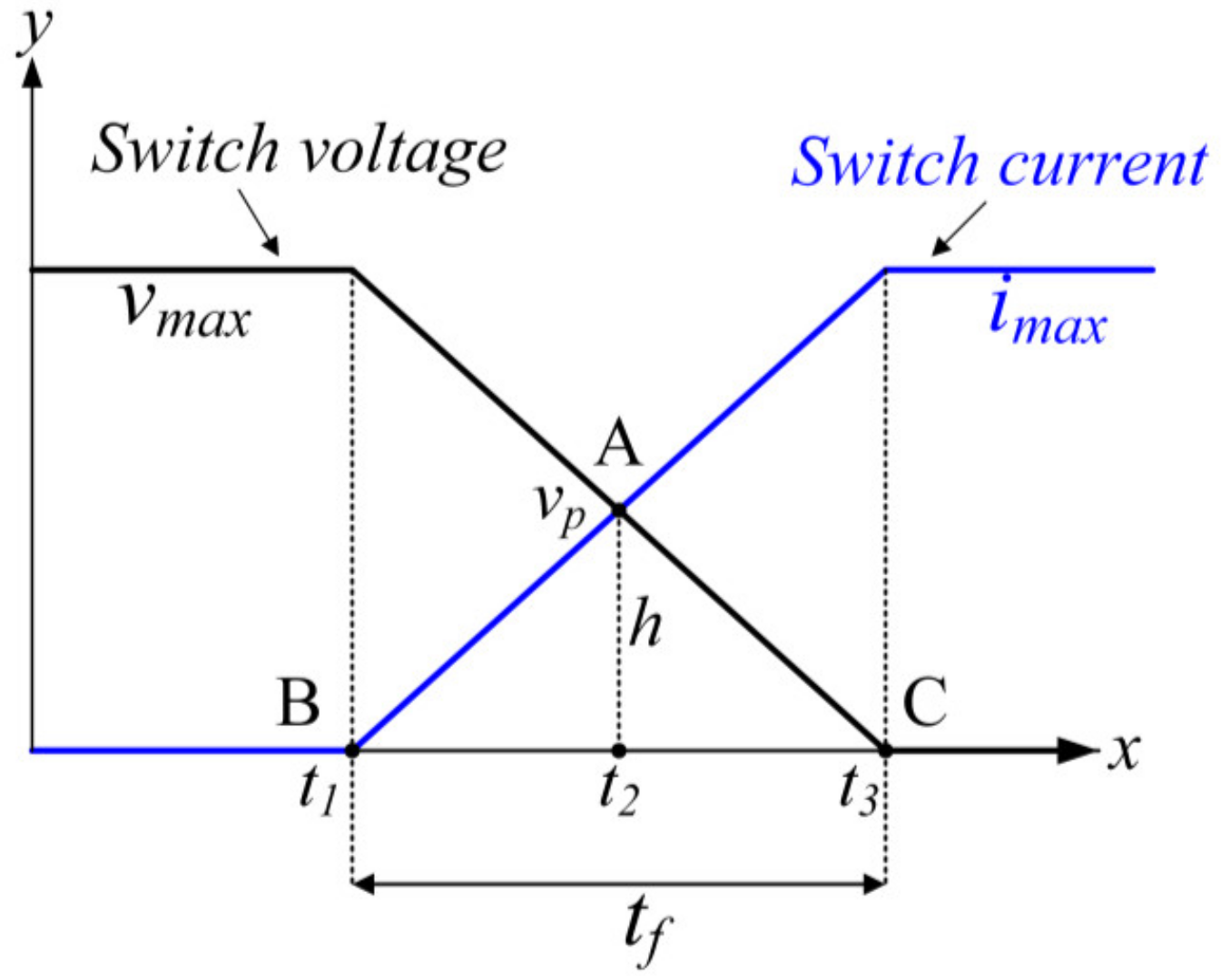
2.1. The Hard Switching Mode

The crossover area that is formed due to the voltage and current rise and fall times (at the switch turn on instant) is shown in Figure 2. In Figure 3, the switching waveform pattern for PSPICE simulation is shown to justify the approximation in Figure 2 for the theoretical analysis. Hence, the crossover area can be approximated by the area of the triangle Δ ABC.
A r e a   of   Δ ABC = 0.5 t 3 t 1 h ,
where (t3t1) is the base, and h is the height of the triangle, respectively. Consequently, for switching frequency fs, the total energy loss at the turn on instant is
E H S , t n l o s s = 0.5 t 3 t 1 h f s .
It can be assumed that the fall time of the switch voltage (tf) and the rise time of the switch current (tr) are equal. Hence, Equation (2) can be rewritten as
E H S , t o n l o s s = ( 0.5 ) ( t f ) ( h ) ( f s ) .
Now, the switch voltage v can be described as
v v max v max = t t 1 t f ,
where t1 < t < t3.
The voltage and the current transients intersect at A located at t2 on the x-axis. Hence, the voltage v at t2 can be obtained by replacing t = t2 in Equation (4).
v p = ( t 2 t 1 t f ) ( v max ) + v max ,
where vmax is the maximum voltage applied across the switch. Hence, by replicating the concept in Equation (2), the total energy loss at turn on becomes
E H S , t o n l o s s = ( 0.5 ) t 3 t 1 t 2 t 1 t f v max + v max ( f s ) .
Now, from Figure 2, it is obvious that t2t1 = (0.5)(t3t1) = 0.5 tf.
Hence,
E H S , t o n l o s s = 0.25 t f v max ( f s ) = 0.5 v max 0.5 t f ( f s )
where fs is the switching frequency. Similarly, at turn off, the energy loss is
E H S , t o f f l o s s = 0.5 v max 0.5 t r ( f s ) ,
where tr is the voltage rise time.
By replacing the parameter values from Figure 3, the energy loss amounts to
E H S , t o f f l o s s = 0.5 × 50 0.5 × 10 6 100 × 10 3 = 12.5   W .

2.2. The Zero-Voltage Switching Mode (ZVS)

In this mode, the sharp voltage fall at turn on is restricted by emulating zero voltage across the switch. This is achieved by turning on the body diode of the switch and discharging the passive snubber element. For computation purpose, it is assumed that the voltage transient is linear. The original hard switching curve for v is shown by the broken line. Hence, as obvious from Figure 4 and justifiable through Figure 5, the fall time for v is reduced and the voltage–current intersection is shifted left to a new position D from the hard switching point at A. The new intersection point D is located between t2 and t1 and considered at t 2 . Consequently, the switch voltage v can be expressed as
v v max v max = t t 1 t 2 t 1 = t t 1 t f , ZVS ,
where t1 < t < t 3 .
If voltage is v p at t 2 , then, from Equation (9), it can be obtained as
v p = t 2 t 1 t 3 t 1 v m a x max
Consequently, the energy loss in the ZVS turn on can be derived from Equation (1) as
E ZVS , t o n l o s s = 0.5 t 3 t 1 t 2 t 1 t 3 t 1 v max + v max ( f s ) = 0.5 t f , ZVS t 2 t 1 t f , ZVS v max + v max ( f s ) = 0.5 v max t f , ZVS t 2 t 1 ( f s )
where tf,ZVS is the revised switch voltage fall time for the ZVS mode, and t 3 t1 = tf,ZVS.
If t 2 t1 = t′, then Equation (9) becomes
E ZVS , t o n l o s s = 0.5 v max t f , ZVS t ( f s ) .
Now, geometrically, to maintain the ZVS mode switching, the following inequality must be true:
t f , ZVS t < 0.5 t f .
A smaller value of (tf,ZVSt′) indicates better ZVS execution. Hence, from Equations (7), (12), and (13), it can be deduced that the energy loss in the ZVS mode is reduced as compared to that in the hard switching counterpart. That is,
E ZVS , t o n l o s s < E H S , t o n l o s s .
For the turn off instant, Equation (11) can be rewritten as
E ZVS , t o f f l o s s = 0.5 v max ( ) t r , ZVS t | | s .
By replacing the parameter values from Figure 5, the energy loss amounts to
E ZVS , t o n l o s s = 0.5 × 50 0.5 × 2 × 10 6 100 × 10 3 = 2.5   W .

2.3. The Zero-Current Switching Mode

In contrast to voltage restriction, the ZCS applies current restriction techniques to reduce the crossover area. For this purpose, the current slope is minimized while the voltage transient remains similar to that in hard switching mode. This is shown in Figure 6. As evident from Figure 6, the current rise time (tr) and the voltage fall time (tf) are different for the ZCS operation. Accordingly, the switch voltage v in Figure 7 can be derived as
v v max v max = t t 1 t f ,
where t1 < t < t3.
The voltage and current intersection now shift to the right from A to E located at t 2 on the x-axis. Hence, v p at t 2 can be defined as
v p = t 2 t 1 t 3 t 1 v max
Hence, the energy loss becomes
E ZCS , t o n l o s s = 0.5 t 3 t 1 t 2 t 1 t 3 t 1 v max + v max f s = 0.5 t f v max 1 t 2 t 1 t f f s = 0.5 v max t f t 2 t 1 f s
where t3t1 = tf = tf,ZCS.
Now, as E is located far right to the point A in the ZCS operation as obvious from Figure 6, the following inequality must be true:
t 2 t 1 > 0.5 t f .
Consequently,
t f t 2 t 1 < 0.5 t f .
Hence, from Equations (7) and (18), it can be deduced that
E ZCS , t o n l o s s < E H S , t o n l o s s .
That is, the energy loss is reduced in the ZCS mode as compared to the hard switching counterpart. At turn off, Equation (18) becomes
E ZCS , t o n l o s s = 0.5 v max ( ) t r t 2 t 1 | | f s .
By replacing the parameter values from Figure 7, the energy loss amounts to
E ZCS , t o n l o s s = 0.5 × 50 0.5 × 2.5 × 10 6 100 × 10 3 = 3.125   W .

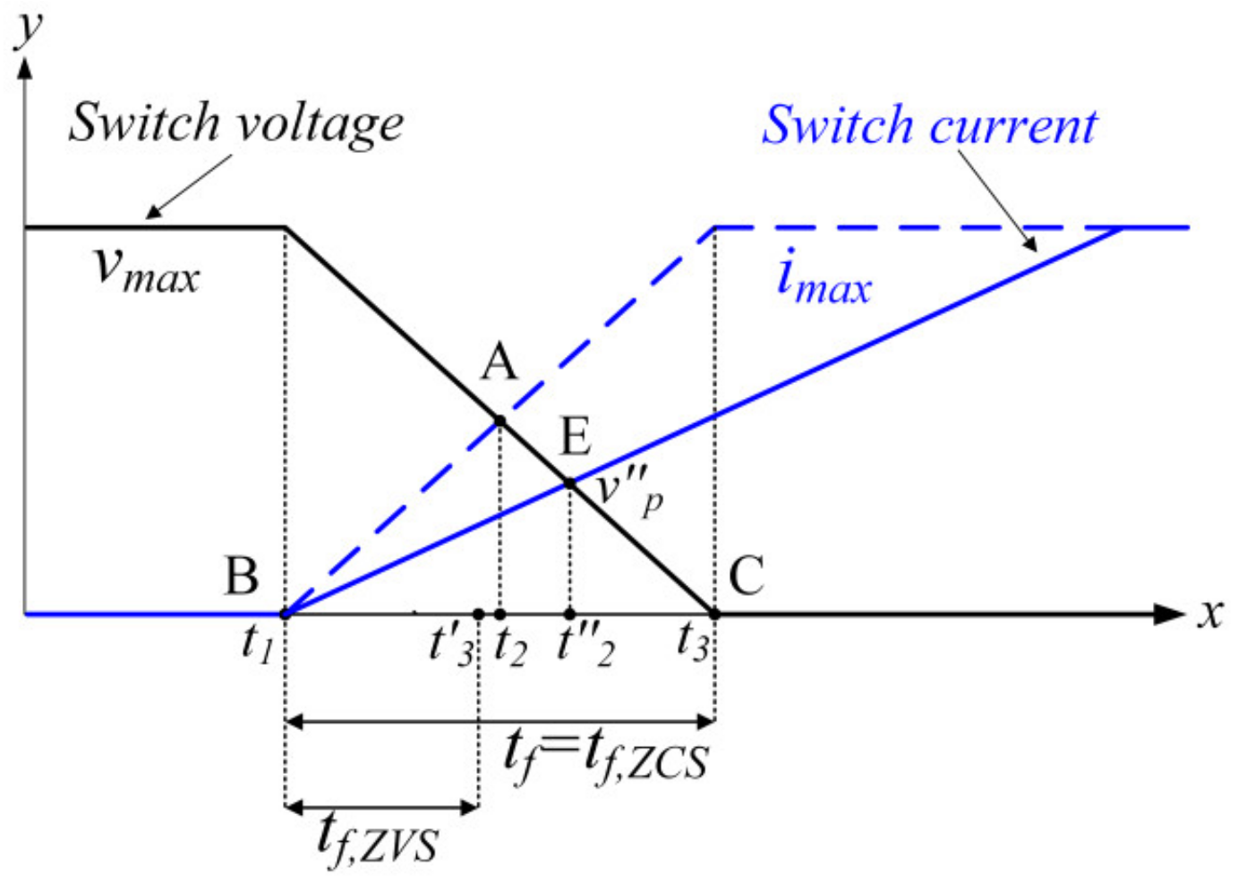
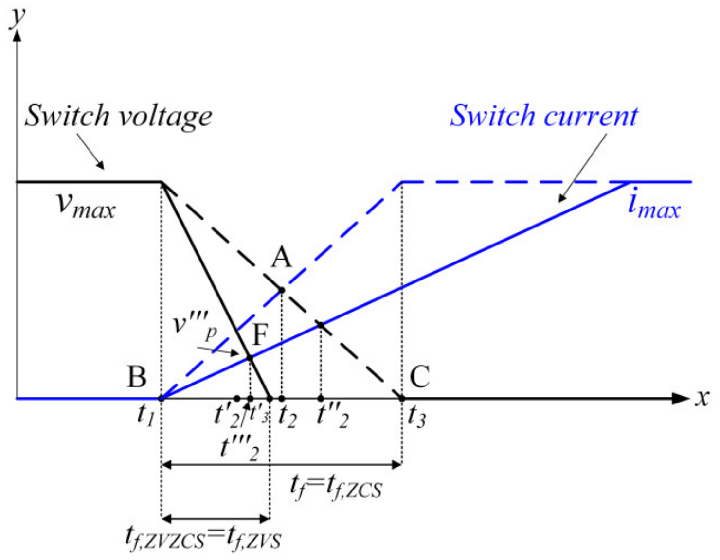
2.4. The True Zero-Voltage Zero-Current Switching

In the ZVZCS mode, both the voltage and the current transients are altered to minimize the crossover as obvious from Figure 8. For this case, as obvious from Figure 9, the voltage and current intersection points move from F to the left of E. This point is located at t 2 on the x-axis which is different from the ZVS intersection point located at t 2 . The switch voltage v can be defined as
v = t t 1 t 3 t 1 v max + v max ,
where t1 < t < t 3 .
Now, v p at t 2 can be defined as
v p = ( t 2 t 1 t 3 t 1 ) ( v max ) + v max .
Consequently, the energy loss can be defined as
E t ZVZCS , t o n l o s s = 0.5 t 3 t 1 t 2 t 1 t 3 t 1 v max + v max ( f s ) = 0.5 v max t f , ZVS t 2 t 2 + t 2 t 1 t f , ZVS + 1 ( f s ) = 0.5 v max t f , ZVS t 2 t 2 + t t f , ZVS + 1 ( f s ) = 0.5 v max t f , ZVS t + x ( f s )
where t 3 t1 = tf,ZVZCS = tf,ZVS and t 2 t1 = t′. Moreover, x is defined as
x = t 2 t 2 .
As F is located to the right of D, x must be positive. Hence, it is obvious from Equations (22) and (25) that the energy loss in the ZVZCS mode is further truncated as compared to the ZVS or ZCS. For the turn off instant, Equation (26) can be rewritten as
E t ZVZCS , t o f f l o s s = 0.5 v max t f , ZVS t + x ( f s ) .
Hence, from Equations (7), (11), (18), and (25), it becomes obvious that the ZVZCS mode switching is more efficient in reducing the energy loss at the turn on point than the ZVS or the ZCS. More specifically, as compared to the ZVS, the ZVZCS reduces the loss in percentage by
E t o n l o s s r e d u c t i o n = E ZVS , t o n l o s s E ZVZCS , t o n l o s s E ZVS , t o n l o s s × 100 = t 2 t f , ZVS + t 1 × 100 .
Roughly, the net loss reduction in percentage at the turn on and turn off should be
E t o t a l l o s s r e d u c t i o n = 1.5 t 2 t f , ZVS + t 1 × 100 .
As compared to the ZCS, the loss reduction can be defined as
E t o n l o s s r e d u c t i o n = E ZCS , t o n l o s s E ZVZCS , t o n l o s s E ZCS , t o n l o s s × 100 = t f , ZVS t 2 t 1 × 100 .
Again, the net loss reduction as compared to the ZCS in percentage should be
E t o t a l l o s s r e d u c t i o n = 1.5 t f , ZVS t 2 t 1 × 100 .
By replacing the parameter values from Figure 9, the energy loss in ZVZCS mode amounts to
E ZVZCS , t o n l o s s = 0.5 × 50 0.5 × 0.7 × 10 6 100 × 10 3 = 875   m W .
Hence, it can be concluded that the ZVZCS is capable of reducing the energy loss at the switch transition points as compared to that induced in the HS, ZVS, or ZCS modes.

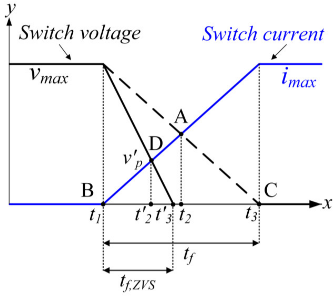
3. Analysis for the Estimation of the Soft Switching Range

3.1. The Zero-Voltage Switching (ZVS)

In the ZVS, the turn on loss is defined in terms of input voltage as
E ZVS , t o n l o s s = 0.5 v max t f , ZVS t ( f s ) .
In terms of switch current, it can be rewritten as
E ZVS , t o n l o s s 0.5 0.25 i max ( ) t f , ZVS | | s .
It can be observed that the ZVS turn on loss largely depends on the maximum applied switch voltage vmax, which is the input voltage for a forward mode converter. This dependency can be reduced if switching frequency (fs) is decreased. However, it is not an effective solution, as reducing the switching frequency would increase the size of the passive components, while the term (tf,ZVSt′) is constant. On the other hand, the dependency on the switch current is much weaker as obvious from Equation (32). Hence, this large dependency on the switch voltage makes the ZVS operation largely vulnerable to the input voltage and duty cycle ratio. Subsequently, the ZVS operation is difficult to maintain for a wide operating window.

3.2. The Zero-Current Switching (ZCS)

In the ZCS, the energy loss in terms of maximum switch voltage (vmax) and current (imax) is described as
E ZCS , t o n l o s s = 0.5 v max t f t 2 t 1 ( f s ) ,
and
E ZCS , t o n l o s s 0.5 i max t f t 2 t 4 ( f s ) .
In Equation (34), as obvious from Figure 6,
t f t 2 t 1 .
Hence, the maximum switch voltage (vmax) has a minimal effect on the ZCS operation. On the contrary, the ZCS operation is largely affected by imax, as can be seen in Equation (35). To reduce this effect, fs has to be minimized as the term ( t 2 /t4) is constant. However, as mentioned earlier, it is not an effective solution as the size of the passive components can increase substantially. The dependency on the switch current makes the ZCS operation vulnerable to the converter loading conditions. Consequently, for wide load variation, the ZCS is difficult to achieve. In other words, the soft switching range of operation is affected.

3.3. The True Zero-Voltage Zero-Current Switching

In this mode, the energy loss terms are
E t ZVZCS , t o n l o s s = 0.5 v max t f , ZVS t + x ( f s ) = 0.5 v max t f , ZVS t 2 t 1 ( f s )
or
E t ZVZCS , t o n l o s s = 0.5 i max t f , ZVS t 2 t 4 ( f s ) .
It can be deduced from Figure 4 that
t f , ZVS t 2 t 1 .
Hence, it is obvious from Equation (37) that the maximum switch voltage has a minimal effect on the true ZVZCS. Similarly, it can be observed from Figure 8 that
t 2 t 4 .
Subsequently, as obvious from Equation (38), the dependency of the ZVZCS operation on the switch current is negligible. Hence, the ZVZCS is not largely affected by the input voltage and loading conditions. In return, it becomes capable of providing a wider soft switching range by remaining operational irrespective of the input voltage and load current conditions.

4. Simulation Results for Comparative Analysis

To prove the theoretical statement, a PSPICE simulation was performed for selected topologies from the recent literature. The converters were simulated in the boost mode and the specifications in Table 2 were maintained.
Furthermore, the converters were intentionally operated at a low power level (i.e., 200 W) for better visualization of the switching losses. The main switches of the converters were taken into consideration to measure the incurred turn on and turn off losses while the converters were operated in (1) the ZVS mode, (2) the ZCS mode, or (3) the ZVZCS mode. The measurement was performed in different states (State A to State F) of the circuit. Each state denoted a unique combination of the switching frequency (fs), the input voltage (VL), and the load current. The variation of the operational states made the results unbiased to the operating conditions of the converter. Furthermore, the measured turn on and turn off losses for different soft switching conditions were averaged to achieve more accurate results. The simulation results are demonstrated in Table 3.
To provide a better visual understanding, the average turn on and turn off losses induced in the ZVS, the ZCS, or the ZVZCS modes are plotted in Figure 10 and Figure 11, respectively, in different operational states. As can be seen, the average turn on loss from State A to F increased from 1200 to 1800 mW, while the turn off loss increased from 550 mW in State A to 850 mW in State F. For the ZCS, the turn on loss in State A was 1400 mW, becoming 1700 mW in State F, while it increased from 700 to 850 mW at turn off. In contrast, in the ZVZCS mode, the turn on loss was 880 mW in State A, increasing to 1300 mW in State F. Moreover, the turn off loss was 450 mW in State A, increasing to 600 mW in State F. On average, the loss at turn on and turn off for the ZVZCS was reduced by 26% and 20%, respectively, as can be deduced from Figure 10 and Figure 11, respectively.
To provide insight into the soft switching range of operation, (1) the average turn on and turn off losses out of all the six states and (2) the cumulated standard deviations from the average values were calculated. The results are shown in Table 4. As can be observed, the ZVZCS incurred the lowest turn on and turn off losses on average. Furthermore, the standard deviation (SD) shows that the deviation from the average was fairly lower for the ZVZCS mode as compared to others. This signifies a stable low-loss profile throughout all six states and proves the superiority of the ZVZCS soft switching performance across the whole operating range.

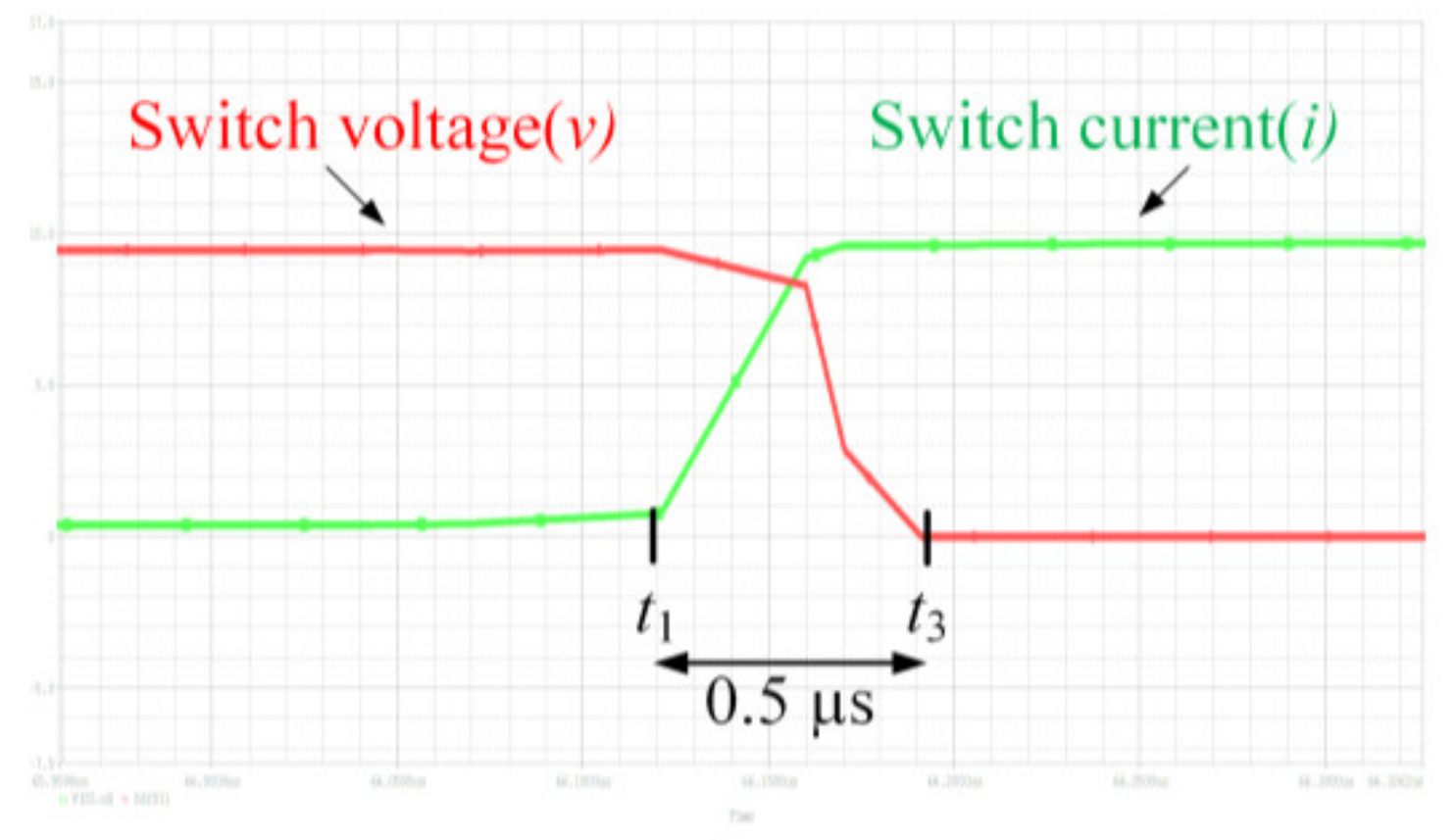
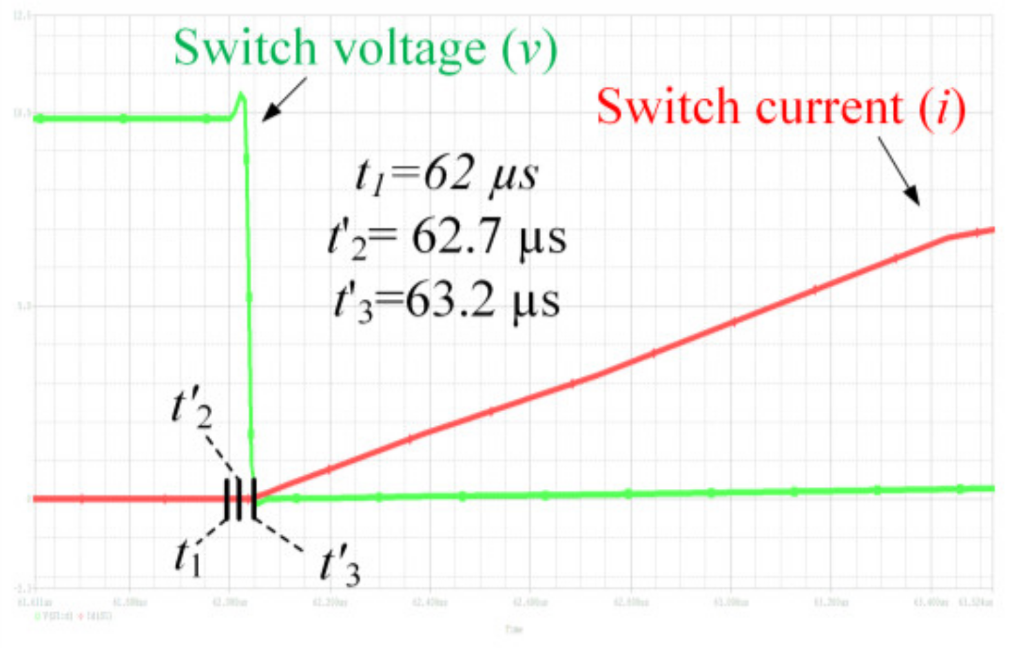
5. Experimental Verification

To verify the theoretical claim, an experimental test was performed. A prototype ZVZCS converter [22] was built to evaluate the switching losses under various soft switching conditions. The simulation waveforms for the prototype converter are demonstrated in Figure 2, Figure 4, Figure 6, and Figure 8 for different switching states. In this section, the experimental test procedure is discussed through a description of the converter operational modes, intervals, and results. Please note that Table 4 represents the average of all turn on and turn off losses obtained by simulating the circuit in six different states (A to F; variation in input voltage, duty ratio, and frequency). However, by operating the circuit in a particular state stated in Table 5, the experimental results are given in Table 6.
It was particularly difficult to design the prototype for optimum operation (ZVS, ZCS, and ZVZCS) in all six states. Hence, a representative result is shown.

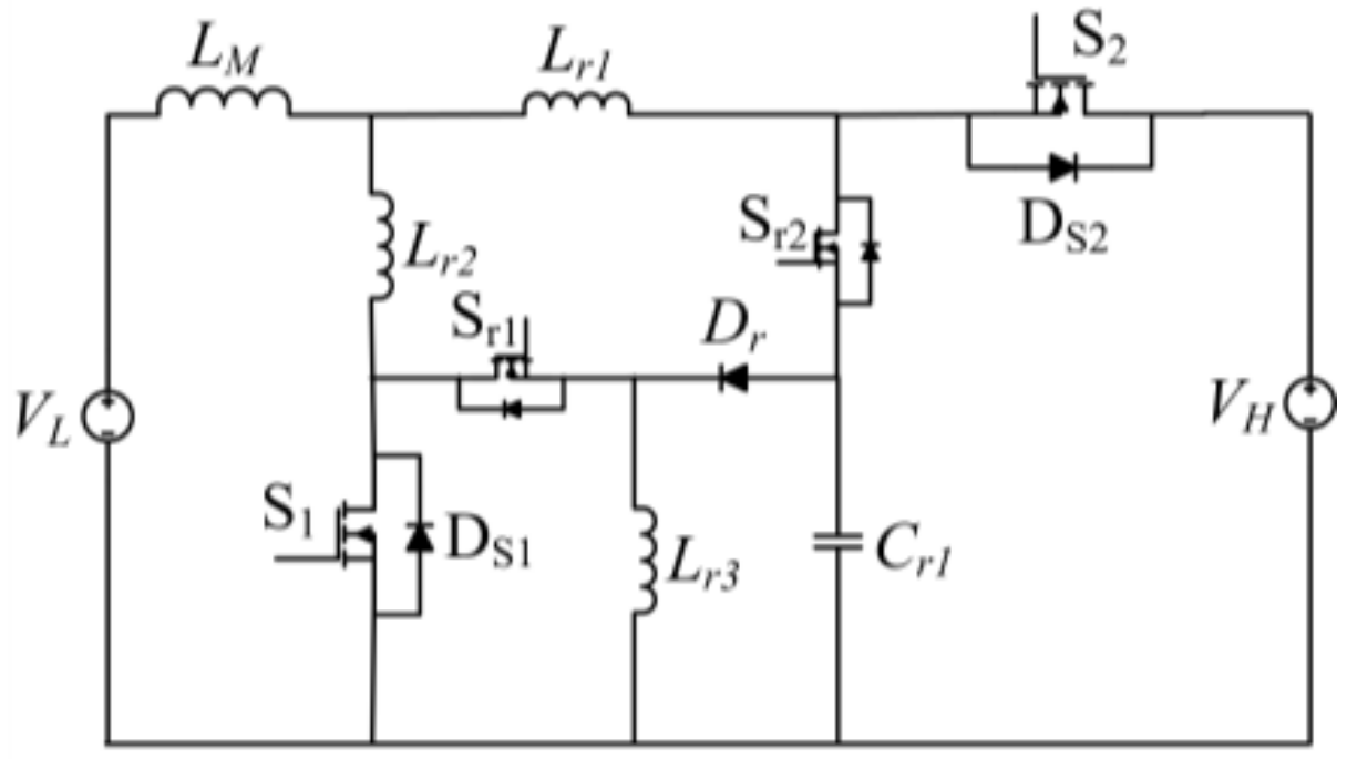
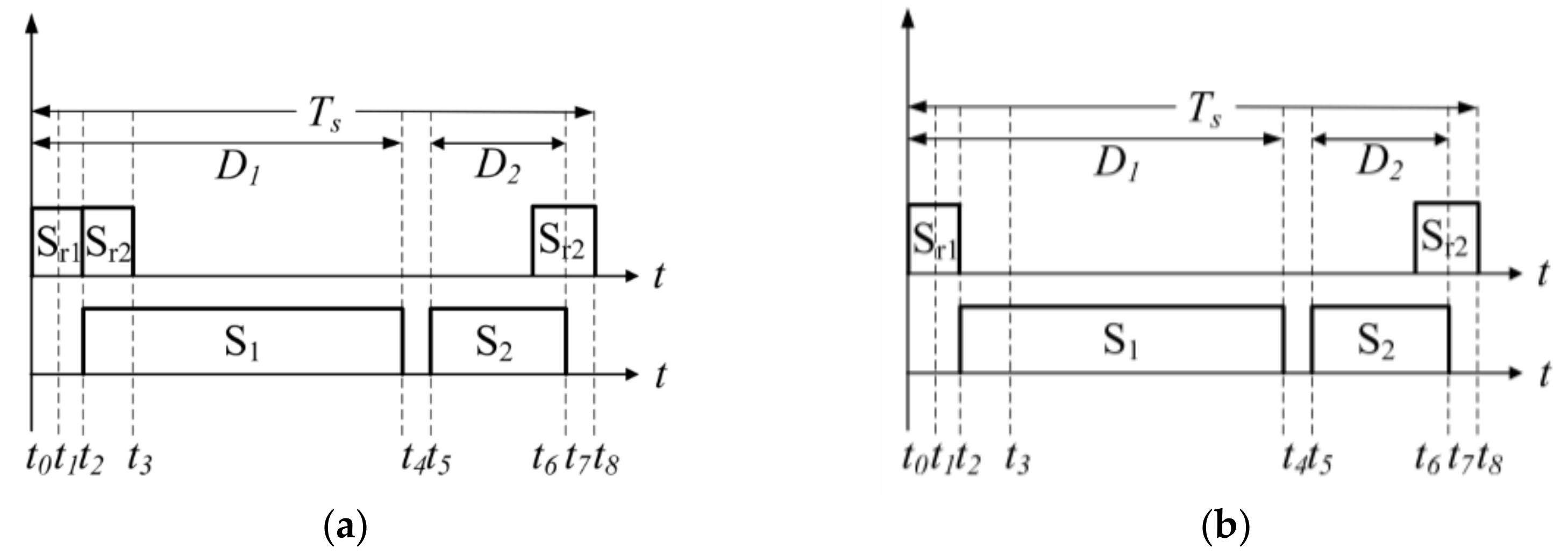
5.1. Converter Topology and PWM Switching

The converter (as shown in Figure 1) consisted of the main switches S1 and S2, the auxiliary switches Sr1 and Sr2, the main inductor LM, the auxiliary inductors Lr1 and Lr2, and the auxiliary capacitor Cr1. It was bidirectional and separately operable in the ZVS, the ZCS, and the ZVZCS modes. For the experimental verification, the converter was tested in the boost mode only, and the turn on and turn off losses were calculated for the main switch S1. For this purpose, the circuit was operated in four different stages:
  • Stage 1: the ZVZCS mode;
  • Stage 2: the ZVS mode;
  • Stage 3: the ZCS mode;
  • Stage 4: the hard switching (HS) mode.
In Stage 1, the turn on and turn off of S1 was conducted in the ZVZCS mode. To achieve this, both the auxiliary switches (Sr1 and Sr2) were turned on, as shown in Figure 12a. This led to the near-zero switching loss at the transitions. In Stage 2, Sr1 was turned on and Sr2 was turned off, as shown in Figure 12b. Consequently, S1 was operated in the ZVS mode. The sharp voltage rise across the switch S1 was controlled by the ZVS mode, by turning on the respective body diode. In Stage 3, to achieve the ZCS at S1, the Sr1 was turned off and Sr2 was turned on, as in Figure 12c. This forced the body diode of S1 to remain turned off. Simultaneously, the Lr2 and the capacitor Cr1 realized the ZCS operation in S1. For this purpose, Lr1 and Lr2 controlled the sharp rise in current through S1. Lastly, in Stage 4, for the hard switching stage, both the auxiliary switches (i.e., Sr1 and Sr2) were turned off, as shown in Figure 12d. To give a general idea of the operation of the circuit, the operational intervals are briefly described below.

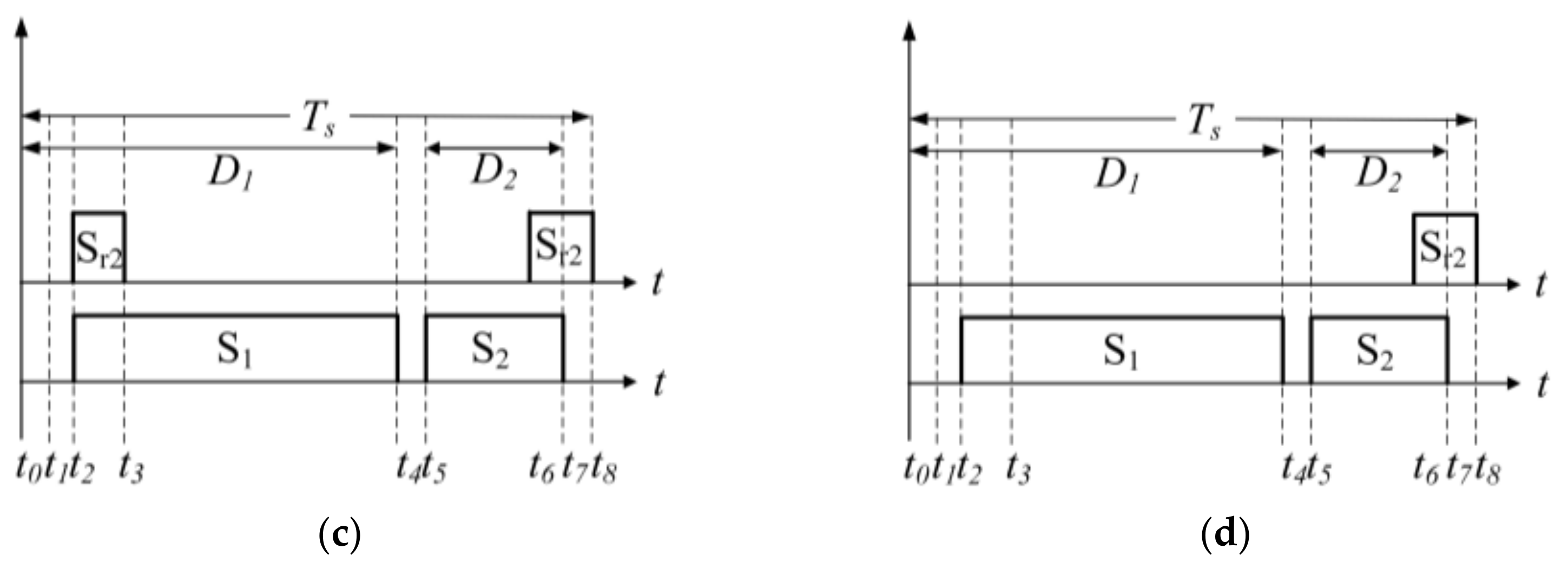
5.2. Converter Operational Intervals

The operational intervals are important to understanding the basic operation of the circuit. Hence, the operational intervals are described briefly, which should be sufficient to understand the soft switching operation.
(a)
Interval 1 [t1t0, Stage 1 + Stage 2]:
At t0, the auxiliary switch Sr1 is turned on in the ZVS mode. The current starts to flow through Sr1 and subsequently charges the resonant inductor Lr3. The capacitor Cr1 turns on the diode Dr and discharges to Lr3 through the diode. Throughout this interval, the inductor current iLM remains constant and discharges to the output. The time interval t10 is determined as
t 10 5 τ S = 5 L r 2 + L r 3 R L r 2 + R L r 3 = 5 L T R T .
(b)
Interval 2 [t2t1, Stage 1+ Stage 2]:
At t1, the body diode of S1 is turned on and Lr3 starts to discharge through it. This, in return, enables S1 to be turned on in the ZVS mode at t2. At t2, the current through the switch Sr1 reaches zero, and Sr1 is turned off in ZCS mode. To allow Lr3 to discharge completely, t21 has to be selected as
t 21 3 τ S = 3 L r 2 + L r 3 R L r 2 + R L r 3 = 3 L T R T .
Combining Equations (41) and (42), the following relationship is obtained:
t 20 8 τ S .
Thus, as long as the lower limit restrictions in Equations (41) and (42) are satisfied, the ZVS condition is achievable. However, to avoid unnecessary losses in the auxiliary components and the body diode of the main switch, the delay should be kept equal to or lower than twice the minimum limit. Hence, the functional range of t20 should be
16 τ S t 20 8 τ S .
(c)
Interval 3 [t3t2, Stage 1 + Stage 3]:
At t2, the switch S1 is turned on in the ZVZCS mode. To achieve this purpose, the inductor Lr2 in series with S1 restricts the sharp rise in current through the switch. In general, as the value of the inductor Lr2 increases, the slope di/dt decreases as obvious from Equation (45). However, excessively large Lr3 would affect the ZVS transition of S1. At t3, Sr2 is turned on for a very short period. Consequently, Cr1 is charged by the reverse recovery current irr. To this purpose, Cr1 is designed to be able to accommodate the reverse recovery charge Qrr.
d i L r 2 d t = V L L r 2 .
(d)
Interval 4 [t4t3, Stage 1–4]:
Throughout this interval, the inductor current iLM continues to increase. At t4, S1 is turned off in the ZVZCS mode.
d i L M d t = V L L M .
(e)
Interval 5 [t5t4, Stage 1–4]:
This interval is kept short enough to avoid any unnecessary current stress on the power switches and simultaneously to avoid the short circuit condition while both S1 and S2 are switched on.
(f)
Interval 6 [t6t5, Stage 1–4]:
At t6, switch S2 is turned on in the ZVZCS mode. Consequently, the inductor LM starts to discharge through S2. The inductor current (iLM) decreases as
d i L M d t = V L V H L M .
(g)
Interval 7 [t8t7, Stage 1–4]:
Throughout this interval, the body diode of S2 remains open. Thus, the inductor LM continues to discharge through the body diode of the switch S2. At the end of this interval, Sr2 is turned off in the ZVS mode. iLM decreases as
d i L M d t = V L V C r 1 L M .

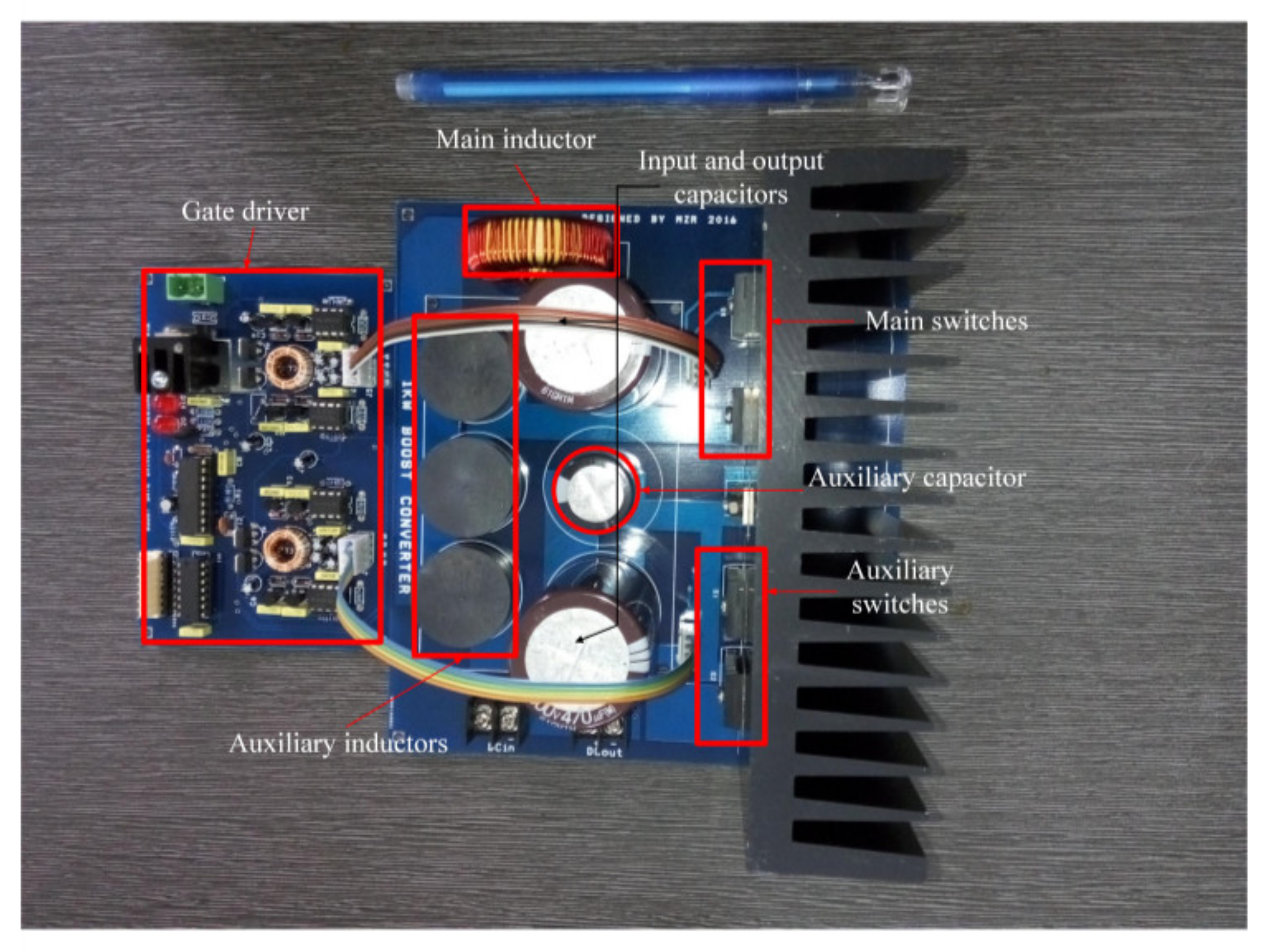
5.3. Experimental Setup

The prototype circuit is shown in Figure 13. The circuit was built according to the specifications in Table 5.
The TMS320F2812 DSP was used to generate PWM pulses. The DSP has 12 PWM channels and 150 MHz clock frequency. Both the high- and the low-voltage-side power transistors were implemented with an IPW50R190CE (550 V, 63 A, Rds (on) = 190 mΩ) MOSFET. The low-power auxiliary switches were implemented with an FDP15N40 (400 V, 15 A, Rds (on) = 300 mΩ) MOSFET. The ITECH IT8816B DC electronic load was used for testing purposes. The converter was operated at approximately 0.3 to 0.4 duty cycle ratio. Please note that a slight change was made for various switching profiles to ensure minimum energy loss; thus ensuring a fair comparison for ZVS, ZCS, or ZVZCS capabilities. Note that the switching profiles are also different for the prototype converter for ZVS, ZCS, and ZVZCS; hence, the change in duty ratio can be justified for the optimum operation of the converter itself.

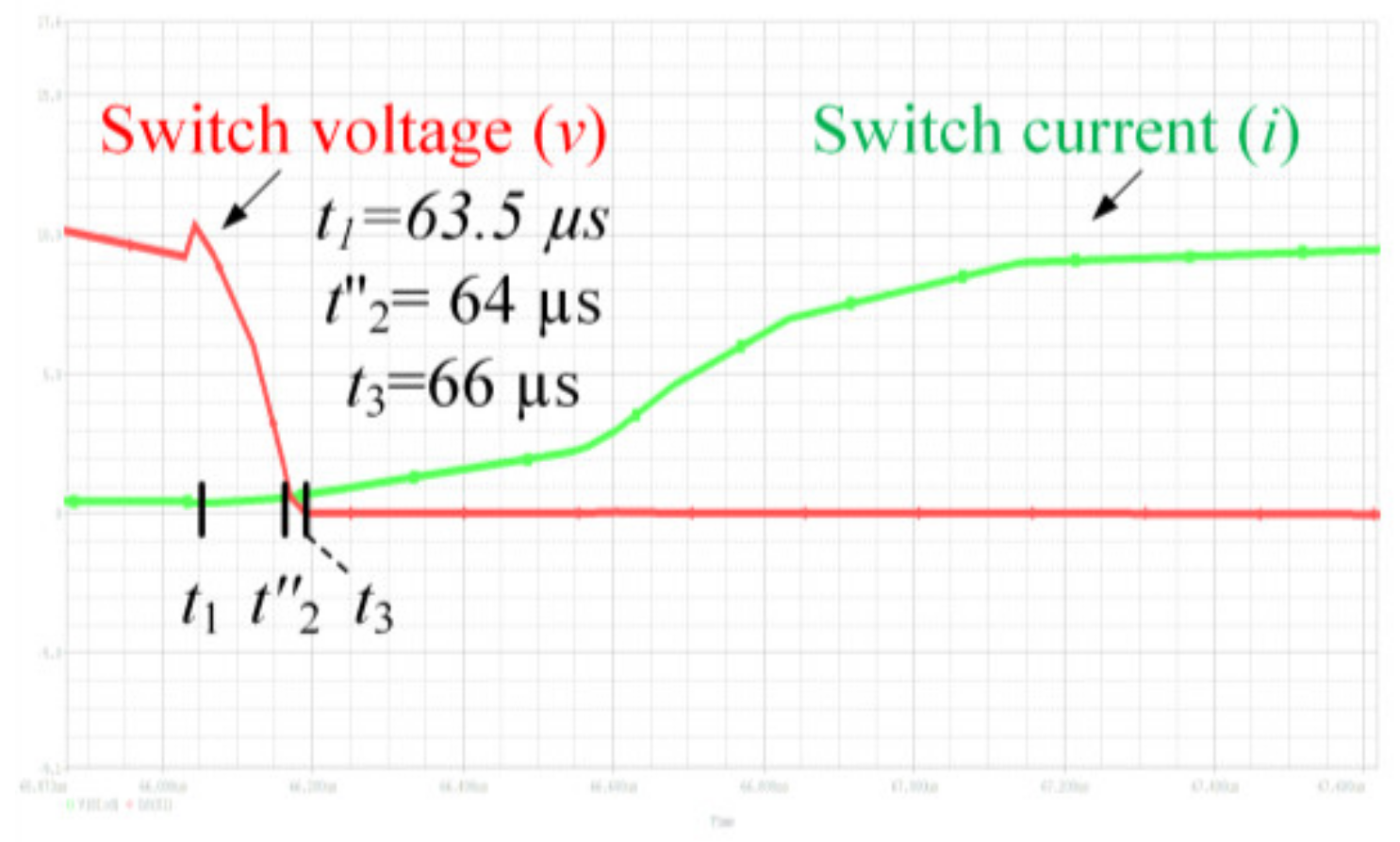
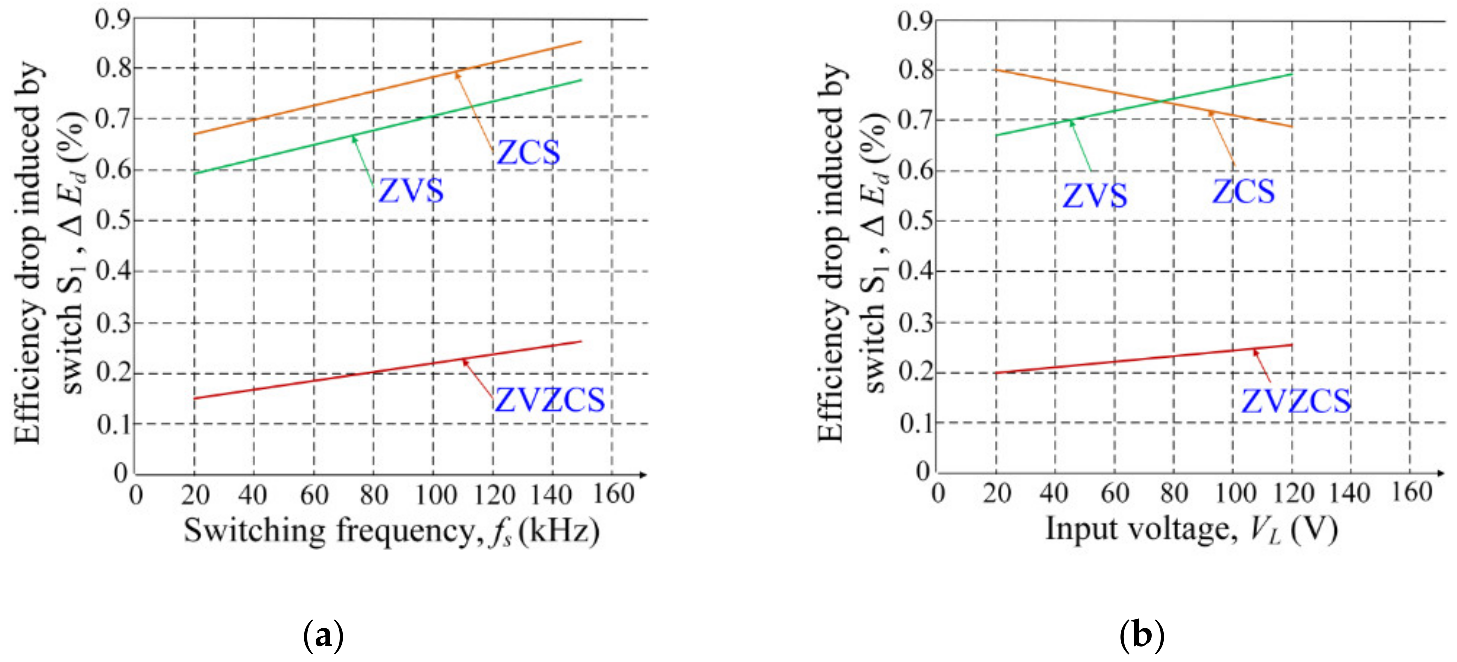
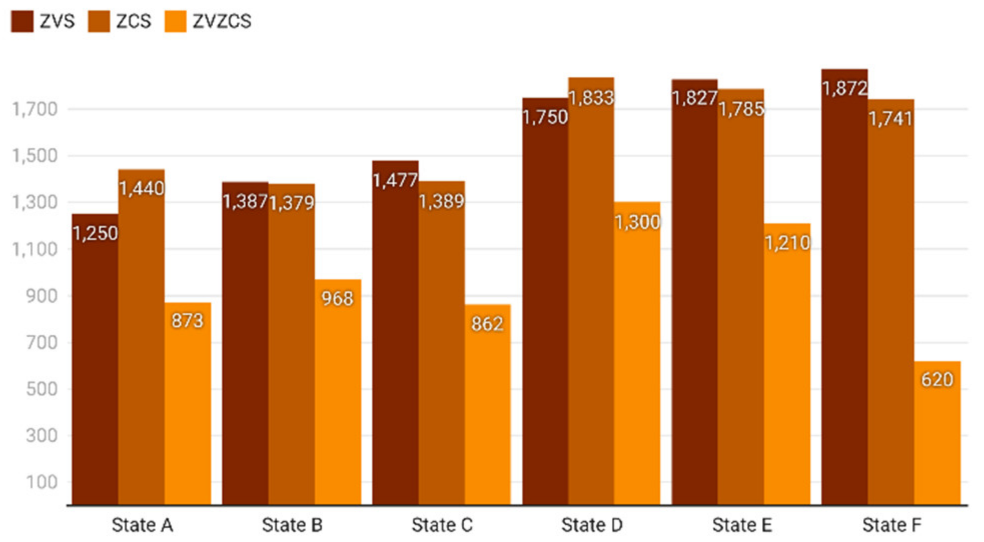
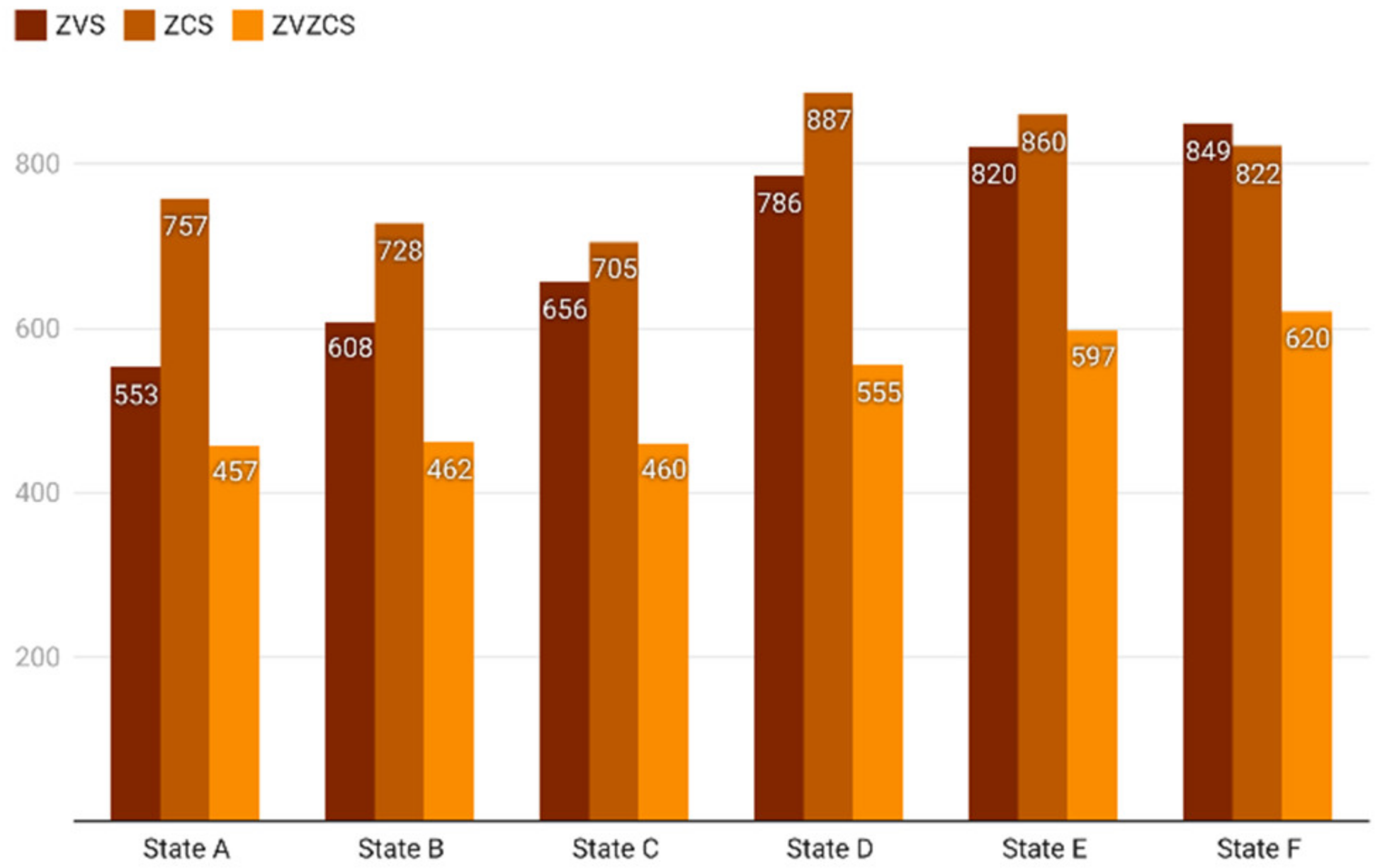
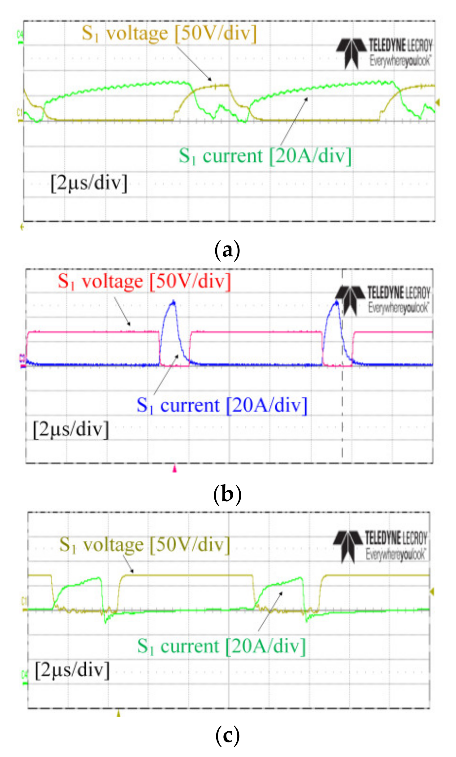
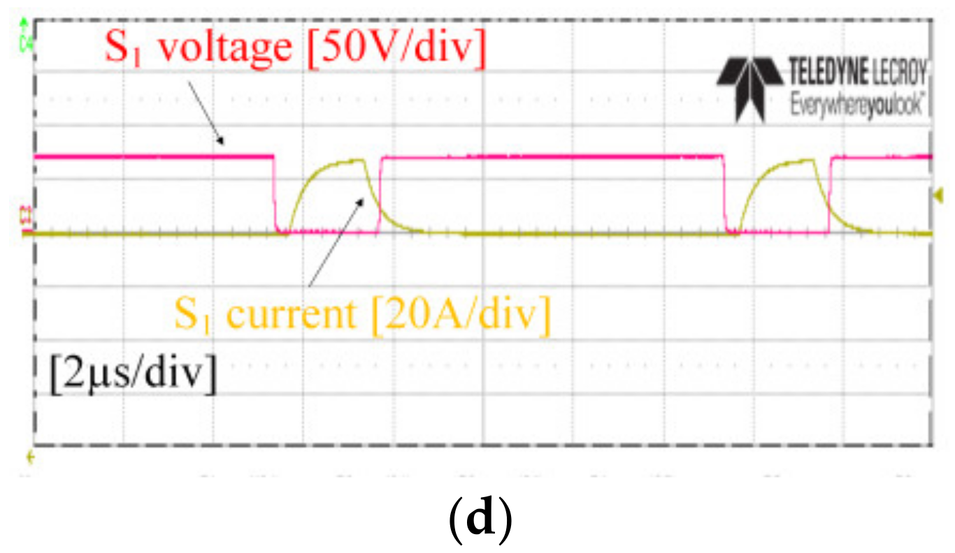
5.4. Results and Discussion

For all cases, the switching losses were measured in switch S1. In Figure 14, the voltage and current waveforms of S1 are shown for different switching conditions. The measured losses are given in Table 6. It can be observed from Table 4 that the ZVS and ZCS improved the switching states and reduced the losses compared to the hard switching condition by more than 30%. However, the improvement induced by the ZVZCS operation from the HS counterpart was more than 80%, which surpasses other soft switching conditions. Thus, the efficiency was largely improved.
The efficiency improvement in the ZVZCS mode could be easily identified as stated in Table 7. As can be seen, the efficiency drop was reduced from 2.30% in the hard switching mode to 0.23% in the ZVZCS mode. This signifies an average of 2% improvement in the efficiency of the converter imposed by the ZVZCS operation of the main switch only. Hence, it can be safely concluded that the experimental results are well in accordance with the theoretical claim.
The percentage drop in efficiency imposed by the switch S1 was measured by varying the switching frequency (fs) and the input voltage (VL) at Stages 1, 2, and 3. For this purpose, fs was varied from 20 to 150 kHz, while VL was kept constant at 80 V and PO = 150 W. On the other hand, VL was varied from 20 to 120 V, while fs was kept constant at 100 kHz and PO = 150 W. The results are demonstrated in Figure 15, respectively. As obvious, the efficiency drop in the ZVZCS mode remained consistently lower and was more stable throughout the operating conditions (i.e., variation in fs and VL). For example, as can be seen in Figure 15a, ΔEd = 0.2%, 0.2%, and 0.1% for the ZVS, ZCS, and ZVZCS, respectively. Similarly, it was 0.15%, 0.15%, and 0.05% for the ZVS, ZCS, and the ZVZCS, respectively, as shown in Figure 15b. Consequently, wider soft switching operating range in the ZVZCS mode was ensured.

6. Conclusions

In this paper, the ZVZCS soft switching technique was analyzed. A theoretical analysis was provided to demonstrate the superiority of the ZVZCS to the ZVS and the ZCS in reducing the switching losses and improving the soft switching range of operation. It was found that the improvement was primarily because of the ZVZCS not being largely affected by the factors that affect the ZVS turn on (i.e., the input voltage) and the ZCS (i.e., the load current) turn off operations. To support the theoretical claim, a simulation test was performed on several soft switching converters from the recent literature. The converters were tested in different operational states to ensure unbiased results. The turn on and turn off losses were then measured in the main switches. It was observed that the induced losses were reduced for the ZVZCS operation, which amounted to 26% and 20% reductions compared to the ZVS and the ZCS counterparts, respectively. Furthermore, the low standard deviation for the ZVZCS operation denoted minimal deviation from the average loss profile throughout the operational states. Thus, a stable low-loss profile rendering a wider soft switching range was ensured. On top of that, a prototype soft switching converter was built to perform the experimental test. The converter was independently operable in different soft switching conditions (i.e., the HS, the ZVS, the ZCS, and the ZVZCS). Subsequently, the incurred turn on and turns off losses in the main switch were measured under these conditions. Overall, it was observed that the ZVZCS mode reduced the switching losses as compared to the HS, the ZVS or the ZCS and helped to further improve the converter efficiency. Moreover, it was found that the efficiency drop remained consistently low and stable while measured against the variation of switching frequency and input voltage. This proved the wider operability of the ZVZCS over the ZVS and the ZCS modes. In future work, the higher efficiency and wider operability of ZVZCS over other similar techniques can be further verified for a range of different converter types.

Author Contributions

Conceptualization, R.H.A.; data curation, M.H.M. and Z.S.; formal analysis, A.S., M.T.I. and M.F.R.; funding acquisition, P.K.; investigation, M.T.I.; methodology, R.H.A. and Z.S.; project administration, A.S. and H.H.F.; resources, H.H.F.; software, M.H.M.; validation, R.H.A.; visualization, R.H.A.; writing—original draft, R.H.A.; writing—review and editing, P.K., H.H.F. All authors have read and agreed to the published version of the manuscript.

Funding

This research received no external funding.

Conflicts of Interest

The authors declare no conflict of interest.

References

  1. Chien-Ming, W. A New Family of Zero-Current-Switching (ZCS) PWM Converters. IEEE Trans. Ind. Electron. 2005, 52, 1117–1125. [Google Scholar] [CrossRef]
  2. Mohammadi, M.; Adib, E.; Yazdani, M.R. Family of Soft-Switching Single-Switch PWM Converters With Lossless Passive Snubber. IEEE Trans. Ind. Electron. 2015, 62, 3473–3481. [Google Scholar] [CrossRef]
  3. Mohammadi, M.R.; Farzanehfard, H. A New Family of Zero-Voltage-Transition Nonisolated Bidirectional Converters With Simple Auxiliary Circuit. IEEE Trans. Ind. Electron. 2016, 63, 1519–1527. [Google Scholar] [CrossRef]
  4. Dusmez, S.; Khaligh, A.; Hasanzadeh, A. A Zero-Voltage-Transition Bidirectional DC/DC Converter. Ind. Electron. IEEE Trans. 2015, 62, 3152–3162. [Google Scholar] [CrossRef]
  5. Mishima, T.; Nakaoka, M. A Practical ZCS-PWM Boost DC-DC Converter With Clamping Diode-Assisted Active Edge-Resonant Cell and Its Extended Topologies. IEEE Trans. Ind. Electron. 2013, 60, 2225–2236. [Google Scholar] [CrossRef]
  6. Zhang, J.; Lai, J.-S.; Kim, R.-Y.; Yu, W. High-power density design of a soft-switching high-power bidirectional dc–dc converter. Power Electron. IEEE Trans. 2007, 22, 1145–1153. [Google Scholar] [CrossRef]
  7. Ashique, R.H.; Salam, Z.; Aziz, M.J.A. A high power density soft switching bidirectional converter using unified resonant circuit. In Proceedings of the 2015 IEEE Conference on Energy Conversion (CENCON), Johor Bahru, Malaysia, 19–20 October 2015; pp. 165–170. [Google Scholar]
  8. Han, D.-W.; Lee, H.-J.; Shin, S.-C.; Kim, J.-G.; Jung, Y.-C.; Won, C.-Y. A new soft switching ZVT boost converter using auxiliary resonant circuit. In Proceedings of the 2012 IEEE Conference on Vehicle Power and Propulsion Conference (VPPC), Seoul, Korea, 9–12 October 2012; pp. 1250–1255. [Google Scholar]
  9. Ivanovic, B.; Stojiljkovic, Z. A novel active soft switching snubber designed for boost converter. IEEE Trans. Power Electron. 2004, 19, 658–665. [Google Scholar] [CrossRef]
  10. Mishima, T.; Nakaoka, M. A new family of soft switching PWM non-isolated DC-DC converters with Active auxiliary Edge-Resonant Cell. In Proceedings of the 2010 International Power Electronics Conference (IPEC), Sapporo, Japan, 21–24 June 2010; pp. 2804–2809. [Google Scholar]
  11. Patil, D.; Rathore, A.K.; Srinivasan, D. A non-isolated bidirectional soft switching current fed LCL resonant dc/dc converter to interface energy storage in DC microgrid. In Proceedings of the 2015 IEEE Applied Power Electronics Conference and Exposition (APEC), Charlotte, NC, USA, 15–9 March 2015; pp. 709–716. [Google Scholar]
  12. Rathore, A.K.; Patil, D.R.; Srinivasan, D. A Non-Isolated Bidirectional Soft Switching Current fed LCL Resonant DC/DC Converter to Interface Energy Storage in DC Microgrid. Ind. Appl. IEEE Trans. 2015, 52, 1711–1722. [Google Scholar] [CrossRef]
  13. Ahmadi, M.; Mohammadi, M.R.; Adib, E.; Farzanehfard, H. Family of non-isolated zero current transition bi-directional converters with one auxiliary switch. IET Power Electron. 2012, 5, 158–165. [Google Scholar] [CrossRef]
  14. Ardi, H.; Ahrabi, R.R.; Ravadanegh, S.N. Non-isolated bidirectional DC–DC converter analysis and implementation. IET Power Electron. 2014, 7, 3033–3044. [Google Scholar] [CrossRef]
  15. Sanchis-Kilders, E.; Ferreres, A.; Maset, E.; Ejea, J.B.; Esteve, V.; Jordan, J.; Calvente, J.; Garrigos, A. Bidirectional high-power high-efficiency non-isolated step-up dc-dc converter. In Proceedings of the 37th IEEE Power Electronics Specialists Conference, Jeju, Korea, 18–22 June 2006; pp. 1–7. [Google Scholar]
  16. Akin, B. An Improved ZVT–ZCT PWM DC–DC Boost Converter With Increased Efficiency. Power Electron. IEEE Trans. 2014, 29, 1919–1926. [Google Scholar] [CrossRef]
  17. Aksoy, I.; Bodur, H.; Bakan, A.F. A New ZVT-ZCT-PWM DC–DC Converter. IEEE Trans. Power Electron. 2010, 25, 2093–2105. [Google Scholar] [CrossRef]
  18. Bodur, H.; Bakan, A.F. A new ZVT-ZCT-PWM DC-DC converter. Power Electron. IEEE Trans. 2004, 19, 676–684. [Google Scholar] [CrossRef]
  19. Ashique, R.H.; Shihavuddin, A.S.M.; Khan, M.M.; Islam, A.; Ahmed, J.; Arif, M.; Maruf, M.H.; Mansur, A.A.; Haq, M.A.U.; Siddiquee, A. An Analysis and Modeling of the Class-E Inverter for ZVS/ZVDS at Any Duty Ratio with High Input Ripple Current. Electronics 2021, 10, 1312. [Google Scholar] [CrossRef]
  20. De Oliveira Stein, C.M.; Hey, H.L. A true ZCZVT commutation cell for PWM converters. Power Electron. IEEE Trans. 2000, 15, 185–193. [Google Scholar] [CrossRef] [Green Version]
  21. Urgun, S. Zero-voltage transition–zero-current transition pulsewidth modulation DC–DC buck converter with zero-voltage switching–zero-current switching auxiliary circuit. Power Electron. IET 2012, 5, 627–634. [Google Scholar] [CrossRef]
  22. Ashique, R.H.; Salam, Z. A Family of True Zero Voltage Zero Current Switching (ZVZCS) Non-isolated Bidirectional DC-DC Converter with Wide Soft Switching Range. IEEE Trans. Ind. Electron. 2017, 64, 5416–5427. [Google Scholar] [CrossRef]
  23. Stein, C.D.O.; Hey, H.L. A true ZCZVT commutation cell for PWM converters. In Proceedings of the APEC’98 Thirteenth Annual Applied Power Electronics Conference and Exposition, Anaheim, CA, USA, 15–19 February 1998; pp. 1070–1076. [Google Scholar]
  24. Mohammad, K.; Ahad, A.; bin Arif, M.S.; Ashique, R.H. Critical Analysis and Performance Evaluation of Solar PV-System Implementing Non-Isolated DC-DC Converters. In Proceedings of the 2021 3rd International Conference on Sustainable Technologies for Industry 4.0 (STI), IEEE, Dhaka, Bangladesh, 18–19 December 2021; pp. 1–6. [Google Scholar]
  25. Ashique, R.H.; Maruf, M.H.; Sourov, K.M.S.H.; Islam, M.M.; Islam, A.; Rabbani, M.; Islam, R.M.; Khan, M.M.; Shihavuddin, A.S.M. A Comparative Performance Analysis of Zero Voltage Switching Class E and Selected Enhanced Class E Inverters. Electronics 2021, 10, 2226. [Google Scholar] [CrossRef]
Figure 1. The schematic of the ZVZCS converter under test [22].
Electronics 11 01062 g001
Figure 2. Simulated waveform at HS turn on instant for the prototype converter.
Electronics 11 01062 g002
Figure 3. Linearized hard switching (HS) crossover at turn on instant for theoretical analysis.
Electronics 11 01062 g003
Figure 4. Simulated waveform at the ZVS mode at turn on instant for the prototype converter.
Electronics 11 01062 g004
Figure 5. Linearized zero-voltage switching (ZVS) crossover at turn on instant for theoretical analysis.
Electronics 11 01062 g005
Figure 6. Linearized zero-current switching (ZCS) crossover at turn on instant for theoretical analysis.
Electronics 11 01062 g006
Figure 7. Simulated waveform at the ZCS mode turn on instant for the prototype converter.
Electronics 11 01062 g007
Figure 8. Linearized zero-voltage zero-current switching (ZVZCS) crossover at turn on instant for theoretical analysis.
Electronics 11 01062 g008
Figure 9. Simulated waveform at the ZVZCS mode turn on instant for the prototype converter.
Electronics 11 01062 g009
Figure 10. Average turn on loss in the main switch in mW at different states.
Electronics 11 01062 g010
Figure 11. Average turn off loss in the main switch in mW at different states.
Electronics 11 01062 g011
Figure 12. PWM switching in (a) Stage 1, (b) Stage 2, (c) Stage 3, and (d) Stage 4.
Electronics 11 01062 g012aElectronics 11 01062 g012b
Figure 13. Experimental prototype circuit.
Electronics 11 01062 g013
Figure 14. Voltage and current waveforms of S1 under the (a) HS, (b) ZVS, (c) ZCS, and (d) true ZVZCS conditions.
Electronics 11 01062 g014aElectronics 11 01062 g014b
Figure 15. Efficiency drop imposed by switch S1 against (a) fs and (b) VL.
Electronics 11 01062 g015
Table 1. Specifications for LTPICE simulation of the prototype converter.
ParameterValue/Model
Mode of operationBoost
POUT200 W
LM500 µH
fs100 kHz
VL50 V
VH100 V
Lr1, Lr20.47 µH
Lr30.10 µH
Cr1100 µF
CL, CH470 µF
Table 2. Common specifications.
ParameterValue/Model
Mode of operationBoost
POUT200 W
LM500 µH
All switchesMOSFET IRF150
Table 3. Turn on and turn off loss in the main switch.
State A: fS = 50 kHz, POUT = 200 W, VL = 50 V
Refs. for Simulated
Topology
Soft Switching ModeLoss (mW)
Turn OnTurn OffTurn OnTurn Off
[4]ZVSZVS1200500
[6]ZVSZVS1400650
[3]ZVSZVS1150520
[1]ZCSZCS1480780
[5]ZCSZCS1450745
[13]ZCSZCS1440745
[2]ZCSZVS1390540
[23]ZVZCSZVZCS950520
[24]ZVZCSZVZCS850440
[25]ZVZCSZVZCS820410
State B: fS = 50 kHz, POUT = 200 W, VL = 100 V
[4]ZVSZVS1350550
[6]ZVSZVS1480690
[3]ZVSZVS1330560
[1]ZCSZCS1405750
[5]ZCSZCS1380710
[13]ZCSZCS1390725
[2] ZCSZVS1340630
[23]ZVZCSZVZCS1080550
[24]ZVZCSZVZCS950480
[25]ZVZCSZVZCS875355
State C: fS = 50 kHz, POUT = 200 W, VL = 150 V
[4]ZVSZVS1470620
[6]ZVSZVS1540730
[3]ZVSZVS1420580
[1]ZCSZCS1380720
[5]ZCSZCS1305690
[13]ZCSZCS1355705
[2]ZCSZVS1515695
[23]ZVZCSZVZCS920515
[24]ZVZCSZVZCS880440
[25]ZVZCSZVZCS785425
State D: fS = 100 kHz, POUT = 200 W, VL = 50 V
[4]ZVSZVS1750760
[6]ZVSZVS1820840
[3]ZVSZVS1680740
[1]ZCSZCS1850950
[5]ZCSZCS1810870
[13]ZCSZCS1830840
[2]ZCSZVS1840805
[23]ZVZCSZVZCS1345615
[24]ZVZCSZVZCS1285550
[25]ZVZCSZVZCS1270500
State E: fS = 100 kHz, POUT = 200 W, VL = 100 V
[4]ZVSZVS1820810
[6]ZVSZVS1880870
[3]ZVSZVS1780750
[1]ZCSZCS1780920
[5]ZCSZCS1785840
[13]ZCSZCS1790820
[2]ZCSZVS1785850
[23]ZVZCSZVZCS1265675
[24]ZVZCSZVZCS1200590
[25]ZVZCSZVZCS1165525
State F: fS = 100 kHz, POUT = 200 W, VL = 150 V
[4]ZVSZVS1860830
[6]ZVSZVS1950920
[3]ZVSZVS1805780
[1]ZCSZCS1745880
[5]ZCSZCS1735800
[13]ZCSZCS1755785
[2]ZCSZVS1730865
[23]ZVZCSZVZCS1395685
[24]ZVZCSZVZCS1320620
[25]ZVZCSZVZCS1285555
Table 4. Average turn on and turn off losses in all six states.
Soft Switching ModeAverage Loss (mW)Standard Deviation
Turn OnTurn OffTurn OnTurn Off
ZVS1570690241.98109.45
ZCS1585770193.8376.46
ZVZCS1080520197.2268.58
Table 5. Circuit parameter values.
ParameterValue
PO150 W
LM1000 µH
fs100 kHz
VL50 V
VH120 V
Lr1, Lr20.47 µH
Lr30.10 µH
Cr1100 µF
CL, CH470 µF
Table 6. Loss in switch S1.
Switching ModeTurn On Loss in S1
(mW)
Turn Off Loss in S1
(mW)
Hard16001850
ZVS620400
ZCS680480
ZVZCS160180
Table 7. Total loss and efficiency drop in S1.
Switching ModeTotal Switching Loss (Turn On + Turn Off) in S1
(mW)
Efficiency Drop
(%)
Hard34502.30
ZVS10200.70
ZCS3200.78
ZVZCS1400.23
Publisher’s Note: MDPI stays neutral with regard to jurisdictional claims in published maps and institutional affiliations.

