
Graphene as a Piezoresistive Material in Strain Sensing Applications
by
 , , , ,
Farid Sayar Irani
1 ,
,
Ali Hosseinpour Shafaghi
1,
Melih Can Tasdelen
1,
Tugce Delipinar
1,
Ceyda Elcin Kaya
2,
Guney Guven Yapici
3 and
Murat Kaya Yapici
1,4,5,* 1
Faculty of Engineering and Natural Sciences, Sabanci University, Istanbul TR 34956, Turkey
2
Department of Electrical and Computer Engineering, University of Tulsa, Tulsa, OK 74104, USA
3
Department of Mechanical Engineering, Ozyegin University, Istanbul TR 34794, Turkey
4
Department of Electrical Engineering, University of Washington, Seattle, WA 98195, USA
5
SUNUM Nanotechnology Research Center, Istanbul TR 34956, Turkey
*
Author to whom correspondence should be addressed.
Micromachines 2022, 13(1), 119; https://doi.org/10.3390/mi13010119
Submission received: 14 July 2021
/
Revised: 23 December 2021
/
Accepted: 28 December 2021
/
Published: 12 January 2022
(This article belongs to the Special Issue Feature Papers of Micromachines in Materials and Processing 2021)
Abstract
:High accuracy measurement of mechanical strain is critical and broadly practiced in several application areas including structural health monitoring, industrial process control, manufacturing, avionics and the automotive industry, to name a few. Strain sensors, otherwise known as strain gauges, are fueled by various nanomaterials, among which graphene has attracted great interest in recent years, due to its unique electro-mechanical characteristics. Graphene shows not only exceptional physical properties but also has remarkable mechanical properties, such as piezoresistivity, which makes it a perfect candidate for strain sensing applications. In the present review, we provide an in-depth overview of the latest studies focusing on graphene and its strain sensing mechanism along with various applications. We start by providing a description of the fundamental properties, synthesis techniques and characterization methods of graphene, and then build forward to the discussion of numerous types of graphene-based strain sensors with side-by-side tabular comparison in terms of figures-of-merit, including strain range and sensitivity, otherwise referred to as the gauge factor. We demonstrate the material synthesis, device fabrication and integration challenges for researchers to achieve both wide strain range and high sensitivity in graphene-based strain sensors. Last of all, several applications of graphene-based strain sensors for different purposes are described. All in all, the evolutionary process of graphene-based strain sensors in recent years, as well as the upcoming challenges and future directions for emerging studies are highlighted.
1. Introduction
With the advent of the internet-of-things (IoT), smart, ubiquitous, pervasive sensing is rapidly gaining importance for providing reliable information at unprecedented sensitivity to enable new applications in consumer electronics [1,2,3], healthcare [4,5,6], manufacturing and structural monitoring [7,8], transportation [9,10], defense and surveillance [11,12,13]; as well as to fuel research in fundamental, applied and translational science [14]. Among the various physical measurands, the monitoring of strain finds use in numerous applications and industrial products where the fundamental detection principle relies on the change in electrical properties of the strain sensing element as a result of applied pressure or force. Strain sensors essentially rely on four fundamental sensing modalities which are capacitive, piezoelectric, piezoresistive and optical sensing [15]. Among these, piezoresistive sensors, with their low-cost-fabrication and easy data analysis advantages, have gathered significant attention.
Typically, sensors based on piezoresistivity rely on transducing external mechanical loading into resistance change, which usually follows a linear relationship [16]. Commonly, piezoresistive sensors harness the piezoresistive effect of the sensing material whereby its conductance changes with applied strain, along with change in resistance of the entire sensor assembly due to geometry change upon deformation. To design high-performance piezoresistive sensors, different parameters such as stretchability, sensitivity, dynamic range, limit of detection, accuracy, response speed, stability, durability, fabrication cost and simplicity should be considered. Out of these design criteria, the fundamental figure-of-merit for a strain sensor is its sensitivity, which is evaluated by the gauge factor (GF), formally defined as the ratio of relative resistance change in the sensing element to the mechanical strain acting on it (GF = ΔR/R/ε).
To date, various materials have been investigated for use as strain sensing elements, in an effort to optimize the response of the strain sensor with respect to the attributes mentioned above. Realizing a strain sensor operating at a wide strain range with good sensitivity has been an especially huge challenge. To overcome the problem of low sensitivity, different approaches have been proposed including doping, defect deformation and exploiting different piezoresistive sensing mechanisms along with sensing materials [17,18,19,20,21].
Among the most typical strain sensing materials are metals. However, strain sensors based on metals, otherwise known as metal-foil gauges, primarily rely on resistance change due to dimensional change of electrically conducting thin lines typically structured in the form of a serpentine, and as such the gauge factors are typically limited to single digits [14,22]. Several other strain sensors with different types of semiconductor piezoresistive materials, including doped polysilicon have also been developed, which offer much higher gauge factors compared to metal-foil counterparts [23].
As an alternative to some of these conventional materials like metals, metal oxides, semiconductors and ceramics which suffer either from intrinsic hardness, brittleness, low strain range or poor scalability, in recent years, carbon-based materials have been on the forefront of “sensor research”, including strain sensing [21,22,23,24,25]. As such, nanomaterials including carbon nanotubes (CNT) and graphene have both been reported as functional materials to realize strain sensors [24]. While CNTs have an almost one-dimensional (1D) structure [25], graphene has an ideal two-dimensional (2D) structure which potentially allows conventional device fabrication by planar, semiconductor process technologies. Additionally, its piezoresistive property [26,27] together with its exceptional physical, electrical [28] and mechanical properties (Young’s modulus on the order of 1 TPa) [29] render graphene an ideal candidate for strain sensors [30].
To date, there have been multiple studies which have reported graphene-based strain sensors built on a variety of substrates; however, the fabricated strain sensors display a wide range of gauge factors [31,32,33,34,35,36], making it inconclusive to verify the eventual advantages of graphene over standard metal-foil gauges suffering from low gauge factors. We argue that such variation in performance of graphene-based strain sensors is largely due to the problems in obtaining high-quality graphene, in a repeatable, uniform, scalable fashion and one that allows semiconductor process integration. Therefore, the intention of the present review on graphene-based strain sensors is to provide a critical perspective and discussion on the existing problems preventing the transition of “graphene strain sensors” into actual commercialization which are very much tied to: (a) the technology with which graphene is obtained, and (b) the integration of graphene into a realistic device topology.
Along these lines, in this work we critically survey the current state-of-the-art in graphene as a strain sensing material along with actual sensor demonstrations and relevant applications. To begin, we first discuss the fundamentals on graphene including electrical and mechanical properties, and the piezoresistive effect in graphene [26,27]. Then, we summarize the most common synthesis techniques of graphene and the three principal sensing mechanisms, to the extent that they are relevant, albeit not intending to be as comprehensive as review articles focusing specifically on these topics [37,38,39,40,41]. Next, detailed review and systematic discussion on graphene-based strain sensors is presented, along with a tabular summary of the different gauge factors (GF) and strain values achieved by the reported studies. We provide examples of real-life applications of graphene-based strain gauges along with recommendations and future outlook on the development of graphene-based strain sensors as well as the challenges that lie ahead.
2. Fundamental Material Properties and Piezoresistive Effect in Graphene
Graphene is a crystalline allotrope of carbon, which consists of a single-layer sheet of sp2 hybridized carbon atoms. After its exploration in 2004, graphene it has drawn a lot of attention due to its excellent electrical, mechanical, optical and magnetic properties [42,43,44,45,46,47]. In this section, we briefly discuss the fundamental material properties and major synthesis methods of graphene with the perspective to reflect on its potential as a piezoresistive material in strain sensing applications.
2.1. Electrical Properties
Studies on the electronic properties of graphene show that it is a new class of material resembling a zero-bandgap semiconductor and even acting more like a metal, yet still harboring the potential to have a bandgap and Fermi level by various methods, including doping [48]. Electronic properties of graphene also strongly depend on crystallite thickness. In single layer graphene, the band gap is zero, making it behave like a semiconductor or semi-metal, while the multilayer graphene shows metallic behavior as a result of the overlap in carrier wave function, which is due to the multiple graphene layers stacking [49]. The unique band structure of monolayer graphene leads to excellent traits, such as ballistic transport properties and anomalous quantum Hall effects, ultrahigh mobility (200,000 cm2/V·s) and high specific electrical conductivity (SEC) (0.95–1.67 S m2/g) [50], which can vary with applied strain.
Earlier study has shown the effect of the applied strain on opening the band gap of single-crystal graphene at the Fermi level, which results in the decrease of its electrical conductivity [51]. At low energies, graphene contains two linear energy bands that meet at high symmetric points and are isotropic with regard to the points at equilibrium. Effect of different strain types on the electronic properties of graphene reveals that, when isotropic strain is applied, graphene shows electronic properties that are independent of the isotropic strain since the isotropic strain follows crystal symmetries [52]. Strain can be intentionally or naturally imposed on graphene. By bending the substrates on which graphene is extended without slippage, uniaxial strain can be generated. To understand the effect of the uniaxial strain, armchair and zigzag graphene nanoribbons were studied, and they were reported to have different electronic properties. The electronic properties of the zigzag nanoribbons were independent of the uniaxial strain whereas the armchair nanoribbons were predicted to have energy gaps varying with the armchair shape [53].
2.2. Mechanical Properties
Graphene, as a two-dimensional one atomic layer thick material, sustains up to 25% in-plane tensile strain, making it one of the most flexible, uniform, zero band-gap semiconductors [54]. Graphene is known for its very high in-plane stiffness (high Young’s modulus), and the highest ever measured mechanical strength [44,55,56]. The 2D breaking strength and elastic stiffness of free-standing monolayer graphene membranes measured by an atomic force microscope (AFM) showed 42 N·m−1 and 340 N·m−1, respectively [44]; rendering graphene as the strongest material ever measured. These correspond to near theoretical limits including a mechanical stiffness of 1 TPa and an intrinsic tensile strength of 130 GPa at 25% strain, which are also comparable to in-plane values of graphite and single-walled and multi-walled carbon nanotubes [44]. It is important to note, however, that such mechanical properties largely depend on the testing temperature, sample geometry and even the measurement technique utilized. For instance, a layer of suspended exfoliated graphene located on a trench pattern of silicon oxide/silicon substrate was analyzed with AFM, showing graphene thickness of less than 10 nm, spring constant in the range of 1 to 5 N/m, and Young’s modulus of 0.5 TPa, which is less than that of bulk graphite typically ranging around 1 TPa [57]. Overall, the remarkable mechanical properties of graphene are very important, especially for flexible, stretchable electronics and/or wearable applications where robust and functional materials with excellent electronic and structural properties are needed [58].
2.3. Piezoresistivity
A piezoresistive effect is observed when a change in electrical resistivity of a material occurs as a result of applied stress. In other words, piezoresistivity is the change in resistivity of a material as a function of deformation. Germanium [59], silicon [60] and polycrystalline silicon [61] are the most common semiconductor materials that show a piezoresistive effect, and they are frequently used in MEMS for measurement of strain, pressure, acceleration, flow and tactile sensing, as well as haptics applications.
Graphene has attracted a lot of attention, not only due to being the thinnest known material and having unique electrical and mechanical properties, but also due to having a linear change of resistance versus strain, making it a good candidate for piezoresistive sensor applications [62]. In this regard, piezoresistivity of multilayer graphene on poly (methyl methacrylate) (PMMA) substrate was investigated through a bending test that showing high piezoresistivity with a gauge factor of 50, demonstrating the potential of graphene for strain sensing applications [63]. In addition, Anderson D. Smith et al. verified the piezoresistive effect in graphene by applying uniaxial and biaxial strains [64]. Gauge factors of biaxial strained devices were found to be higher than that of uniaxial ones.
The piezoresistivite effect in graphene has been elucidated with three different mechanisms which include: (a) structure deformation, (b) over-connection of graphene sheets, and (c) the tunneling effect among neighboring sheets.
- (a)
- Structure Deformation
Electrical-mechanical coupling in graphene can be observed when significant elongation in graphene causes changes in its electrical properties and band structure. Recent studies on strained graphene demonstrate that changes in electrical properties of graphene are related to the type of strain distribution. In symmetrical strain distribution, additional scattering and resistance decrease is observed while no change occurs in other graphene properties such as band-gap opening [65,66,67,68,69,70]. On the other hand, asymmetrical strain distribution in graphene results in opening of band gaps at the Fermi level, which is explained by pseudo-magnetic field. Strain distributions in graphene significantly modify the band structure of graphene around the Fermi level, resulting in remarkable change of the pseudogap width in the case of symmetrical strain distributions and band-gap opening in the case of asymmetrical strain distributions. The band gap is enlarged by increasing the amount of strain, reaching a maximum value of 0.486 eV at 12.2% strain parallel to C-C bonding, and to a maximum of 0.170 eV at 7.3% strain perpendicular to C-C bonding (Figure 1a) [51].
- (b)
- Over-connected Graphene Sheets
As shown in Figure 1b, a larger sheet of graphene can be thought of as a conductive network of smaller connected sheets or flakes. From a nanoscopic perspective, the distortion of a small graphene sheet alters the resistivity of the single sheet, which can consecutively trigger a resistance change in the entire conducting system. Thus, the stress response of the graphene network relies primarily on the contact strength of the neighboring plates from a macroscopic point-of-view. Overlap area and contact resistance determine the conductivity between the neighboring flakes. As displayed in Figure 1b, the overlap between neighboring flakes becomes smaller or greater such that the resistance changes upon tensile or compressive loading making graphene a suitable material for strain sensing applications [30,71].
- (c)
- Tunneling Effect among Neighboring Graphene Sheets
It is known that the distance between two graphene sheets specify the conductivity of graphene. Due to the tunneling effect, current can flow from one single graphene sheet to another. As a result, the resistance increases exponentially and proportionally with the distance (Figure 1c) [72]. This mechanism can be used to achieve higher GF in graphene-based strain sensors. As shown in Figure 1c, by assuming that the resistance of the matrix is constant everywhere, the resistance of the paths perpendicular to the current flow can be ignored, and thus the number of conducting particles between electrodes, as well as the number of conducting paths, becomes a factor in this relationship. The total resistance can then be calculated as R, which is shown in Figure 1c.
3. Methods of Obtaining and Transferring Graphene
Despite its superior electrical and mechanical properties, the challenges in obtaining pristine graphene limit the widespread use of this 2D material in device applications. In an effort to address this problem, numerous techniques were investigated to obtain thin graphitic films and few layer graphene (FLG). Initial demonstrations primarily through mechanical exfoliation followed by transfer of graphene onto silicon substrates, marked a major breakthrough in graphene research [73]. Even though mechanical exfoliation (i.e., Scotch tape method) provides the highest quality graphene, this approach has some disadvantages such as depending largely on the hand skills of the researcher, lack of repeatability and scalability, as well as limitations on graphene flake size and shape being small and irregular.
Therefore, research on obtaining high-quality graphene along with its integration to different substrates which often requires transfer methods, has received serious effort especially over the past two decades. The method with which graphene is obtained directly affects the quality of graphene including its electrical, mechanical and piezoresistive properties. Different methods which are classified as bottom-up and top-down processes have been utilized in order to obtain high-quality graphene. The most commonly used methods are: chemical exfoliation [74], chemical vapor deposition (CVD) [75], epitaxial growth [76], mechanical and reduction of graphene oxide rGO [77,78], and flash graphene synthesis [79]. Graphical overview of these techniques along with the major advantages and drawbacks of each approach are summarized in Figure 2.
3.1. Chemical Vapor Deposition (CVD)
This approach, which is classified as a bottom-up method, can be used to produce mono- or multiple-layers of graphene on a catalytic transition metal substrate. Since its first demonstration in 2006, CVD-based synthesis of few-layer graphene (FLG) witnessed continuous progress transitioning into an established method today for providing scalable and reliable production of high quality, large-area graphene [75,80,81,82]. In CVD method, different catalytic transition metals such as copper (Cu) [75,83], nickel (Ni) [84,85], ruthenium (Ru) [86], or cobalt (Co) [87,88] are used as catalysts to grow mono- or multiple layers of graphene. Among the various metal catalysts, copper is the most widely used material for graphene synthesis, as it promises low-cost production on flexible Cu foils which can be lined up in the interior of the growth chamber typically a quartz tube. Besides, carbon solubility is particularly low (0.03 atom%) at the standard graphene growth temperatures (1000–1060 °C) [89].
During synthesis, detachment of carbon atoms from methane gas (CH4) source takes place on the surface of Cu substrate to form the graphene lattice. Graphene islands, which show different lattice orientations in atomic scales enlarge and grow together on the substrate (Figure 3a) [90,91]. Various factors influence the graphene growth on a catalyst, such as system pressure and temperature, crystal structure, lattice parameter and carbon solubility in the metal.
CVD technique provides many opportunities such as low cost, easy film transferring, employment of various transition metals as catalysts, and the ability to produce large-area films with high uniformity and low defects, which makes it a promising route to obtain graphene [98]. Despite the advantages, graphene obtained through chemical vapor deposition (will be referred to as “CVD graphene” hereafter) has less mobility, higher impurity doping and greater asymmetry in electron and hole concentration. In addition, the requirement for a metal catalyst creates a bottleneck in direct use of this as-grown graphene layer. The removal of the catalyst layer can cause degradation in graphene film quality, as well as further problems due to use of etchants such as ferric chloride (FeCl3) and complexities during transfer of graphene to receiving substrates (e.g., silicon). All in all, this makes fabrication of sensors (including strain gauges) and electronic devices in general, difficult on CVD graphene.
3.2. Mechanical Exfoliation
One of the top-down techniques for synthesizing graphene is exfoliation. Mechanical and chemical methods are the two types of this technique. The first graphene was obtained by mechanical exfoliation or tape-peeling method, also known as the Scotch tape method, from a highly ordered pyrolytic graphite (HOPG) in 2004 by Novoselov and Geim (Figure 3b–d) [99]. Although mechanical exfoliation of graphene with tape is not feasible for large-scale production, pristine graphene produced by this method is of high quality, has high mobility of ~10,000 cm2/V·s at room temperature and the approach is low-cost with minimum investment on experimental setups [63]. Additionally, graphene is directly obtained from HOPG, meaning that there is no requirement on the use of metal catalysts neither their subsequent removal with chemical etchants like iron nitrate (Fe(NO3)3) [100], iron chloride (FeCl3) [101] and ammonium persulfate ((NH4)2S2O8) [80], which are harsh, environmentally hazardous and/or expensive to dispose of.
In order to optimize the mechanical exfoliation method for obtaining high-quality graphene, different studies have been performed to investigate the underlying mechanisms in exfoliation [102]. Mainly, there are two means to mechanically exfoliate graphite into graphene flakes. The first one uses normal or shear force to overcome the van der Waals bonds between the graphene layers in the bulk graphite. The other way is the fragmentation of large graphite layers to smaller ones, after which it becomes easier to exfoliate the smaller graphite flakes and gradually obtain a layer of graphene. However, this method is not suitable for achieving large-area graphene.
Different types of mechanical exfoliation techniques such as micromechanical cleavage [99], sonication [77], ball milling [103,104,105,106,107,108] and fluid dynamics-assisted exfoliation [109] have used these mechanisms. Recently, a new technology by Lynch-Branzoi et al. was introduced to produce graphene enhanced polymer matrix composites (G-PMCs) which have been used for in-situ shear exfoliation of mined graphite directly within molten thermoplastic polymer. In this study, the raw material is graphite, and functionalization arises between polymer and graphene nanoflakes [110].
3.3. Chemical Exfoliation
Chemical exfoliation is a technique that exfoliates solution dispersed graphite by injecting large alkali ions between the graphite layers (Figure 3e). This procedure involves the preparation of a solution that converts graphite to graphene by the synthesis of graphene-intercalated compounds [111]. Chemical exfoliation includes graphite exfoliation in a solution and typically consists of two phases. First, the space between layers of graphene is expanded by decreasing van der Waals forces. The final phase is to split or exfoliate graphene into mono- or few layer graphene using sonication or fast heating [74]. Chemical exfoliation is a critical and unique method for synthesizing graphene since it can create a high volume of graphene at a low temperature. Additionally, it is scalable and may be used to a broad variety of functionalized graphene manufacturing processes.
3.4. Reduced Graphene Oxide (rGO)
Chemical oxidation of graphite with the use of various oxidants to produce graphene oxide (GO), and the subsequent removal of oxygen functional groups from GO to obtain reduced graphene oxide (rGO), which is considered to be a form of graphene, is a widely used approach especially when large quantities are needed [96]. Typically, the modified Hummer’s method is used, where graphite flakes are suspended in a solution of potassium permanganate (KMnO4), sodium nitrate (NaNO3) and sulfuric acid (H2SO4) [112,113] to produce graphene oxide. GO can then be converted into rGO through a chemical, thermal, microwave or photo reduction technique [114,115,116,117].
Reduction of graphene oxide, illustrated in Figure 3f, ends up with some defects degrading the crystallinity and lowering the electrical conductivity of graphene compared to that of pristine graphene which could be obtained through mechanical exfoliation [117]. However, since rGO is obtained by a cheap and simple process, and with the increasing demand on low-cost and scalable devices, reduced graphene oxide still stands out as a good alternative for the fabrication of graphene-based devices, including strain sensors [118].
3.5. Epitaxial Growth
Epitaxial growth on silicon carbide (SiC), is another method to obtain relatively large areas of graphene via thermal decomposition of bulk SiC due to the difference in silicon and carbon’s vapor pressure [71,92,114,115]. By heating a single crystalline SiC wafer to a temperature above 2000 °C in vacuum or inert gas (such as argon) atmosphere, silicon atoms are decomposed from the (001) plane of the crystal surface and the remaining carbon atoms form the epitaxial graphene (EG) on the surface, spontaneously (Figure 3g). The number of graphene layers can be controlled by manipulating the process parameters. Since SiC is commercially available, this renders epitaxial growth of graphene a suitable technique for device applications [119,120,121,122,123,124]. Another advantage of this technique is that the high quality and homogeneous graphene has exceptionally high electron mobilities, which makes it desirable in high-speed electronic devices. Recently, different substrates, such as ruthenium [125,126,127], iridium [128], copper [75,129], platinum [130] and Ni thin film [131] were also reported to attain high quality EG.
3.6. Flash Graphene
Flash graphene is a green technique that manufactures pure graphene in large quantities from waste food, plastic, and other components. This technology has the capability of converting almost any carbon source into graphene flakes. The procedure is rapid and inexpensive; using the flash graphene technology, a ton of coal, food waste, or plastic can be converted into graphene for a fraction of the cost which is used by conventional graphene production techniques. By heating carbon-containing materials to 3000 Kelvin (about 5000 degrees Fahrenheit), flash graphene is created in 100 ms [132]. The high temperature is critical to the technique and typically it is three times those encountered in chemical vapor deposition approach. In this process, amorphous conductive carbon powder is softly squeezed into a quartz or ceramic tube between two electrodes (Figure 3h). Copper, graphite, or any other conductive refractory material can be used as electrodes, and they should fit loosely inside the quartz tube to allow for outgassing during flash graphene process. In less than 100 ms, a high-voltage electric discharge from a capacitor bank heats the carbon source to temperatures in excess of 3000 K, successfully transforming the amorphous carbon to graphene [79].
3.7. Transfer and Integration of Graphene with Device Substrates
Especially for CVD graphene, a “transfer” step is employed where the metal catalyst on which graphene is grown is removed, and the released graphene layer is transferred onto a receiving substrate like silicon. However, the ultrathin CVD-grown graphene is too sensitive to rip and tear during etching and transfer, and depending on the quality of the synthesized graphene, even a very small disturbance could suffice to break the film apart. To address this issue, a widely used transfer method is “polymer-supported metal etching”, where a polymer layer is employed to mechanically support CVD-grown graphene, even HOPG [133] and graphene oxide (GO) [134] during subsequent process steps including wet etching of nickel or copper catalyst layers. Polymer-assisted transfer with materials like PMMA has become effective in facilitating the safe transfer of graphene, and in many studies it has become preferable over alternative strategies such as dry transfer [80]. Using polymer-supported transfer, large area CVD graphene up to several inches in lateral width is possible, offering adequate room for post-processing of devices including strain gauges where an individual sensor could easily occupy a few millimeters in width and length.
Typically, ferric nitrate (Fe(NO3)3), ferric chloride (FeCl3), ammonium persulfate ((NH4)2S2O8) are used to etch Ni and Cu metal layers away from the surface, without needing a polymer support. Transferring a layer of CVD graphene (Figure 4a) to a Si/SiO2 substrate was reported in which wet etching of SiO2 and Ni layers was performed by BOE and FeCl3 solutions, respectively (Figure 4b) [101].
Another preferable material for transferring graphene to a substrate is polydimethylsiloxane (PDMS). Promising properties of PDMS such as durability, nonreactivity, moldability, solvent resistance, and most significantly the low surface free energy make it an excellent candidate for soft lithography [88,132,133]. The low adhesion force between the PDMS and the applied substance on the PDMS, helps the substance to be released from PDMS when it is stamped onto a target substrate. In addition, PDMS protects graphene from mechanical defects during the transfer process until the metal substrate etching is complete (Figure 4c) [101]. SiO2/Si and polyethylene terephthalate (PET) are known as typical substrates in soft lithography to receive graphene from PDMS. Figure 4d–f display samples of both etching and PDMS transfer processes and transferred CVD graphene film on a SiO2 substrate.
PDMS is also useful for fabricating graphene-based devices by stamping method [93]. Growing a patterned graphene by using a pre-patterned metal catalyst layer should be done very carefully, otherwise ruptures may occur on the surface of graphene which changes electrical and mechanical properties of the final device substantially. On the other hand, PDMS stamping technique not only eliminates the performance degradation in the graphene layer, but also facilitates the fabrication of graphene-based devices. Kang et al. reported a successful device fabrication using PDMS stamp, which is shown schematically in Figure 4g. The molded PDMS with desired pattern have been used to grow patterned graphene [135]. The patterned PDMS was stamped onto the metal/graphene surface, then by etching metal layer, only the graphene layer was left on the patterned PDMS, which is feasible to be stamped onto other substrates to construct transparent conductive electrodes or enable the fabrication of organic field-effect transistors (Figure 4h,i). Yet another example capitalizing upon transfer approaches is a strain sensor for electronic skin applications wherein quasi-continuous nano graphene film was merged with flexible substrates resulting in a very high sensitivity, long lifetime and fast response [136].
4. Graphene-Based Strain Sensors
There are a number of studies in which graphene is used as a strain sensing material. Typically used to fabricate flexible graphene-based strain sensors, graphene can be compounded with elastomers to realize flexible strain sensors with sufficient piezoresistive performance, owing to the excellent electro-mechanical properties of graphene, along with the stretchability and flexibility of polymer matrix. A number of polymers have been utilized in strain sensor applications, where flexibility and stretchability factors are concerned in order to obtain high sensitivity with robust mechanical strength. In this regard, PDMS, PET, 3M elastic adhesive tape, PU and natural rubber have been employed to fabricate graphene-based strain sensors [139].
The performance, more specifically the gauge factor, of these polymer integrated graphene-based strain sensors varies due to different forms of graphene (as detailed in Section 3) and their implementation methods in polymeric/elastomer matrix structures. We therefore classify graphene strain gauges based on the three most common methods with which graphene is obtained namely: (a) CVD, (b) exfoliation, and (c) reduction of GO. Tabular summary of existing strain gauges based on the three different forms of graphene is provided in Table 1, along with their gauge factor and strain range as performance metrics. In the discussion to follow, we elaborate on graphene strain gauges based on this classification methodology.
4.1. CVD Graphene-Based Strain Sensors
Strain sensors based on CVD-grown graphene integrated into various substrates including flexible films or polymers (including graphene-loaded polymers and graphene nanocomposites) as well as suspended graphene structures, either with or without a backing membrane, are widely reported in the literature, offering a wide range of gauge factors ranging anywhere from single digits up to a million.
Among the various studies, monolayer CVD-grown films have been demonstrated to exhibit high gauge factors. For example, nanographene (NG) sheets with high gauge factors for ultra-sensitive strain sensors have been reported [140]. The suggested NG-based strain sensors used charge tunneling between nearby NG islands, thereby having significant piezoresistive sensitivity under a tensile or compressive strain. A very sensitive conductor network is used in the NG film, resulting in an extremely high gauge factor of more than 300 (Figure 5b). NG films with remarkable sensitivity and low resistance were also transferred onto flexible substrates for force mapping applications. A high gauge factor of more than 500, a long lifetime of more than 104 cycles, and a rapid reaction time of less than 4 ms were achieved [136] (Figure 5c).
In another study, graphene woven fabrics (GWFs) were explored as a potential candidate to achieve very high sensitivities. GWFs were created by growing graphene on the surface of crisscross copper meshes using atmospheric pressure CVD technique. Results showed that the GWFs can have incredibly high gauge factors, reaching ~103 for 2–6% strains and 106 for larger strains (>7%), and 35 for very small strains of 0.2%. Due to its woven mesh design and fracture behavior, the electrical resistance of GWFs grows exponentially with tensile strain. To reveal the potential of GWFs for use in tensile strain sensors, strain sensing experiments using GWF-on-PDMS sensors, such as compression was performed, which is shown in Figure 5d along with corresponding changes in resistance under different deformations. Result show the highest so far GF recorded, rendering this design a promising choice for sensing tensile deformation by changes in strain [144].
There are some other methods to obtain high gauge factor as well as high durability of the sensor. For instance, braided graphene belts (BGBs) based strain sensor have been prepared which possess a wide sensing range of up to ~55% tensile strain and a reliable and linear resistance change up to 35% strain, which gives a high GF of 175.16. It also shows a high cyclic repeatability (>6000 cycles) at 10% and 30% strain. The high sensitivity and wide range of this strain sensor is supposed to be related to the orientation and intersection of BGB sensing belts that are the regions of stress concentration where the crack can rapidly grow [149]. Similarly, another strain sensor that can bear large strains and also achieve a high GF was constructed by connection of highly sensitive planar graphene and highly stretchable crumpled graphene (CG) films [150]. The CG films were achieved by transferring CVD graphene to a pre-stretched very-high-bond (VHB) substrate. The device was tested in bending and stretching modes with resulting GF of 20.1 with 105% tensile strain, and GF of 337.8 in strain range of 105–135%.
Graphene based devices that can be conformably bonded to a highly deformed surface and maintain stable electrical and mechanical properties during severe external deformation can be used in wearable electronic applications including fitness trackers, smart medical gadgets, and health monitoring systems [147]. In an effort to create a highly flexible and sensitive strain sensor, a combination of fragmented graphene foam (FGF) and polydimethylsiloxane (PDMS) is utilized. The stated strain sensor has a high sensitivity with a gauge factor of 15 to 29, which is significantly greater than the GF/PDMS strain sensor’s gauge factor of 2.2. Aside from its great sensitivity, the FGF/PDMS strain sensor has a high stretchability of over 70% and a high durability of over 10,000 stretching-releasing cycles [146]. Yet another demonstration enabling a wearable application such as a musical instrument, is a strain sensor based on GWF/PDMS composite offering both exceptionally high GFs (223 at a strain of 3%) and great flexibility, and the capacity to detect multi-mode deformations such as tensile and flexural stresses [145].
Alternative to integration on flexible substrates, graphene can also be integrated on membranes formed atop rigid semiconductor substrates. For instance, CVD-grown multilayer, polycrystalline graphene was transferred onto a silicon nitride membrane to create graphene-based piezoresistive pressure sensors. Strain on the graphene layer was obtained by exerting differential pressure across the membrane. According to the results of electromechanical experiments, graphene subjected to a tensile strain of ~0.25% displayed a gauge factor of ~1.6 [23]. To enhance strain in the graphene membrane, a novel sensor design based on an array of holes etched into a supporting nitride membrane was utilized, where strain was raised by local deformations of the holes under an imposed differential pressure [142]. The graphene membrane achieved a gauge factor of 4.4, at a sensitivity of 2.8 × 10⁻⁵ mbar−1 with high linearity throughout the whole pressure range. For a 14.3 µm deflection at the membrane’s center, the average strain of the suspended square membrane was determined to be 0.22%.
While maximizing the GF and strain range are critical considerations, another important criterion in sensor response is the linearity between the gauge factor and the applied strain. As an example, Bae et al. [143] investigated a transparent and stretchable strain sensor, discovering two distinct regions for the sensor operation: (i) a virtually linear connection between resistance change and strain when the applied strain is less than 1.8%, and (ii) a nonlinear relationship when the strain is between 1.8% and 7.1% (Figure 5a). Accordingly, the gauge factor was around 2.4 in the first region, which is close to that of a traditional metallic strain gauge, whereas in the second region for strain values in excess of 1.8%, GF varied from 4 to 14. Additionally, in another study, a transparent strain sensor was fabricated based on a hybrid material of graphene and g-C3N4 heterostructure on PDMS substrate, where the calculation shows the sensor has linear response to tensile and compressive strain by suggesting band-gap opening from 0.19 eV to 2.46 eV in a wide range of strain (−12% to 20%) with a GF of 1.89 [151].
Another important issue for graphene-based strain sensors is their scalability and applicability for large scale manufacturing. To potentially address this problem, an approach for synthesizing and transferring highly conductive and transparent wafer-scale graphene sheets was presented by Lee et al. [148], and strain gauges achieving GF of ~6.1 (at applied strain up to 1%) were demonstrated. This is a relatively big gauge factor for large-scale transferred graphene which at the same time outperforms typical GF values of metal foil gauges, and justifies the potential feasibility of CVD-grown graphene for strain gauge implementation provided that integration challenges are fully addressed.
4.2. Exfoliated Graphene-Based Strain Sensors
Several attempts have been made to use exfoliation for fabricating extremely dependable and sensitive graphene-based thin film strain gauges. Hempel et al. [154], for example, described a novel strain gauge based on thin films of overlapping graphene flakes. A cost-effective and scalable fabrication method which at the same time offers high gauge factors (150) that could be controlled by altering the film morphology caused by deposition was demonstrated. Image of an exfoliated graphene-based strain gauge formed on a PET substrate, and its corresponding normalized change in resistance versus strain for different strain gauge realizations depending on the deposition-controlled morphology of the graphene film is shown in Figure 6a.
To obtain high GF with small applied strains in exfoliated graphene-based strain sensors, Casiraghi et al. [158] used ultrasonic-assisted liquid phase exfoliation in water to create graphene ink from graphite, after which inkjet printing was used to create graphene strain gauges on paper. A maximum GF of 125 was achieved, which is linked to high sensitivity, even when small strains (0.3%) are used.
In another experiment, a flexible and hydrophobic sensor with excellent durability and high gauge factor (~1000) in strain range of 0.05% to 0.265% was realized by using 10 mL of graphene solution coated on polypropylene film by layer-to-layer method [160]. Also, another waterproof and flexible strain sensor was fabricated by utilizing poly(vinylidene difluoride) (PVDF) as the matrix with a polymer-functionalized hydrogen-exfoliated graphene (HEG) as nanofillers in the matrix [161]. In Figure 6c, the relative resistance change of the fabricated strain sensor mounted on an aluminum specimen subject to uniaxial tensile load is shown, wherein, by using a low concentration of nanofillers, a maximum gauge factor of 10 was achieved.
For detecting large levels of strain especially in some wearable applications, flexible substrates have been used along with graphene as the sensing material to implement stretchable strain sensors. For instance, graphene nanoplatelets (GNP) were used on different flexible substrates such as PDMS, PET, polyimide and carbon fiber to fabricate resistive-strain sensors in order to detect various human body motions [162,163,164]. Images of the fabricated GNP/PDMS strain sensor during stretching, folding and twisting conditions along with a plot of the relative resistance change versus strain are shown Figure 6d. The GNP/PDMS strain sensor demonstrated a fast response time and good sensitivity (GF of 62.5) that is linear in high ranges of stretching (2.5% to 25%), with excellent repeatability and stability. Likewise, a new strategy was recently employed to realize a pressure sensor by using graphene foam (GF)-PDMS nanocomposite that shows ultrasensitive piezoresistive behavior [166] where gauge factor up to 178 was achieved at 10% compressive strain.
A critical aspect in exfoliated graphene-based strain sensors is the actual number of graphene layers which directly impact the gauge factor. The gauge factors of strain gauges comprised of different graphene layer counts were evaluated using the equivalent stress beam. to investigate the influence of single- and multi-layer graphene sheets. When a concentrated force was applied on the end of the cantilever and the strain was varied from 0% to 0.084%, the gauge factor ranged from 10 to 15, depending on the number of layers in the graphene sheet [155]. Another study examined the effect of graphene with a higher layer count up to six, and among these tri-layer graphene showed the most pronounced response. The gauge factor was calculated to be in the range of 0.6. In this study, suspended graphene membranes were created by employing mechanical exfoliation process followed by integration of graphene to pre-defined trenches etched into 300-nm thick SiO2 wafers [156].
Another point of consideration is the variation of gauge factor with respect to different types of applied strain. When uniaxial tensile strain is applied to suspended graphene devices, electrical tests show that the gauge factor of graphene is 1.9. A moderate uniaxial strain was shown to be incapable of creating a band gap in graphene and has no effect on its carrier mobility. SEM imagery of four suspended graphene devices made from a single flake and the relative change of resistance as a function of strain is presented in Figure 6b. In this sort of experiment, the highest achieved tensile stresses are predicted to be ~2–3%, well within the elastic-only regime [159]. In case of higher applied strain through vertical deflection with an AFM tip, Benameur et al. [157] detected oscillations in the electromechanical response of bilayer graphene. As such, the upper limit of the gauge factor was determined by accounting for the uniform strain caused by the vertical deflection while ignoring the contribution concentrated near the AFM tip, and an upper limit for GF of 8.8 was found at strains up to 5%.
Effects of structural deformations in the graphene layer versus its strain sensing properties have also been investigated. Accordingly, the change in resistance of both a rippled graphene device and a buckled nanographene film device were compared under different tensile strains [165]. The rippled graphene has shown a negative trend in resistance change when the amount of applied strain was gradually increased from 0% to 20%, which was attributed to the geometry of graphene, such that the higher the strain, the higher the conduction paths exist. GF of −2 was obtained for this device. Contrary to that of rippled graphene, a buckled nanographene film has shown an increase in its sheet resistance when experiencing a strain of 0% to 30%, which is due to re-arrangement of nanographene domains as they overlap and further compact after buckling. Accordingly, when subjected to tensile strain, resistance of rippled graphene yields a positive gauge factor of 0.55.
Analyzing the literature, we see that through potential advancements in exfoliation approaches that could enable accurate layer control with minimal defects, exfoliated graphene bringing in the advantage of pristine material quality can be a viable route to realize strain gauges with high gauge factors.
4.3. rGO-Based Strain Sensors
Oxidation of graphite to create graphene oxide followed by a chemical reduction step provides graphene flakes, also referred to reduced graphene oxide (rGO), typically suspended in a solution which could be water or a suitable solvent. Unlike CVD graphene or exfoliated graphene, since rGO is in “solution phase”, building a realistic device out of rGO calls for different fabrication and integration approaches, including strategies used in flexible electronics manufacturing. For instance, PET substrates were drop-casted with GO and reduced using the laser source of a commercial laser printing machine where the optimal laser power for reduction was determined as 1.8 W. The resulting strain gauges displayed a gauge factor of 61.5, wherein the recorded resistance values for applied strains ranging from 0.01 to 0.04% were relatively linear for each measurement sequence [167].
Considering an rGO-based graphene film as a network of over-connected rGO fragments where the applied strain causes separation in the junctions and causes resistance change, one could envision that by controlling the rGO film thickness and tailoring the physical separation between rGO fragments, excellent sensitivity to mechanical stimuli can be achieved. Based on this fundamental principle, various strategies have been followed to realize highly sensitive strain sensors which at the same time could be flexible and/or stretchable by way of selecting suitable substrate materials.
One such approach relied on doping the rGO film with polystyrene nanoparticles, which significantly change the physical stacking of rGO fragments and therefore upon deformation a much more pronounced resistance change is observed. Accordingly, even under small strains of 1.05% GF values of 250 could be obtained [174]. Likewise, a low-cost flexible strain sensor was fabricated to monitor micro strain level structural variations by using rGO mesh film on a liquid crystal polymer (LCP) substrate, where the developed sensor achieved high sensitivity (GF 375–473), good stability and high reversibility based on a mechanism of high-density crack formation under tensile strain [176].
Similarly, a two-part, crack-based strain sensor employing silver nanowires/graphene hybrid particles which exhibited gauge factors as high as 20 for strain changes (Δε) less than 0.3%, 1000 in the 0.3% < Δε < 0.5% range, and 4000 in the 0.8% < Δε < 1% strain range. This strain gauge also displayed high sensitivity to bending, high strain resolution and high operating stability, and it has been effectively utilized in the detection of micro strains including daily physical vibrations, wrist pulses and recognition of sound [171].
Stretchable and ultrasensitive strain sensors have been developed by combining the benefits of reduced graphene oxide (rGO) microtubes with elastomers. The photos of the arbitrarily bent and twisted strain sensor and the relative resistance change in the sensor versus strain curves is presented in Figure 7a. The sensors can be stretched to more than half their initial length, demonstrating long-term endurance and good selectivity to specific strain under a variety of disturbances. This sensor’s sensitivity can reach to a GF of 630 under 21.3% applied strain; more significantly, it can be readily adjusted to meet a variety of needs [172]. To obtain a higher stretchable strain gauge, a fish-scale-like graphene-sensing layer was fabricated. Fish-scale microstructure, which is shown in Figure 7b, offers the strain sensor with a large stretchability (up to 82% strain), high sensitivity (a gauge factor of 16.2–150), and high cycling stability (>5000 cycles). Incorporating this graphene-based strain sensor into a wearable system allows it to successfully detect the whole range of human movements due to tiny deformations.
Controlling the porosity of an rGO membrane has also been shown to effectively increase the gauge factor, wherein, at a membrane porosity of 15.78% and applied strain of less than 1%, the gauge factor reaches a maximum of 46.1. For applied strain of less than 1%, the gauge factor of rGO membrane has been shown to substantially rise with increasing membrane porosity (Figure 7c) [168]. Stretchable strain sensors were also created using porous cellulose-PDMS composites comprising nanocarbon materials (rGO and carbon nanofibers). Results showed that combining rGO with a small amount of carbon nanofibers (CNFs) alters the gauge factor of the composite in a manner that increases the GF from 3.4 (when there is no CNF, only cellulose-rGO) to 9.4 (when mass ratio of rGO to CNF is 1:0.1), and for larger CNF content beyond 10% to the level that rGO:CNF has 1:1 ratio the gauge factor decreases (Figure 7d) [169].
Graphene nanopapers which are three-dimensional, highly stretchable structures composed of crumpled graphene and nanocellulose are also employed in strain sensing applications. As such, stretchable nanopapers were made by vacuum filtering of free-standing flexible nanopapers, and their 3D microporous structure allows for their effective embedment in elastomer matrix. Stretchability was effectively increased from 6% for flexible nanopaper to 100% for stretchy nanopaper. Stretchy nanopaper-based high-strain sensors had a gauge factor of 7.1 at 100% strain, which is more than ten times greater than stretchable CNT and AgNW sensors [173]. In another study, polymerized rGO was decorated on electrospun thermoplastic polyurethane (TPU) mat to prepare a multifunctional strain sensor [175]. The high stretchability of the sensor (>550%) allowed it to achieve various gauge factors in different ranges of applied strain reaching a GF of 6583 at strains exceeding 140%.
5. Applications of Graphene-Based Strain Sensor
Strain sensors have been utilized in a broad range of applications. In the following parts, two major application areas of graphene-based strain sensors, namely, wearable devices and physical sensors (i.e., accelerometer, pressure sensor) are discussed.
5.1. Wearable Devices
One major area where strain sensors are used vastly as different applications is wearable electronics. For healthcare applications, wearable sensors have been attached to gloves, organs, and skins to observe physiological activities of the body such as monitoring heart rate, wrist pulse, motion, blood pressure, intraocular pressure, vibration of vocal cords, movement of joints and other health-related situations [65,66,67,180,181,182,183,184,185]. Since the mechanical properties of piezoresistive materials such as flexibility and stretchability are vital in wearable sensors, only a limited selection of materials meet the requirements to be used in these sensors. Therefore, graphene has attained promising interest compared to other materials [186,187,188]. Inspired by this fact, a graphene woven fabric (GWF) on PDMS and a medical tape composite has been reported as a wearable strain sensor for detecting body motion (Figure 8a) [187]. The sensor offers different gauge factor values of 35, 103 and 106, at strains of 0.2%, 2–6% and >7%, respectively.
In another study, a device for detecting and identifying sound-signals with the help of strain sensing mechanism of the graphene woven fabric (GWF)-based sensor on PDMS was investigated [189]. The sensor was utilized in the form of a patch that was attached to human throat to investigate resistance changes due to the movement and vibration of throat muscles during vocalization. To benchmark the sensor response, the same sentence was played by a loudspeaker and read out loud by a person who had the sensor attached to his throat, where similar resistance change was observed in both testing conditions. The sensor showed high sensitivity (even to the low frequencies), and reliability.
Figure 8c demonstrates graphene nanopaper-based strain sensors attached onto a feather glove as a possible real-life application of wearable sensors in order to detect the movements of the fingers. The response behavior of sensors located on the fingers were tested by bending and stretching all five fingers at a frequency of 1 Hz. Also, high strain in range of 0–100% was measured in this experiment. The gauge factors for stretchable nanopaper increased from 1.6 at 10% strain to 7.1 at 100% strain. Besides, the solution process-based fabrication method made the strain gauge superior in terms of cost and mass production ability [173]. To make high-strain sensors, this technique uses crumpled graphene and nanocellulose. Free-standing flexible nanopapers were created by vacuum filtering, and their 3D structure allowed them to be successfully embedded in an elastomer matrix to produce stretchy nanopapers. However, there is still a restriction about measuring high strains over 50% that are caused by stretching and contracting motions in human joints. So, using nanopapers may be a solution to detect strain over 100%. This application shows a gauge factor of 7.1 at 100% of strain which is ~10 times higher than those of 1D materials such as CNTs and AgNWs in a similar device arrangement.
A single strain gauge is typically capable of measuring the strain that has the same direction with the position of the gauge [180]. That is why the aligning a strain sensor within the direction of the strain is necessary to obtain an immediate response to the deformation. Since recognizing the principal strain directions on human skin is generally impractical, it is not easy to measure the predominant strain directly. Figure 8d illustrates an application onto a glove as a sensor to detect the direction and magnitude of the predominant strains. Changes occurred in a normalized resistance value when the rosette gauge was stretched. When the finger bends, the strain caused by the finger is taken up by the first glove layer and then transmitted to the rosette gauge. The rosette gauge responds quickly to the bending of the finger, and its signal amplitude is proportional to the amount of strain caused by the bending: the more the finger bends, the more the signal amplitude grows. The strain caused by bending the finger is estimated to be 1.3%, 1.2%, 1.4%, and 1.6%, respectively, based on the resistance change. The strain sensor also was recovered perfectly after straightening the finger. Both the magnitude of the applied force and the direction of the major strains on the skin were detected simultaneously by setting the strain gauges in the rosette arrangement. The green, red and blue lines in the resistance plot in Figure 8d correspond to 3-gauge sensor a, b and c. The ”a” gauge and the other two gauges, ”b” and ”c”, are positioned at the same distance and are oriented at the same angle with respect to the “a” gauge [143].
Along with wearability, applications deeming stretchability and flexibility are yet another area where the use of graphene as a strain sensing element offers advantages. For instance, a highly sensitive graphene embedded viscoelastic polymer nanocomposite was reported as a flexible strain sensor, which could measure very small pressures of pulse, blood pressure and even the minute mechanical loading due to walking of small insects. In this work, the mobility of graphene fillers was enhanced by a lightly cross-linked polymer matrix providing high viscosity. The resulting nanocomposite exhibited a remarkable change in resistance as it was subjected to an applied strain. It yielded a high gauge factor of more than 500, and the temporal relaxation of electric resistance upon deformation [186].
5.2. Physical Sensors
Measuring and monitoring the acceleration is vital in various cases such as monitoring activity in biomedical and healthcare applications [190,191], stability control and crash detection in automotive industry [192,193,194], consumer electronics such as cellular phones [1,195], navigation systems, robotic and military applications [196,197,198]. As a result, in recent decades, MEMS accelerometers have been researched widely. By measuring the amount of deflection in a cantilever or membrane and the corresponding resistance change, the magnitude of acceleration can be estimated with piezoresistive sensors [199,200].
So far, several studies have reported piezoresistive-based accelerometers employing graphene [201,202,203]. For instance, a piezoresistive transducer was built by using a suspended double-layer graphene ribbon with significant built-in stress (order of 230 to 440 MPa) that shows a noticeable improvement on the static and dynamic characteristics of the device (Figure 9a) [201]. It was reported the Young’s modulus was decreased for small deflection and applied strain to the device. Moreover, the device has proof mass that is at least three orders of magnitude less than frequently reported piezoresistive silicon accelerometer proof masses that show a greater magnitude of ΔR/R per proof mass volume compared to previously reported piezoresistive accelerometers.
Likewise, graphene-based suspended, planar, spongy and double layer microstructures have been produced as highly flexible and sensitive pressure sensors. Zhu et al. [23] fabricated graphene meandering patterns on a square silicon nitride membrane. Pressure applied to the graphene membrane caused it to bend and deform into a concave shape in varying degrees. The graphene sensor’s piezoresistive effect and out-of-plane deflection allowed it to measure the applied pressures. Accordingly, a gauge factor of 1.6 for graphene and a dynamic range from 0 mbar to 700 mbar for the pressure sensor was obtained (Figure 9b).
Another suspended graphene membrane was fabricated on rectangular and circular cavities (with diameter of 24 μm and depth of 1.5 μm) etched into SiO2 layer where the membrane was able to deflect due to pressure differences in the sealed cavity and in the pressure chamber. A superior sensitivity in pressure sensing was observed compared to silicon and CNT-based pressure sensors. The maximum GF of the piezoresistive sensor was 4.33 with an average value of 2.92 which, unlike silicon piezoresistive sensors, was unaffected by dopant concentration or crystallographic orientation (Figure 9c) [64].
6. Conclusions and Outlook
Strain sensors have rapidly developed in the modern era due to the wide range of applications that they find use in, and graphene is a compelling candidate in this field. Graphene stands out as a suitable sensor material due to its remarkable physical, mechanical, and electrical properties as well as high flexibility and stretchability. Existing methods to synthesize, pattern and transfer graphene have resulted in different types of graphene with diverse electrical and mechanical properties that can be helpful towards development of ultra-sensitive and stretchable strain sensors, provided that the said properties can be accurately controlled with excellent run-to-run repeatability.
It is due to the shortcomings of accurate process control in graphene synthesis methods (including CVD, exfoliation, chemical reduction) and material to device integration challenges that cause graphene-based strain sensors to have a wide range of gauge factors which also reflect in the scattered gauge factor values reported in published literature. Essentially, using different types of graphene on different kinds of substrates calls for different fabrication schemes, and results in strain gauges with varying performance and form factors. Although huge progress has been made in developing and studying graphene-based strain sensors in recent years, it is clear that further research is necessary. Future efforts should focus on minimizing the challenges in synthesis techniques and improving transfer/integration approaches, as well as exploring the underlying mechanisms to improve device sensitivity and stability.
Author Contributions
F.S.I., M.C.T., T.D., C.E.K. and M.K.Y. wrote the initial draft manuscript. F.S.I., A.H.S., G.G.Y. and M.K.Y. rewrote, edited, and revised the paper. M.K.Y. conceptualized and structured the content, supervised the research, and administered the project. All authors have read and agreed to the published version of the manuscript.
Funding
This research was supported by the Scientific and Technological Research Council of Turkey (TUBITAK) grant number 117E271 and Sabanci University.
Acknowledgments
Ceyda Elcin Kaya appreciates the support of Sabanci University, Program for Undergraduate Research (PURE).
Conflicts of Interest
The authors declare no conflict of interest.
References
- Bogue, R. Recent developments in MEMS sensors: A review of applications, markets and technologies. Sens. Rev. 2013, 33, 300–304. [Google Scholar] [CrossRef]
- Ashruf, C. Thin flexible pressure sensors. Sens. Rev. 2002, 22, 322–327. [Google Scholar] [CrossRef]
- Yazdi, N.; Ayazi, F.; Najafi, K. Micromachined inertial sensors. Proc. IEEE 1998, 86, 1640–1659. [Google Scholar] [CrossRef] [Green Version]
- Paradiso, R.; Loriga, G.; Taccini, N. A wearable health care system based on knitted integrated sensors. IEEE Trans. Inf. Technol. Biomed. 2005, 9, 337–344. [Google Scholar] [CrossRef]
- Yamada, T.; Hayamizu, Y.; Yamamoto, Y.; Yomogida, Y.; Izadi-Najafabadi, A.; Futaba, D.N.; Hata, K. A stretchable carbon nanotube strain sensor for human-motion detection. Nat. Nanotechnol. 2011, 6, 296. [Google Scholar] [CrossRef]
- Gong, S.; Schwalb, W.; Wang, Y.; Chen, Y.; Tang, Y.; Si, J.; Shirinzadeh, B.; Cheng, W. A wearable and highly sensitive pressure sensor with ultrathin gold nanowires. Nat. Commun. 2014, 5, 1–8. [Google Scholar] [CrossRef] [Green Version]
- Luo, S.; Liu, T. Graphite nanoplatelet enabled embeddable fiber sensor for in situ curing monitoring and structural health monitoring of polymeric composites. ACS Appl. Mater. Interfaces 2014, 6, 9314–9320. [Google Scholar] [CrossRef]
- Sun, S.; Han, B.; Jiang, S.; Yu, X.; Wang, Y.; Li, H.; Ou, J. Nano graphite platelets-enabled piezoresistive cementitious composites for structural health monitoring. Constr. Build. Mater. 2017, 136, 314–328. [Google Scholar] [CrossRef] [Green Version]
- Impson, J.D.; Mehravari, N. Incident-Aware Vehicular Sensors for Intelligent Transportation Systems. U.S. Patent 6,804,602, 12 October 2004. [Google Scholar]
- Papadimitratos, P.; De La Fortelle, A.; Evenssen, K.; Brignolo, R.; Cosenza, S. Vehicular communication systems: Enabling technologies, applications, and future outlook on intelligent transportation. IEEE Commun. Mag. 2009, 47, 84–95. [Google Scholar] [CrossRef] [Green Version]
- Fehlmann, S.; Booth, D.M.; Janney, P.; Pontecorvo, C.; Aquilina, P.; Scoleri, T.; Redding, N.J.; Christie, R. Application of detection and recognition algorithms to persistent wide area surveillance. In Proceedings of the 2013 International Conference on Digital Image Computing: Techniques and Applications (DICTA), Hobart, Australia, 26–28 November 2013; pp. 1–8. [Google Scholar]
- Berle, F. Multi radar tracking and multi sensor tracking in air defence systems. In Proceedings of the International Radar Symposium, Bangalore, India, 10–13 October 1983; pp. 316–321. [Google Scholar]
- Smestad, T.; Ohra, H.; Knapskog, A. ESM-Sensors for Tactical Information in Air Defence Systems; Norwegian Defence Research Establishment Kjeller: Kjeller, Norway, 2001. [Google Scholar]
- Nag, A.; Mitra, A.; Mukhopadhyay, S.C. Graphene and its sensor-based applications: A review. Sens. Actuators A Phys. 2018, 270, 177–194. [Google Scholar] [CrossRef]
- Rim, Y.S.; Bae, S.H.; Chen, H.; De Marco, N.; Yang, Y. Recent progress in materials and devices toward printable and flexible sensors. Adv. Mater. 2016, 28, 4415–4440. [Google Scholar] [CrossRef]
- Ma, Y.; Liu, N.; Li, L.; Hu, X.; Zou, Z.; Wang, J.; Luo, S.; Gao, Y. A highly flexible and sensitive piezoresistive sensor based on MXene with greatly changed interlayer distances. Nat. Commun. 2017, 8, 1–8. [Google Scholar] [CrossRef] [Green Version]
- Chen, X.; Zheng, X.; Kim, J.-K.; Li, X.; Lee, D.-W. Investigation of graphene piezoresistors for use as strain gauge sensors. J. Vac. Sci. Technol. B Nanotechnol. Microelectron. Mater. Processing Meas. Phenom. 2011, 29, 06FE01. [Google Scholar] [CrossRef]
- Singh, A.; Lee, S.; Watanabe, H.; Lee, H. Graphene-Based Ultrasensitive Strain Sensors. ACS Appl. Electron. Mater. 2020, 2, 523–528. [Google Scholar] [CrossRef]
- Ma, Z.; Shi, W.; Yan, K.; Pan, L.; Yu, G. Doping engineering of conductive polymer hydrogels and their application in advanced sensor technologies. Chem. Sci. 2019, 10, 6232–6244. [Google Scholar] [CrossRef] [Green Version]
- Wang, X.; Guo, R.; Yuan, B.; Yao, Y.; Wang, F.; Liu, J. Ni-Doped Liquid Metal Printed Highly Stretchable and Conformable Strain Sensor for Multifunctional Human-Motion Monitoring. In Proceedings of the 2018 40th Annual International Conference of the IEEE Engineering in Medicine and Biology Society (EMBC), Honolulu, HI, USA, 18–21 July 2018; pp. 3276–3279. [Google Scholar]
- Deroh, M.; Sylvestre, T.; Chretien, J.; Maillotte, H.; Kibler, B.; Beugnot, J.-C. Towards athermal Brillouin strain sensing based on heavily germania-doped core optical fibers. APL Photonics 2019, 4, 030801. [Google Scholar] [CrossRef]
- Liu, Y.; Zhang, D.; Wang, K.; Liu, Y.; Shang, Y. A novel strain sensor based on graphene composite films with layered structure. Compos. Part A Appl. Sci. Manuf. 2016, 80, 95–103. [Google Scholar] [CrossRef]
- Zhu, S.-E.; Krishna Ghatkesar, M.; Zhang, C.; Janssen, G. Graphene based piezoresistive pressure sensor. Appl. Phys. Lett. 2013, 102, 161904. [Google Scholar] [CrossRef] [Green Version]
- Hu, N.; Fukunaga, H.; Atobe, S.; Liu, Y.; Li, J. Piezoresistive strain sensors made from carbon nanotubes based polymer nanocomposites. Sensors 2011, 11, 10691–10723. [Google Scholar]
- Dresselhaus, M.; Dresselhaus, G.; Saito, R. Physics of carbon nanotubes. Carbon 1995, 33, 883–891. [Google Scholar] [CrossRef]
- Chun, S.; Choi, Y.; Park, W. All-graphene strain sensor on soft substrate. Carbon 2017, 116, 753–759. [Google Scholar] [CrossRef]
- Hosseini, H.; Kokabi, M.; Mousavi, S.M. BC/rGO conductive nanocomposite aerogel as a strain sensor. Polymer 2018, 137, 82–96. [Google Scholar] [CrossRef]
- Bøggild, P.; Mackenzie, D.M.; Whelan, P.R.; Petersen, D.H.; Buron, J.D.; Zurutuza, A.; Gallop, J.; Hao, L.; Jepsen, P.U. Mapping the electrical properties of large-area graphene. 2D Mater. 2017, 4, 042003. [Google Scholar] [CrossRef] [Green Version]
- Papageorgiou, D.G.; Kinloch, I.A.; Young, R.J. Mechanical properties of graphene and graphene-based nanocomposites. Prog. Mater. Sci. 2017, 90, 75–127. [Google Scholar] [CrossRef]
- Jing, Z.; Guang-Yu, Z.; Dong-Xia, S. Review of graphene-based strain sensors. Chin. Phys. B 2013, 22, 057701. [Google Scholar]
- Brantley, W. Calculated elastic constants for stress problems associated with semiconductor devices. J. Appl. Phys. 1973, 44, 534–535. [Google Scholar] [CrossRef]
- Cao, J.; Wang, Q.; Dai, H. Electromechanical properties of metallic, quasimetallic, and semiconducting carbon nanotubes under stretching. Phys. Rev. Lett. 2003, 90, 157601. [Google Scholar] [CrossRef]
- França, D.; Blouin, A. All-optical measurement of in-plane and out-of-plane Young’s modulus and Poisson’s ratio in silicon wafers by means of vibration modes. Meas. Sci. Technol. 2004, 15, 859. [Google Scholar] [CrossRef]
- Grow, R.J.; Wang, Q.; Cao, J.; Wang, D.; Dai, H. Piezoresistance of carbon nanotubes on deformable thin-film membranes. Appl. Phys. Lett. 2005, 86, 093104. [Google Scholar] [CrossRef]
- Tombler, T.W.; Zhou, C.; Alexseyev, L.; Kong, J.; Dai, H.; Liu, L.; Jayanthi, C.; Tang, M.; Wu, S.-Y. Reversible electromechanical characteristics of carbon nanotubes underlocal-probe manipulation. Nature 2000, 405, 769. [Google Scholar] [CrossRef]
- Werner, M.R.; Fahrner, W.R. Review on materials, microsensors, systems and devices for high-temperature and harsh-environment applications. IEEE Trans. Ind. Electron. 2001, 48, 249–257. [Google Scholar] [CrossRef]
- Novoselov, K.S.; Fal, V.; Colombo, L.; Gellert, P.; Schwab, M.; Kim, K. A roadmap for graphene. Nature 2012, 490, 192. [Google Scholar] [CrossRef] [PubMed]
- Shams, S.S.; Zhang, R.; Zhu, J. Graphene synthesis: A Review. Mater. Sci. Pol 2015, 33, 566–578. [Google Scholar] [CrossRef] [Green Version]
- Choi, W.; Lahiri, I.; Seelaboyina, R.; Kang, Y.S. Synthesis of graphene and its applications: A review. Crit. Rev. Solid State Mater. Sci. 2010, 35, 52–71. [Google Scholar] [CrossRef]
- Lee, X.J.; Hiew, B.Y.Z.; Lai, K.C.; Lee, L.Y.; Gan, S.; Thangalazhy-Gopakumar, S.; Rigby, S. Review on graphene and its derivatives: Synthesis methods and potential industrial implementation. J. Taiwan Inst. Chem. Eng. 2019, 98, 163–180. [Google Scholar] [CrossRef]
- Kumar, R.; Sahoo, S.; Joanni, E.; Singh, R.K.; Yadav, R.M.; Verma, R.K.; Singh, D.P.; Tan, W.K.; del Pino, A.P.; Moshkalev, S.A. A review on synthesis of graphene, h-BN and MoS 2 for energy storage applications: Recent progress and perspectives. Nano Res. 2019, 12, 2655–2694. [Google Scholar] [CrossRef]
- Novoselov, K.S.; Jiang, D.; Schedin, F.; Booth, T.; Khotkevich, V.; Morozov, S.; Geim, A.K. Two-dimensional atomic crystals. Proc. Natl. Acad. Sci. USA 2005, 102, 10451–10453. [Google Scholar] [CrossRef] [Green Version]
- Zhang, Y.; Tan, Y.-W.; Stormer, H.L.; Kim, P. Experimental observation of the quantum Hall effect and Berry’s phase in graphene. Nature 2005, 438, 201–204. [Google Scholar] [CrossRef] [Green Version]
- Lee, C.; Wei, X.; Kysar, J.W.; Hone, J. Measurement of the elastic properties and intrinsic strength of monolayer graphene. Science 2008, 321, 385–388. [Google Scholar] [CrossRef]
- Nair, R.R.; Blake, P.; Grigorenko, A.N.; Novoselov, K.S.; Booth, T.J.; Stauber, T.; Peres, N.M.; Geim, A.K. Fine structure constant defines visual transparency of graphene. Science 2008, 320, 1308. [Google Scholar] [CrossRef] [Green Version]
- Schedin, F.; Geim, A.K.; Morozov, S.V.; Hill, E.; Blake, P.; Katsnelson, M.; Novoselov, K.S. Detection of individual gas molecules adsorbed on graphene. Nat. Mater. 2007, 6, 652–655. [Google Scholar] [CrossRef]
- Tien, H.-W.; Huang, Y.-L.; Yang, S.-Y.; Hsiao, S.-T.; Liao, W.-H.; Li, H.-M.; Wang, Y.-S.; Wang, J.-Y.; Ma, C.-C.M. Preparation of transparent, conductive films by graphene nanosheet deposition on hydrophilic or hydrophobic surfaces through control of the pH value. J. Mater. Chem. 2012, 22, 2545–2552. [Google Scholar] [CrossRef]
- Ando, T. The electronic properties of graphene and carbon nanotubes. NPG Asia Mater. 2009, 1, 17. [Google Scholar] [CrossRef]
- Allen, M.J.; Tung, V.C.; Kaner, R.B. Honeycomb carbon: A review of graphene. Chem. Rev. 2010, 110, 132–145. [Google Scholar] [CrossRef]
- Bolotin, K.I.; Sikes, K.J.; Jiang, Z.; Klima, M.; Fudenberg, G.; Hone, J.; Kim, P.; Stormer, H. Ultrahigh electron mobility in suspended graphene. Solid State Commun. 2008, 146, 351–355. [Google Scholar] [CrossRef] [Green Version]
- Gui, G.; Li, J.; Zhong, J. Band structure engineering of graphene by strain: First-principles calculations. Phys. Rev. B 2008, 78, 075435. [Google Scholar] [CrossRef] [Green Version]
- Choi, S.-M.; Jhi, S.-H.; Son, Y.-W. Effects of strain on electronic properties of graphene. Phys. Rev. B 2010, 81, 081407. [Google Scholar] [CrossRef] [Green Version]
- Sun, L.; Li, Q.; Ren, H.; Su, H.; Shi, Q.; Yang, J. Strain effect on electronic structures of graphene nanoribbons: A first-principles study. J. Chem. Phys. 2008, 129, 074704. [Google Scholar] [CrossRef] [Green Version]
- Huang, M.; Greer, J.R. Measuring graphene piezoreisistance via in-situ nanoindentation. Ecs Trans. 2011, 35, 211–216. [Google Scholar] [CrossRef]
- Geim, A.K. Graphene: Status and prospects. Science 2009, 324, 1530–1534. [Google Scholar] [CrossRef] [Green Version]
- Neto, A.C.; Guinea, F.; Peres, N.M.; Novoselov, K.S.; Geim, A.K. The electronic properties of graphene. Rev. Mod. Phys. 2009, 81, 109. [Google Scholar] [CrossRef] [Green Version]
- Frank, I.; Tanenbaum, D.M.; van der Zande, A.M.; McEuen, P.L. Mechanical properties of suspended graphene sheets. J. Vac. Sci. Technol. B Microelectron. Nanometer Struct. Processing Meas. Phenom. 2007, 25, 2558–2561. [Google Scholar] [CrossRef] [Green Version]
- Ovid’Ko, I. Mechanical properties of graphene. Rev. Adv. Mater. Sci 2013, 34, 1–11. [Google Scholar]
- Shaby, S.M.; Premi, M.; Martin, B. Enhancing the performance of mems piezoresistive pressure sensor using germanium nanowire. Procedia Mater. Sci. 2015, 10, 254–262. [Google Scholar] [CrossRef] [Green Version]
- Qin, Y.; Zhao, Y.; Li, Y.; Zhao, Y.; Wang, P. A high performance torque sensor for milling based on a piezoresistive MEMS strain gauge. Sensors 2016, 16, 513. [Google Scholar] [CrossRef] [Green Version]
- Seto, J.Y. Piezoresistive properties of polycrystalline silicon. J. Appl. Phys. 1976, 47, 4780–4783. [Google Scholar] [CrossRef]
- Khatibi, E. Piezoresistivity of Graphene. Master’s Thesis, Politecnico di Milano, Milan, Italy, 2011. [Google Scholar]
- Bonavolontà, C.; Camerlingo, C.; Carotenuto, G.; De Nicola, S.; Longo, A.; Meola, C.; Boccardi, S.; Palomba, M.; Pepe, G.; Valentino, M. Characterization of piezoresistive properties of graphene-supported polymer coating for strain sensor applications. Sens. Actuators A Phys. 2016, 252, 26–34. [Google Scholar] [CrossRef]
- Smith, A.D.; Niklaus, F.; Paussa, A.; Schröder, S.; Fischer, A.C.; Sterner, M.; Wagner, S.; Vaziri, S.; Forsberg, F.; Esseni, D. Piezoresistive properties of suspended graphene membranes under uniaxial and biaxial strain in nanoelectromechanical pressure sensors. ACS Nano 2016, 10, 9879–9886. [Google Scholar] [CrossRef]
- Choi, S.-M.; Jhi, S.-H.; Son, Y.-W. Controlling energy gap of bilayer graphene by strain. Nano Lett. 2010, 10, 3486–3489. [Google Scholar] [CrossRef] [Green Version]
- Cocco, G.; Cadelano, E.; Colombo, L. Gap opening in graphene by shear strain. Phys. Rev. B 2010, 81, 241412. [Google Scholar] [CrossRef] [Green Version]
- Farjam, M.; Rafii-Tabar, H. Comment on “Band structure engineering of graphene by strain: First-principles calculations”. Phys. Rev. B 2009, 80, 167401. [Google Scholar] [CrossRef] [Green Version]
- Jiang, J.-W.; Wang, J.-S. Bright and dark modes induced by graphene bubbles. EPL (Europhys. Lett.) 2012, 97, 36004. [Google Scholar] [CrossRef]
- Lu, Y.; Guo, J. Band gap of strained graphene nanoribbons. Nano Res. 2010, 3, 189–199. [Google Scholar] [CrossRef] [Green Version]
- Pellegrino, F.; Angilella, G.; Pucci, R. Ballistic transport properties across nonuniform strain barriers in graphene. High Press. Res. 2012, 32, 18–22. [Google Scholar] [CrossRef] [Green Version]
- Kim, Y.-J.; Cha, J.Y.; Ham, H.; Huh, H.; So, D.-S.; Kang, I. Preparation of piezoresistive nano smart hybrid material based on graphene. Curr. Appl. Phys. 2011, 11, S350–S352. [Google Scholar] [CrossRef]
- Zhang, X.W.; Pan, Y.; Zheng, Q.; Yi, X.S. Time dependence of piezoresistance for the conductor-filled polymer composites. J. Polym. Sci. Part B Polym. Phys. 2000, 38, 2739–2749. [Google Scholar] [CrossRef]
- Lee, H.C.; Liu, W.-W.; Chai, S.-P.; Mohamed, A.R.; Aziz, A.; Khe, C.-S.; Hidayah, N.M.; Hashim, U. Review of the synthesis, transfer, characterization and growth mechanisms of single and multilayer graphene. RSC Adv. 2017, 7, 15644–15693. [Google Scholar] [CrossRef]
- Bhuyan, M.S.A.; Uddin, M.N.; Islam, M.M.; Bipasha, F.A.; Hossain, S.S. Synthesis of graphene. Int. Nano Lett. 2016, 6, 65–83. [Google Scholar] [CrossRef] [Green Version]
- Li, X.; Cai, W.; An, J.; Kim, S.; Nah, J.; Yang, D.; Piner, R.; Velamakanni, A.; Jung, I.; Tutuc, E. Large-area synthesis of high-quality and uniform graphene films on copper foils. Science 2009, 324, 1312–1314. [Google Scholar] [CrossRef] [Green Version]
- Berger, C.; Song, Z.; Li, X.; Wu, X.; Brown, N.; Naud, C.; Mayou, D.; Li, T.; Hass, J.; Marchenkov, A.N. Electronic confinement and coherence in patterned epitaxial graphene. Science 2006, 312, 1191–1196. [Google Scholar] [CrossRef] [Green Version]
- Hernandez, Y.; Nicolosi, V.; Lotya, M.; Blighe, F.M.; Sun, Z.; De, S.; McGovern, I.; Holland, B.; Byrne, M.; Gun’Ko, Y.K. High-yield production of graphene by liquid-phase exfoliation of graphite. Nat. Nanotechnol. 2008, 3, 563. [Google Scholar] [CrossRef] [Green Version]
- Dreyer, D.R.; Park, S.; Bielawski, C.W.; Ruoff, R.S. The chemistry of graphene oxide. Chem. Soc. Rev. 2010, 39, 228–240. [Google Scholar] [CrossRef]
- Luong, D.X.; Bets, K.V.; Algozeeb, W.A.; Stanford, M.G.; Kittrell, C.; Chen, W.; Salvatierra, R.V.; Ren, M.; McHugh, E.A.; Advincula, P.A. Gram-scale bottom-up flash graphene synthesis. Nature 2020, 577, 647–651. [Google Scholar] [CrossRef]
- Bae, S.; Kim, H.; Lee, Y.; Xu, X.; Park, J.-S.; Zheng, Y.; Balakrishnan, J.; Lei, T.; Kim, H.R.; Song, Y.I. Roll-to-roll production of 30-inch graphene films for transparent electrodes. Nat. Nanotechnol. 2010, 5, 574. [Google Scholar] [CrossRef] [Green Version]
- Kobayashi, T.; Bando, M.; Kimura, N.; Shimizu, K.; Kadono, K.; Umezu, N.; Miyahara, K.; Hayazaki, S.; Nagai, S.; Mizuguchi, Y. Production of a 100-m-long high-quality graphene transparent conductive film by roll-to-roll chemical vapor deposition and transfer process. Appl. Phys. Lett. 2013, 102, 023112. [Google Scholar] [CrossRef]
- Somani, P.R.; Somani, S.P.; Umeno, M. Planer nano-graphenes from camphor by CVD. Chem. Phys. Lett. 2006, 430, 56–59. [Google Scholar] [CrossRef]
- Bhaviripudi, S.; Jia, X.; Dresselhaus, M.S.; Kong, J. Role of kinetic factors in chemical vapor deposition synthesis of uniform large area graphene using copper catalyst. Nano Lett. 2010, 10, 4128–4133. [Google Scholar] [CrossRef]
- Yu, Q.; Lian, J.; Siriponglert, S.; Li, H.; Chen, Y.P.; Pei, S.-S. Graphene segregated on Ni surfaces and transferred to insulators. Appl. Phys. Lett. 2008, 93, 113103. [Google Scholar] [CrossRef] [Green Version]
- Reina, A.; Thiele, S.; Jia, X.; Bhaviripudi, S.; Dresselhaus, M.S.; Schaefer, J.A.; Kong, J. Growth of large-area single-and bi-layer graphene by controlled carbon precipitation on polycrystalline Ni surfaces. Nano Res. 2009, 2, 509–516. [Google Scholar] [CrossRef] [Green Version]
- Jiménez-Villacorta, F.; Álvarez-Fraga, L.; Bartolomé, J.; Climent-Pascual, E.; Salas-Colera, E.; Aguilar-Pujol, M.X.; Ramírez-Jiménez, R.; Cremades, A.; Prieto, C.; de Andrés, A. Nanocrystalline cubic ruthenium carbide formation in the synthesis of graphene on ruthenium ultrathin films. J. Mater. Chem. C 2017, 5, 10260–10269. [Google Scholar] [CrossRef]
- Mehedi, H.-A.; Baudrillart, B.; Alloyeau, D.; Mouhoub, O.; Ricolleau, C.; Pham, V.; Chacon, C.; Gicquel, A.; Lagoute, J.; Farhat, S. Synthesis of graphene by cobalt-catalyzed decomposition of methane in plasma-enhanced CVD: Optimization of experimental parameters with Taguchi method. J. Appl. Phys. 2016, 120, 065304. [Google Scholar] [CrossRef]
- Dursun, S.; Akay, R.G.; Yazici, M.S. CVD graphene supported cobalt (II) phthalocyanine as cathode electrocatalyst for PEM fuel cells. Int. J. Hydrogen Energy 2020, 45, 34837–34844. [Google Scholar] [CrossRef]
- Cahn, R.W. Binary Alloy Phase Diagrams–Second edition. TB Massalski, Editor-in-Chief; H. Okamoto, PR Subramanian, L. Kacprzak, Editors. ASM International, Materials Park, Ohio, USA. December 1990. xxii, 3589 pp., 3 vol., hard-back. $995.00 the set. Adv. Mater. 1991, 3, 628–629. [Google Scholar]
- Zhao, P.; Kumamoto, A.; Kim, S.; Chen, X.; Hou, B.; Chiashi, S.; Einarsson, E.; Ikuhara, Y.; Maruyama, S. Self-limiting chemical vapor deposition growth of monolayer graphene from ethanol. J. Phys. Chem. C 2013, 117, 10755–10763. [Google Scholar] [CrossRef]
- Yu, Q.; Jauregui, L.A.; Wu, W.; Colby, R.; Tian, J.; Su, Z.; Cao, H.; Liu, Z.; Pandey, D.; Wei, D. Control and characterization of individual grains and grain boundaries in graphene grown by chemical vapour deposition. Nat. Mater. 2011, 10, 443. [Google Scholar] [CrossRef] [PubMed] [Green Version]
- Lee, J.-H.; Park, S.-J.; Choi, J.-W. Electrical property of graphene and its application to electrochemical biosensing. Nanomaterials 2019, 9, 297. [Google Scholar] [CrossRef] [PubMed] [Green Version]
- Kang, J.; Shin, D.; Bae, S.; Hong, B.H. Graphene transfer: Key for applications. Nanoscale 2012, 4, 5527–5537. [Google Scholar] [CrossRef] [PubMed]
- Blake, P.; Hill, E.; Castro Neto, A.; Novoselov, K.; Jiang, D.; Yang, R.; Booth, T.; Geim, A. Making graphene visible. Appl. Phys. Lett. 2007, 91, 063124. [Google Scholar] [CrossRef] [Green Version]
- Viculis, L.M.; Mack, J.J.; Mayer, O.M.; Hahn, H.T.; Kaner, R.B. Intercalation and exfoliation routes to graphite nanoplatelets. J. Mater. Chem. 2005, 15, 974–978. [Google Scholar] [CrossRef]
- Rosli, N.N.; Ibrahim, M.A.; Ludin, N.A.; Teridi, M.A.M.; Sopian, K. A review of graphene based transparent conducting films for use in solar photovoltaic applications. Renew. Sustain. Energy Rev. 2019, 99, 83–99. [Google Scholar] [CrossRef]
- Norimatsu, W.; Kusunoki, M. Epitaxial graphene on SiC {0001}: Advances and perspectives. Phys. Chem. Chem. Phys. 2014, 16, 3501–3511. [Google Scholar] [CrossRef]
- Chen, X.; Zhang, L.; Chen, S. Large area CVD growth of graphene. Synth. Met. 2015, 210, 95–108. [Google Scholar] [CrossRef]
- Novoselov, K.S.; Geim, A.K.; Morozov, S.V.; Jiang, D.; Zhang, Y.; Dubonos, S.V.; Grigorieva, I.V.; Firsov, A.A. Electric field effect in atomically thin carbon films. Science 2004, 306, 666–669. [Google Scholar] [CrossRef] [Green Version]
- Li, X.; Zhu, Y.; Cai, W.; Borysiak, M.; Han, B.; Chen, D.; Piner, R.D.; Colombo, L.; Ruoff, R.S. Transfer of large-area graphene films for high-performance transparent conductive electrodes. Nano Lett. 2009, 9, 4359–4363. [Google Scholar] [CrossRef]
- Kim, K.S.; Zhao, Y.; Jang, H.; Lee, S.Y.; Kim, J.M.; Kim, K.S.; Ahn, J.-H.; Kim, P.; Choi, J.-Y.; Hong, B.H. Large-scale pattern growth of graphene films for stretchable transparent electrodes. Nature 2009, 457, 706. [Google Scholar] [CrossRef]
- Huang, Y.; Sutter, E.; Shi, N.N.; Zheng, J.; Yang, T.; Englund, D.; Gao, H.-J.; Sutter, P. Reliable exfoliation of large-area high-quality flakes of graphene and other two-dimensional materials. ACS Nano 2015, 9, 10612–10620. [Google Scholar] [CrossRef]
- Zhao, W.; Fang, M.; Wu, F.; Wu, H.; Wang, L.; Chen, G. Preparation of graphene by exfoliation of graphite using wet ball milling. J. Mater. Chem. 2010, 20, 5817–5819. [Google Scholar] [CrossRef]
- Aparna, R.; Sivakumar, N.; Balakrishnan, A.; Sreekumar Nair, A.; Nair, S.V.; Subramanian, K. An effective route to produce few-layer graphene using combinatorial ball milling and strong aqueous exfoliants. J. Renew. Sustain. Energy 2013, 5, 033123. [Google Scholar] [CrossRef]
- Borah, M.; Dahiya, M.; Sharma, S.; Mathur, R.; Dhakate, S.R. Few Layer Graphene Derived from Wet Ball Milling of Expanded Graphite and Few Layer Graphene Based Polymer Composite. Mater. Focus 2014, 3, 300–309. [Google Scholar] [CrossRef]
- Leon, V.; Rodriguez, A.M.; Prieto, P.; Prato, M.; Vazquez, E. Exfoliation of graphite with triazine derivatives under ball-milling conditions: Preparation of few-layer graphene via selective noncovalent interactions. ACS Nano 2014, 8, 563–571. [Google Scholar] [CrossRef]
- Lv, Y.; Yu, L.; Jiang, C.; Chen, S.; Nie, Z. Synthesis of graphene nanosheet powder with layer number control via a soluble salt-assisted route. RSC Adv. 2014, 4, 13350–13354. [Google Scholar] [CrossRef]
- Posudievsky, O.Y.; Khazieieva, O.A.; Cherepanov, V.V.; Koshechko, V.G.; Pokhodenko, V.D. High yield of graphene by dispersant-free liquid exfoliation of mechanochemically delaminated graphite. J. Nanoparticle Res. 2013, 15, 2046. [Google Scholar] [CrossRef]
- Yi, M.; Shen, Z. A review on mechanical exfoliation for the scalable production of graphene. J. Mater. Chem. A 2015, 3, 11700–11715. [Google Scholar] [CrossRef]
- Lynch-Branzoi, J.K.; Ashraf, A.; Tewatia, A.; Taghon, M.; Wooding, J.; Hendrix, J.; Kear, B.H.; Nosker, T.J. Shear exfoliation of graphite into graphene nanoflakes directly within polyetheretherketone and a spectroscopic study of this high modulus, lightweight nanocomposite. Compos. Part B Eng. 2020, 188, 107842. [Google Scholar] [CrossRef]
- Adetayo, A.; Runsewe, D. Synthesis and fabrication of graphene and graphene oxide: A review. Open J. Compos. Mater. 2019, 9, 207. [Google Scholar] [CrossRef] [Green Version]
- Becerril, H.A.; Mao, J.; Liu, Z.; Stoltenberg, R.M.; Bao, Z.; Chen, Y. Evaluation of solution-processed reduced graphene oxide films as transparent conductors. ACS Nano 2008, 2, 463–470. [Google Scholar] [CrossRef]
- Wu, J.; Becerril, H.A.; Bao, Z.; Liu, Z.; Chen, Y.; Peumans, P. Organic solar cells with solution-processed graphene transparent electrodes. Appl. Phys. Lett. 2008, 92, 237. [Google Scholar] [CrossRef] [Green Version]
- Compton, O.C.; Jain, B.; Dikin, D.A.; Abouimrane, A.; Amine, K.; Nguyen, S.T. Chemically active reduced graphene oxide with tunable C/O ratios. ACS Nano 2011, 5, 4380–4391. [Google Scholar] [CrossRef]
- Guo, H.-L.; Wang, X.-F.; Qian, Q.-Y.; Wang, F.-B.; Xia, X.-H. A green approach to the synthesis of graphene nanosheets. ACS Nano 2009, 3, 2653–2659. [Google Scholar] [CrossRef]
- Sundaram, R.S.; Gómez-Navarro, C.; Balasubramanian, K.; Burghard, M.; Kern, K. Electrochemical modification of graphene. Adv. Mater. 2008, 20, 3050–3053. [Google Scholar] [CrossRef]
- Zhang, P.; Li, Z.; Zhang, S.; Shao, G. Recent advances in effective reduction of graphene oxide for highly improved performance toward electrochemical energy storage. Energy Environ. Mater. 2018, 1, 5–12. [Google Scholar] [CrossRef] [Green Version]
- Manjunath, M.; Nagarjuna, N.; Uma, G.; Umapathy, M.; Nayak, M.; Rajanna, K. Design, fabrication and testing of reduced graphene oxide strain gauge based pressure sensor with increased sensitivity. Microsyst. Technol. 2018, 24, 2969–2981. [Google Scholar] [CrossRef]
- Hass, J.; Feng, R.; Li, T.; Li, X.; Zong, Z.; De Heer, W.; First, P.; Conrad, E.; Jeffrey, C.; Berger, C. Highly ordered graphene for two dimensional electronics. Appl. Phys. Lett. 2006, 89, 143106. [Google Scholar] [CrossRef] [Green Version]
- Virojanadara, C.; Syväjarvi, M.; Yakimova, R.; Johansson, L.; Zakharov, A.; Balasubramanian, T. Homogeneous large-area graphene layer growth on 6 H-SiC (0001). Phys. Rev. B 2008, 78, 245403. [Google Scholar] [CrossRef]
- Emtsev, K.V.; Bostwick, A.; Horn, K.; Jobst, J.; Kellogg, G.L.; Ley, L.; McChesney, J.L.; Ohta, T.; Reshanov, S.A.; Röhrl, J. Towards wafer-size graphene layers by atmospheric pressure graphitization of silicon carbide. Nat. Mater. 2009, 8, 203–207. [Google Scholar] [CrossRef]
- Orlita, M.; Faugeras, C.; Plochocka, P.; Neugebauer, P.; Martinez, G.; Maude, D.K.; Barra, A.-L.; Sprinkle, M.; Berger, C.; De Heer, W.A. Approaching the Dirac point in high-mobility multilayer epitaxial graphene. Phys. Rev. Lett. 2008, 101, 267601. [Google Scholar] [CrossRef] [Green Version]
- Miller, D.L.; Kubista, K.D.; Rutter, G.M.; Ruan, M.; de Heer, W.A.; First, P.N.; Stroscio, J.A. Observing the quantization of zero mass carriers in graphene. Science 2009, 324, 924–927. [Google Scholar] [CrossRef]
- Fuhrer, M.S. Journal club. Nature 2009, 459, 1037. [Google Scholar] [CrossRef]
- Pan, Y.; Zhang, H.; Shi, D.; Sun, J.; Du, S.; Liu, F.; Gao, H.j. Highly ordered, millimeter-scale, continuous, single-crystalline graphene monolayer formed on Ru (0001). Adv. Mater. 2009, 21, 2777–2780. [Google Scholar] [CrossRef]
- Yang, K.; Xiao, W.; Jiang, Y.; Zhang, H.; Liu, L.; Mao, J.; Zhou, H.; Du, S.; Gao, H.-J. Molecule–substrate coupling between metal phthalocyanines and epitaxial graphene grown on Ru (0001) and Pt (111). J. Phys. Chem. C 2012, 116, 14052–14056. [Google Scholar] [CrossRef]
- Sutter, P.W.; Flege, J.-I.; Sutter, E.A. Epitaxial graphene on ruthenium. Nat. Mater. 2008, 7, 406–411. [Google Scholar] [CrossRef]
- Coraux, J.; Plasa, T.N.; Busse, C.; Michely, T. Structure of epitaxial graphene on Ir (111). New J. Phys. 2008, 10, 043033. [Google Scholar]
- Gao, L.; Guest, J.R.; Guisinger, N.P. Epitaxial graphene on Cu (111). Nano Lett. 2010, 10, 3512–3516. [Google Scholar] [CrossRef]
- Gao, M.; Pan, Y.; Huang, L.; Hu, H.; Zhang, L.; Guo, H.; Du, S.; Gao, H.-J. Epitaxial growth and structural property of graphene on Pt (111). Appl. Phys. Lett. 2011, 98, 033101. [Google Scholar] [CrossRef]
- Iwasaki, T.; Park, H.J.; Konuma, M.; Lee, D.S.; Smet, J.H.; Starke, U. Long-range ordered single-crystal graphene on high-quality heteroepitaxial Ni thin films grown on MgO (111). Nano Lett. 2011, 11, 79–84. [Google Scholar] [CrossRef]
- Stanford, M.G.; Bets, K.V.; Luong, D.X.; Advincula, P.A.; Chen, W.; Li, J.T.; Wang, Z.; McHugh, E.A.; Algozeeb, W.A.; Yakobson, B.I. Flash graphene morphologies. ACS Nano 2020, 14, 13691–13699. [Google Scholar] [CrossRef]
- Reina, A.; Jia, X.; Ho, J.; Nezich, D.; Son, H.; Bulovic, V.; Dresselhaus, M.S.; Kong, J. Large area, few-layer graphene films on arbitrary substrates by chemical vapor deposition. Nano Lett. 2008, 9, 30–35. [Google Scholar] [CrossRef]
- Yamaguchi, H.; Eda, G.; Mattevi, C.; Kim, H.; Chhowalla, M. Highly uniform 300 mm wafer-scale deposition of single and multilayered chemically derived graphene thin films. ACS Nano 2010, 4, 524–528. [Google Scholar] [CrossRef] [Green Version]
- Kang, S.J.; Kim, B.; Kim, K.S.; Zhao, Y.; Chen, Z.; Lee, G.H.; Hone, J.; Kim, P.; Nuckolls, C. Inking Elastomeric Stamps with Micro-Patterned, Single Layer Graphene to Create High-Performance OFETs. Adv. Mater. 2011, 23, 3531–3535. [Google Scholar] [CrossRef]
- Zhao, J.; Wang, G.; Yang, R.; Lu, X.; Cheng, M.; He, C.; Xie, G.; Meng, J.; Shi, D.; Zhang, G. Tunable piezoresistivity of nanographene films for strain sensing. ACS Nano 2015, 9, 1622–1629. [Google Scholar] [CrossRef]
- Ambrosi, A.; Pumera, M. The CVD graphene transfer procedure introduces metallic impurities which alter the graphene electrochemical properties. Nanoscale 2014, 6, 472–476. [Google Scholar] [CrossRef] [Green Version]
- Bai, L.; Xu, Y.; Jiang, Y.; Chen, H.; Li, X.; Zhang, J.; Song, G. Transfer method of crumpled graphene and its application for human strain monitoring. Sens. Actuators A Phys. 2017, 260, 153–160. [Google Scholar] [CrossRef]
- Wang, F.; Liu, S.; Shu, L.; Tao, X.-M. Low-dimensional carbon based sensors and sensing network for wearable health and environmental monitoring. Carbon 2017, 121, 353–367. [Google Scholar] [CrossRef]
- Zhao, J.; He, C.; Yang, R.; Shi, Z.; Cheng, M.; Yang, W.; Xie, G.; Wang, D.; Shi, D.; Zhang, G. Ultra-sensitive strain sensors based on piezoresistive nanographene films. Appl. Phys. Lett. 2012, 101, 063112. [Google Scholar] [CrossRef]
- Smith, A.; Niklaus, F.; Paussa, A.; Vaziri, S.; Fischer, A.C.; Sterner, M.; Forsberg, F.; Delin, A.; Esseni, D.; Palestri, P. Electromechanical piezoresistive sensing in suspended graphene membranes. Nano Lett. 2013, 13, 3237–3242. [Google Scholar] [CrossRef]
- Wang, Q.; Hong, W.; Dong, L. Graphene “microdrums” on a freestanding perforated thin membrane for high sensitivity MEMS pressure sensors. Nanoscale 2016, 8, 7663–7671. [Google Scholar] [CrossRef]
- Bae, S.-H.; Lee, Y.; Sharma, B.K.; Lee, H.-J.; Kim, J.-H.; Ahn, J.-H. Graphene-based transparent strain sensor. Carbon 2013, 51, 236–242. [Google Scholar] [CrossRef]
- Li, X.; Zhang, R.; Yu, W.; Wang, K.; Wei, J.; Wu, D.; Cao, A.; Li, Z.; Cheng, Y.; Zheng, Q. Stretchable and highly sensitive graphene-on-polymer strain sensors. Sci. Rep. 2012, 2, 1–6. [Google Scholar] [CrossRef] [PubMed] [Green Version]
- Liu, X.; Tang, C.; Du, X.; Xiong, S.; Xi, S.; Liu, Y.; Shen, X.; Zheng, Q.; Wang, Z.; Wu, Y. A highly sensitive graphene woven fabric strain sensor for wearable wireless musical instruments. Mater. Horiz. 2017, 4, 477–486. [Google Scholar] [CrossRef]
- Jeong, Y.R.; Park, H.; Jin, S.W.; Hong, S.Y.; Lee, S.S.; Ha, J.S. Highly stretchable and sensitive strain sensors using fragmentized graphene foam. Adv. Funct. Mater. 2015, 25, 4228–4236. [Google Scholar] [CrossRef]
- Park, Y.J.; Lee, S.-K.; Kim, M.-S.; Kim, H.; Ahn, J.-H. Graphene-based conformal devices. ACS Nano 2014, 8, 7655–7662. [Google Scholar] [CrossRef]
- Lee, Y.; Bae, S.; Jang, H.; Jang, S.; Zhu, S.-E.; Sim, S.H.; Song, Y.I.; Hong, B.H.; Ahn, J.-H. Wafer-scale synthesis and transfer of graphene films. Nano Lett. 2010, 10, 490–493. [Google Scholar] [CrossRef] [Green Version]
- Li, Y.; He, T.; Shi, L.; Wang, R.; Sun, J. Strain sensor with both a wide sensing range and high sensitivity based on braided graphene belts. ACS Appl. Mater. Interfaces 2020, 12, 17691–17698. [Google Scholar] [CrossRef]
- Chen, H.; Lv, L.; Zhang, J.; Zhang, S.; Xu, P.; Li, C.; Zhang, Z.; Li, Y.; Xu, Y.; Wang, J. Enhanced stretchable and sensitive strain sensor via controlled strain distribution. Nanomaterials 2020, 10, 218. [Google Scholar] [CrossRef] [Green Version]
- Riyajuddin, S.; Kumar, S.; Gaur, S.P.; Sud, A.; Maruyama, T.; Ali, M.E.; Ghosh, K. Linear piezoresistive strain sensor based on graphene/g-C3N4/PDMS heterostructure. Nanotechnology 2020, 31, 295501. [Google Scholar] [CrossRef]
- Eswaraiah, V.; Jyothirmayee Aravind, S.; Balasubramaniam, K.; Ramaprabhu, S. Graphene-Functionalized Carbon Nanotubes for Conducting Polymer Nanocomposites and Their Improved Strain Sensing Properties. Macromol. Chem. Phys. 2013, 214, 2439–2444. [Google Scholar] [CrossRef]
- Shi, J.; Li, X.; Cheng, H.; Liu, Z.; Zhao, L.; Yang, T.; Dai, Z.; Cheng, Z.; Shi, E.; Yang, L. Graphene reinforced carbon nanotube networks for wearable strain sensors. Adv. Funct. Mater. 2016, 26, 2078–2084. [Google Scholar] [CrossRef]
- Hempel, M.; Nezich, D.; Kong, J.; Hofmann, M. A novel class of strain gauges based on layered percolative films of 2D materials. Nano Lett. 2012, 12, 5714–5718. [Google Scholar] [CrossRef]
- Zheng, X.; Chen, X.; Kim, J.-K.; Lee, D.-W.; Li, X. Measurement of the gauge factor of few-layer graphene. J. Micro/Nanolithogr. MEMS MOEMS 2013, 12, 013009. [Google Scholar] [CrossRef]
- Xu, K.; Wang, K.; Zhao, W.; Bao, W.; Liu, E.; Ren, Y.; Wang, M.; Fu, Y.; Zeng, J.; Li, Z. The positive piezoconductive effect in graphene. Nat. Commun. 2015, 6, 1–6. [Google Scholar] [CrossRef] [Green Version]
- Benameur, M.M.; Gargiulo, F.; Manzeli, S.; Autès, G.; Tosun, M.; Yazyev, O.V.; Kis, A. Electromechanical oscillations in bilayer graphene. Nat. Commun. 2015, 6, 1–7. [Google Scholar] [CrossRef]
- Casiraghi, C.; Macucci, M.; Parvez, K.; Worsley, R.; Shin, Y.; Bronte, F.; Borri, C.; Paggi, M.; Fiori, G. Inkjet printed 2D-crystal based strain gauges on paper. Carbon 2018, 129, 462–467. [Google Scholar] [CrossRef] [Green Version]
- Huang, M.; Pascal, T.A.; Kim, H.; Goddard III, W.A.; Greer, J.R. Electronic—Mechanical coupling in graphene from in situ nanoindentation experiments and multiscale atomistic simulations. Nano Lett. 2011, 11, 1241–1246. [Google Scholar] [CrossRef] [Green Version]
- Ismail, Z. Application of Clean & Clear® polymer film as a substrate for flexible and highly sensitive graphene–based strain sensor. Org. Electron. 2020, 77, 105501. [Google Scholar]
- Sankar, V.; Nambi, A.; Bhat, V.N.; Sethy, D.; Balasubramaniam, K.; Das, S.; Guha, M.; Sundara, R. Waterproof flexible polymer-functionalized graphene-based piezoresistive strain sensor for structural health monitoring and wearable devices. ACS Omega 2020, 5, 12682–12691. [Google Scholar] [CrossRef]
- Baloda, S.; Ansari, Z.A.; Singh, S.; Gupta, N. Development and Analysis of Graphene Nanoplatelets (GNPs)-Based Flexible Strain Sensor for Health Monitoring Applications. IEEE Sens. J. 2020, 20, 13302–13309. [Google Scholar] [CrossRef]
- Zhao, H.; Bai, J. Highly sensitive piezo-resistive graphite nanoplatelet–carbon nanotube hybrids/polydimethylsilicone composites with improved conductive network construction. ACS Appl. Mater. Interfaces 2015, 7, 9652–9659. [Google Scholar] [CrossRef]
- Hwang, S.-H.; Park, H.W.; Park, Y.-B. Piezoresistive behavior and multi-directional strain sensing ability of carbon nanotube–graphene nanoplatelet hybrid sheets. Smart Mater. Struct. 2012, 22, 015013. [Google Scholar] [CrossRef]
- Wang, Y.; Yang, R.; Shi, Z.; Zhang, L.; Shi, D.; Wang, E.; Zhang, G. Super-elastic graphene ripples for flexible strain sensors. ACS Nano 2011, 5, 3645–3650. [Google Scholar] [CrossRef]
- Patole, S.P.; Reddy, S.K.; Schiffer, A.; Askar, K.; Prusty, B.G.; Kumar, S. Piezoresistive and mechanical characteristics of graphene foam nanocomposites. ACS Appl. Nano Mater. 2019, 2, 1402–1411. [Google Scholar] [CrossRef]
- Gamil, M.; Nageh, H.; Bkrey, I.; Sayed, S.; El-Bab, A.M.F.; Nakamura, K.; Tabata, O.; El-Moneim, A.A. Graphene-based strain gauge on a flexible substrate. Sens. Mater. 2014, 26, 699–709. [Google Scholar]
- Li, J.-C.; Weng, C.-H.; Tsai, F.-C.; Shih, W.-P.; Chang, P.-Z. Porous reduced graphene oxide membrane with enhanced gauge factor. Appl. Phys. Lett. 2016, 108, 013108. [Google Scholar] [CrossRef]
- Wu, S.; Peng, S.; Wang, C.H. Stretchable strain sensors based on PDMS composites with cellulose sponges containing one-and two-dimensional nanocarbons. Sens. Actuators A Phys. 2018, 279, 90–100. [Google Scholar] [CrossRef]
- Chen, M.; Zhang, L.; Duan, S.; Jing, S.; Jiang, H.; Li, C. Highly stretchable conductors integrated with a conductive carbon nanotube/graphene network and 3D porous poly (dimethylsiloxane). Adv. Funct. Mater. 2014, 24, 7548–7556. [Google Scholar] [CrossRef]
- Chen, S.; Wei, Y.; Wei, S.; Lin, Y.; Liu, L. Ultrasensitive cracking-assisted strain sensors based on silver nanowires/graphene hybrid particles. ACS Appl. Mater. Interfaces 2016, 8, 25563–25570. [Google Scholar] [CrossRef]
- Tang, Y.; Zhao, Z.; Hu, H.; Liu, Y.; Wang, X.; Zhou, S.; Qiu, J. Highly stretchable and ultrasensitive strain sensor based on reduced graphene oxide microtubes–elastomer composite. ACS Appl. Mater. Interfaces 2015, 7, 27432–27439. [Google Scholar] [CrossRef]
- Yan, C.; Wang, J.; Kang, W.; Cui, M.; Wang, X.; Foo, C.Y.; Chee, K.J.; Lee, P.S. Highly stretchable piezoresistive graphene–nanocellulose nanopaper for strain sensors. Adv. Mater. 2014, 26, 2022–2027. [Google Scholar] [CrossRef]
- Gong, T.; Zhang, H.; Huang, W.; Mao, L.; Ke, Y.; Gao, M.; Yu, B. Highly responsive flexible strain sensor using polystyrene nanoparticle doped reduced graphene oxide for human health monitoring. Carbon 2018, 140, 286–295. [Google Scholar] [CrossRef]
- Jia, Y.; Yue, X.; Wang, Y.; Yan, C.; Zheng, G.; Dai, K.; Liu, C.; Shen, C. Multifunctional stretchable strain sensor based on polydopamine/reduced graphene oxide/electrospun thermoplastic polyurethane fibrous mats for human motion detection and environment monitoring. Compos. Part B Eng. 2020, 183, 107696. [Google Scholar] [CrossRef]
- Nie, M.; Xia, Y.-h.; Yang, H.-s. A flexible and highly sensitive graphene-based strain sensor for structural health monitoring. Clust. Comput. 2019, 22, 8217–8224. [Google Scholar] [CrossRef]
- Liu, Q.; Chen, J.; Li, Y.; Shi, G. High-performance strain sensors with fish-scale-like graphene-sensing layers for full-range detection of human motions. ACS Nano 2016, 10, 7901–7906. [Google Scholar] [CrossRef]
- Ren, J.; Wang, C.; Zhang, X.; Carey, T.; Chen, K.; Yin, Y.; Torrisi, F. Environmentally-friendly conductive cotton fabric as flexible strain sensor based on hot press reduced graphene oxide. Carbon 2017, 111, 622–630. [Google Scholar] [CrossRef] [Green Version]
- Trung, T.Q.; Tien, N.T.; Kim, D.; Jang, M.; Yoon, O.J.; Lee, N.E. A flexible reduced graphene oxide field-effect transistor for ultrasensitive strain sensing. Adv. Funct. Mater. 2014, 24, 117–124. [Google Scholar] [CrossRef]
- Jang, H.; Park, Y.J.; Chen, X.; Das, T.; Kim, M.S.; Ahn, J.H. Graphene-based flexible and stretchable electronics. Adv. Mater. 2016, 28, 4184–4202. [Google Scholar] [CrossRef]
- Hosseinzadeh, A.; Bidmeshkipour, S.; Abdi, Y.; Arzi, E.; Mohajerzadeh, S. Graphene based strain sensors: A comparative study on graphene and its derivatives. Appl. Surf. Sci. 2018, 448, 71–77. [Google Scholar] [CrossRef] [Green Version]
- Ni, Z.H.; Wang, H.M.; Ma, Y.; Kasim, J.; Wu, Y.H.; Shen, Z.X. Tunable stress and controlled thickness modification in graphene by annealing. ACS Nano 2008, 2, 1033–1039. [Google Scholar] [CrossRef] [Green Version]
- Elias, D.C.; Nair, R.R.; Mohiuddin, T.; Morozov, S.; Blake, P.; Halsall, M.; Ferrari, A.C.; Boukhvalov, D.; Katsnelson, M.; Geim, A. Control of graphene’s properties by reversible hydrogenation: Evidence for graphane. Science 2009, 323, 610–613. [Google Scholar] [CrossRef] [Green Version]
- Kim, Y.-R.; Bong, S.; Kang, Y.-J.; Yang, Y.; Mahajan, R.K.; Kim, J.S.; Kim, H. Electrochemical detection of dopamine in the presence of ascorbic acid using graphene modified electrodes. Biosens. Bioelectron. 2010, 25, 2366–2369. [Google Scholar] [CrossRef]
- Li, J.; Fang, L.; Sun, B.; Li, X.; Kang, S.H. Recent Progress in Flexible and Stretchable Piezoresistive Sensors and Their Applications. J. Electrochem. Soc. 2020, 167, 037561. [Google Scholar] [CrossRef]
- Boland, C.S.; Khan, U.; Ryan, G.; Barwich, S.; Charifou, R.; Harvey, A.; Backes, C.; Li, Z.; Ferreira, M.S.; Möbius, M.E. Sensitive electromechanical sensors using viscoelastic graphene-polymer nanocomposites. Science 2016, 354, 1257–1260. [Google Scholar] [CrossRef]
- Wang, Y.; Wang, L.; Yang, T.; Li, X.; Zang, X.; Zhu, M.; Wang, K.; Wu, D.; Zhu, H. Wearable and highly sensitive graphene strain sensors for human motion monitoring. Adv. Funct. Mater. 2014, 24, 4666–4670. [Google Scholar] [CrossRef]
- Wang, Y.; Wang, Y.; Yang, Y. Graphene–Polymer Nanocomposite-Based Redox-Induced Electricity for Flexible Self-Powered Strain Sensors. Adv. Energy Mater. 2018, 8, 1800961. [Google Scholar] [CrossRef]
- Wang, Y.; Yang, T.; Lao, J.; Zhang, R.; Zhang, Y.; Zhu, M.; Li, X.; Zang, X.; Wang, K.; Yu, W. Ultra-sensitive graphene strain sensor for sound signal acquisition and recognition. Nano Res. 2015, 8, 1627–1636. [Google Scholar] [CrossRef]
- Del Rosario, M.B.; Redmond, S.J.; Lovell, N.H. Tracking the evolution of smartphone sensing for monitoring human movement. Sensors 2015, 15, 18901–18933. [Google Scholar] [CrossRef] [Green Version]
- Liu, P.S.; Tse, H.-F. Implantable sensors for heart failure monitoring. J. Arrhythmia 2013, 29, 314–319. [Google Scholar]
- Neul, R.; Gómez, U.-M.; Kehr, K.; Bauer, W.; Classen, J.; Doring, C.; Esch, E.; Gotz, S.; Hauer, J.; Kuhlmann, B. Micromachined angular rate sensors for automotive applications. IEEE Sens. J. 2007, 7, 302–309. [Google Scholar] [CrossRef]
- Fleming, W.J. New automotive sensors—A review. IEEE Sens. J. 2008, 8, 1900–1921. [Google Scholar] [CrossRef]
- Acar, C.; Schofield, A.R.; Trusov, A.A.; Costlow, L.E.; Shkel, A.M. Environmentally robust MEMS vibratory gyroscopes for automotive applications. IEEE Sens. J. 2009, 9, 1895–1906. [Google Scholar] [CrossRef]
- Borgia, E. The Internet of Things vision: Key features, applications and open issues. Comput. Commun. 2014, 54, 1–31. [Google Scholar] [CrossRef]
- Noureldin, A.; Karamat, T.B.; Eberts, M.D.; El-Shafie, A. Performance enhancement of MEMS-based INS/GPS integration for low-cost navigation applications. IEEE Trans. Veh. Technol. 2008, 58, 1077–1096. [Google Scholar] [CrossRef]
- Zhuang, Y.; El-Sheimy, N. Tightly-coupled integration of WiFi and MEMS sensors on handheld devices for indoor pedestrian navigation. IEEE Sens. J. 2015, 16, 224–234. [Google Scholar] [CrossRef]
- Paprotny, I.; Bergbreiter, S. Small-scale robotics: An introduction. In Proceedings of the workshop at the IEEE International Conference on Robotics and Automation, Karlsruhe, Germany, 6–10 May 2013; pp. 1–15. [Google Scholar]
- Kazama, A.; Aono, T.; Okada, R. Stress relaxation mechanism with a ring-shaped beam for a piezoresistive three-axis accelerometer. J. Microelectromech. Syst. 2012, 22, 386–394. [Google Scholar] [CrossRef]
- Gesing, A.; Alves, F.; Paul, S.; Cordioli, J. On the design of a MEMS piezoelectric accelerometer coupled to the middle ear as an implantable sensor for hearing devices. Sci. Rep. 2018, 8, 1–10. [Google Scholar]
- Fan, X.; Forsberg, F.; Smith, A.D.; Schröder, S.; Wagner, S.; Rödjegård, H.; Fischer, A.C.; Östling, M.; Lemme, M.C.; Niklaus, F. Graphene ribbons with suspended masses as transducers in ultra-small nanoelectromechanical accelerometers. Nat. Electron. 2019, 2, 394–404. [Google Scholar] [CrossRef] [Green Version]
- Fan, X.; Forsberg, F.; Smith, A.D.; Schröder, S.; Wagner, S.; östling, M.; Lemme, M.C.; Niklaus, F. Suspended graphene membranes with attached silicon proof masses as piezoresistive nanoelectromechanical systems accelerometers. Nano Lett. 2019, 19, 6788–6799. [Google Scholar] [CrossRef] [PubMed] [Green Version]
- Hurst, A.M.; Lee, S.; Cha, W.; Hone, J. A graphene accelerometer. In Proceedings of the 2015 28th IEEE International Conference on Micro Electro Mechanical Systems (MEMS), Estoril, Portugal, 18–22 January 2015; pp. 865–868. [Google Scholar]
Figure 1.
Piezoresistivity mechanisms of graphene: (a) symmetrical strain distribution, asymmetrical strain distribution perpendicular to C-C bonds and asymmetrical strain distribution parallel to C-C bonds [51]; (b) schematic illustration of piezoresistivity of graphene sheets [71]; (c) schematic illustration of the tunneling model. Reprinted with permission from ref. [72]. Copyright Clearance Center.
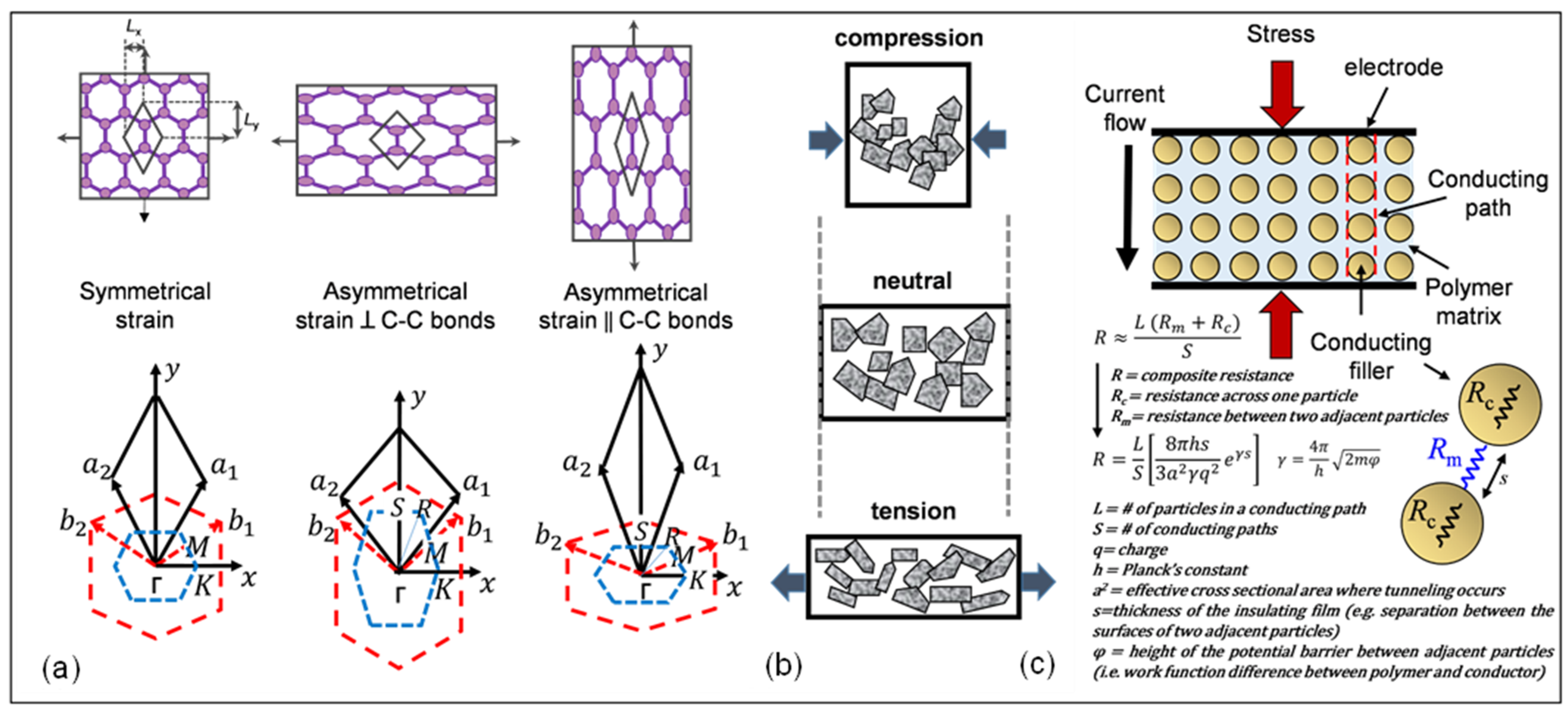
Figure 2.
Overview of the most common techniques to obtain graphene categorized based on top-down and bottom-up processes, along with a tabular comparison on the thickness, lateral size, fundamental advantages and disadvantages of each technique. Reprinted with permission from ref. [74].
Figure 2.
Overview of the most common techniques to obtain graphene categorized based on top-down and bottom-up processes, along with a tabular comparison on the thickness, lateral size, fundamental advantages and disadvantages of each technique. Reprinted with permission from ref. [74].
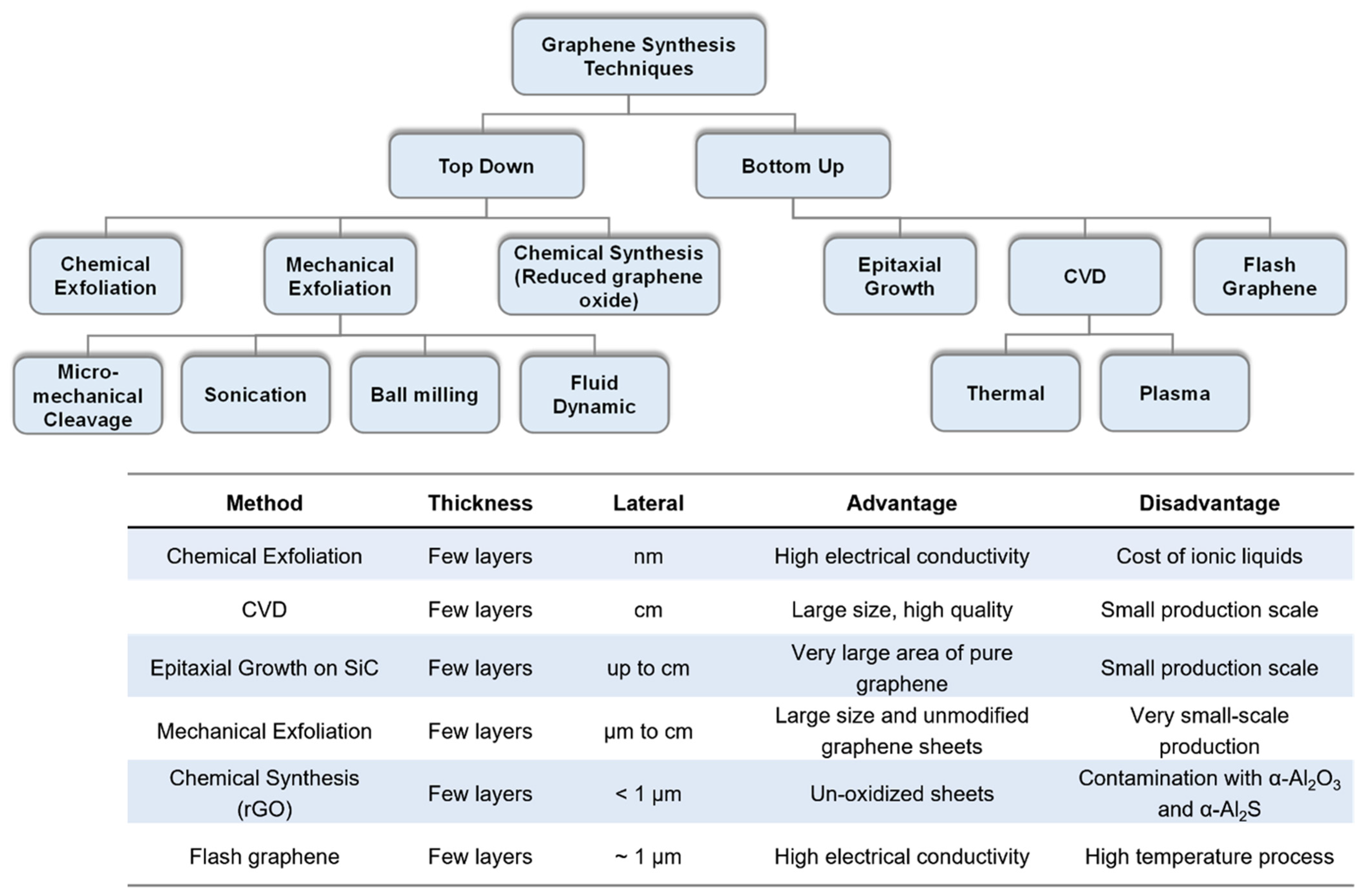
Figure 3.
Methods for synthesizing graphene (a) Schematic of the initial state growth of graphene on copper from ethanol-CVD method. Adapted with permission from ref. [90]. Copyright (2013) American Chemical Society. (b) Schematic illustration of the mechanical exfoliation [92]. (c) An image of graphene flakes on scotch tape [93]. (d) Optical microscopy image of relatively large few layers of transferred graphene flakes on a SiO2/Si. Reprinted from ref. [94], with the permission of AIP Publishing. (e) Schematic diagram of chemical exfoliation by ethanol to form graphene nano plates [95]. (f) The schematic diagram of reducing graphene oxide to develop reduced graphene oxide [96]. (g) Epitaxial growth of graphene on a SiC wafer [97]. (h) Schematic of flash Joule heating (FJH) [79].
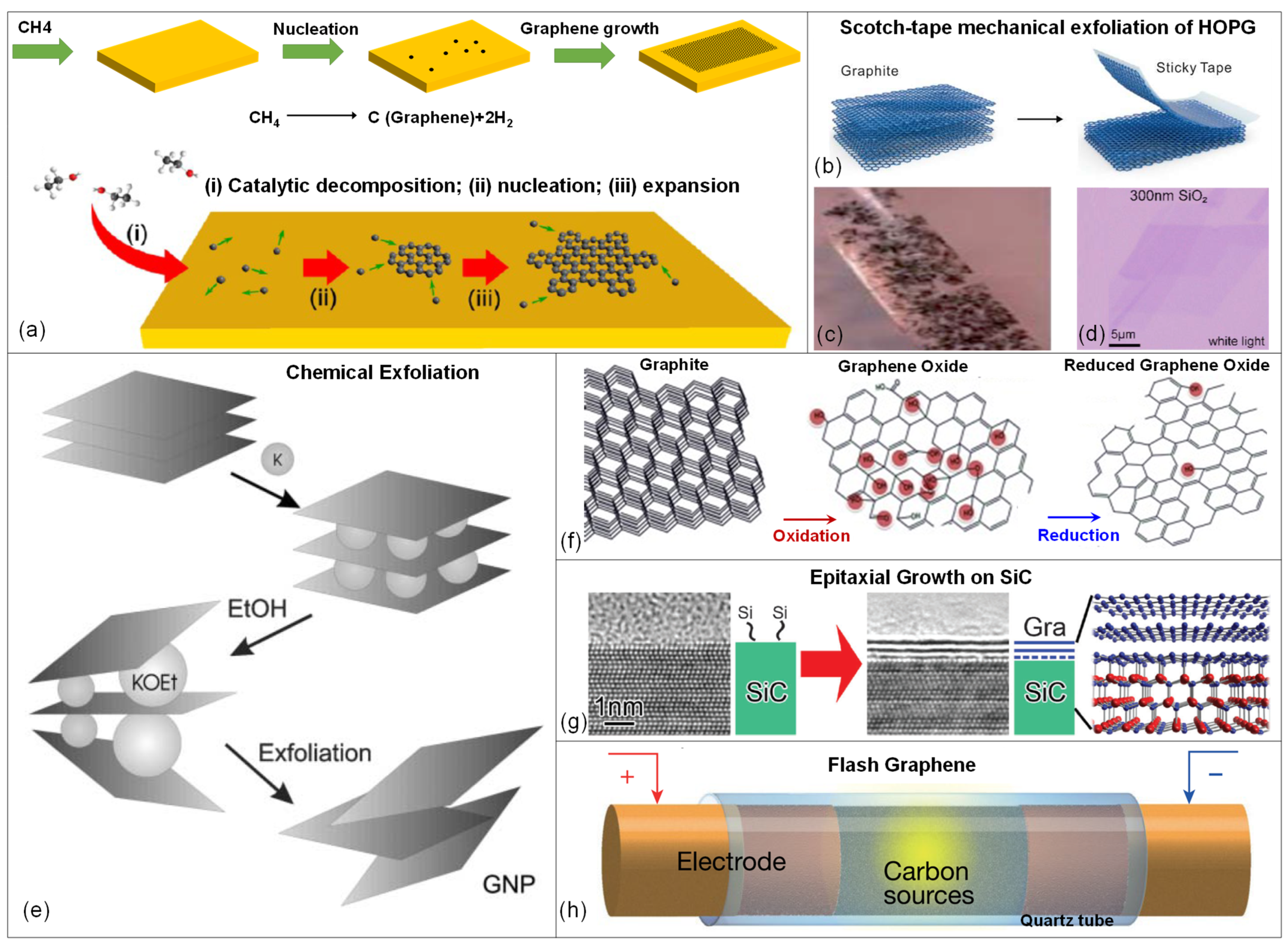
Figure 4.
Dry transfer process for a graphene film grown on a Ni film using a soft substrate, PDMS. (a–c) Schematic illustration of synthesis, etching and transferring processes of graphene films without and with a PDMS stamp. Reprinted with permission from ref. [101]. Copyright (2009) Springer Nature. (d) Using FeCl3 solution to etch underlying Ni layer. Reprinted with permission from ref. [137]. Copyright (2009) Royal Society of Chemistry.(e) Transparent graphene films on the PDMS substrate. Reprinted with permission from ref. [138]. Copyright (2017) Elsevier (f) Optical microscope image of a patterned nickel layer on which graphene is grown and image of the graphene layer on a SiO2 substrate following successful transfer. Adapted with permission from ref. [133]. Copyright (2009) American Chemical Society. (g) A schematic of micropatterned single layer graphene transferring process to a substrate. (h) An optical microscope image of patterned SLG electrode on SiO2. (i) An optical microscope image of patterned SLG electrode on PET/graphene/PVP. Reprinted with permission from ref. [135]. Copyright (2011) John Wiley and Sons.
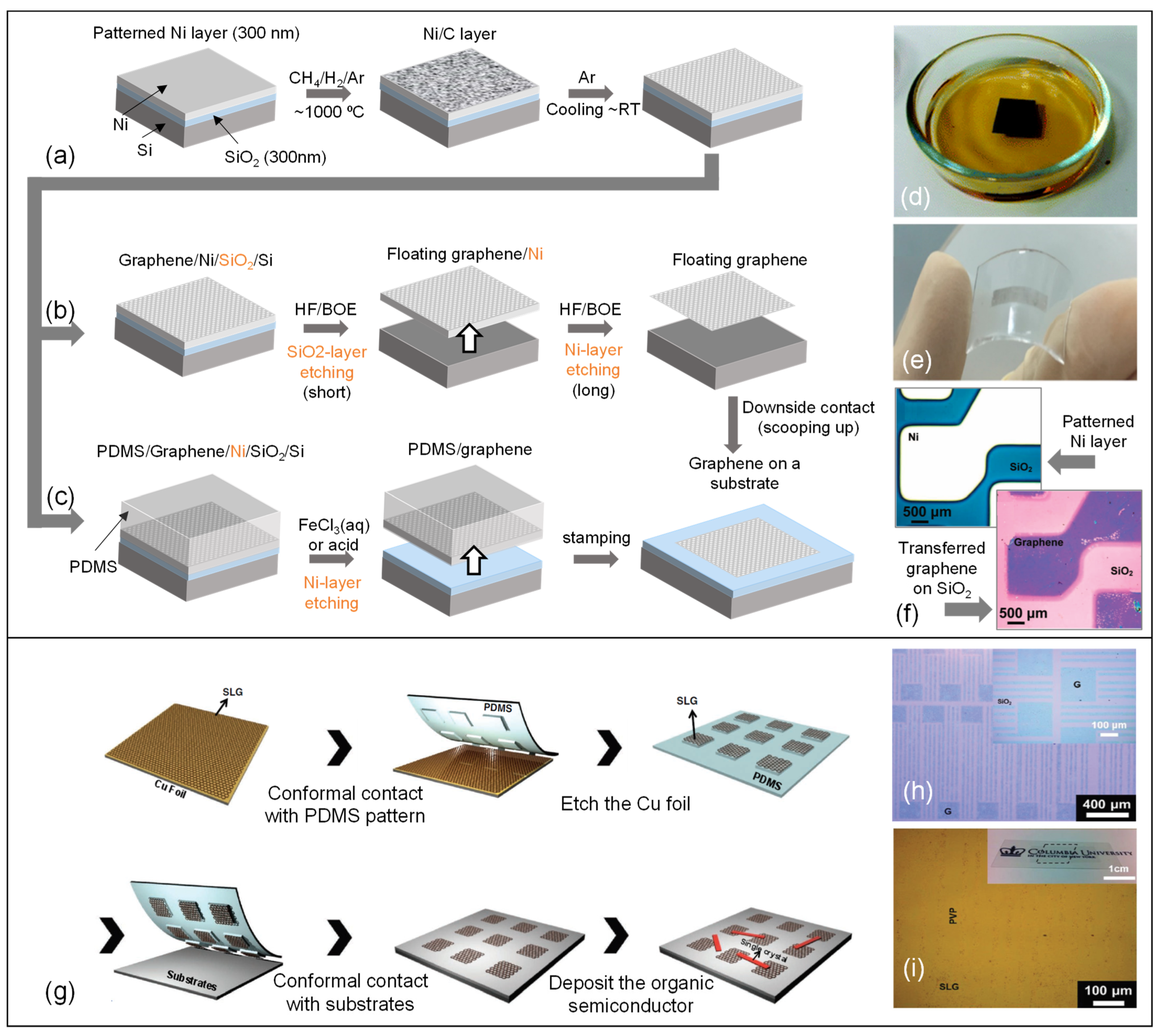
Figure 5.
CVD graphene-based strain gauges: (a) optical microscope images of the as-patterned devices with the zoom-in image of an individual device (arrow marks the bending direction) along with a plot of the resistance change normalized to baseline resistance (ΔR/R0) versus applied strain. Reprinted with permission from ref. [140]. Copyright (2012) AIP Publishing. (b) photograph of transparent graphene strain sensor and variation of resistance with respect to stretching up to 7.1% for graphene strain sensor. Reprinted with permission from ref. [143]. Copyright (2013) Elsevier. (c) photo of “e-skin” with an 8 × 8 device array and resistance change rate with an increase in applied strain. Adapted with permission from ref. [136]. Copyright (2015) American Chemical Society. (d) compression of universal strain sensing and corresponding changes in resistance under different deformation. Reprinted with permission from ref. [144]. Copyright (2012) Elsevier.
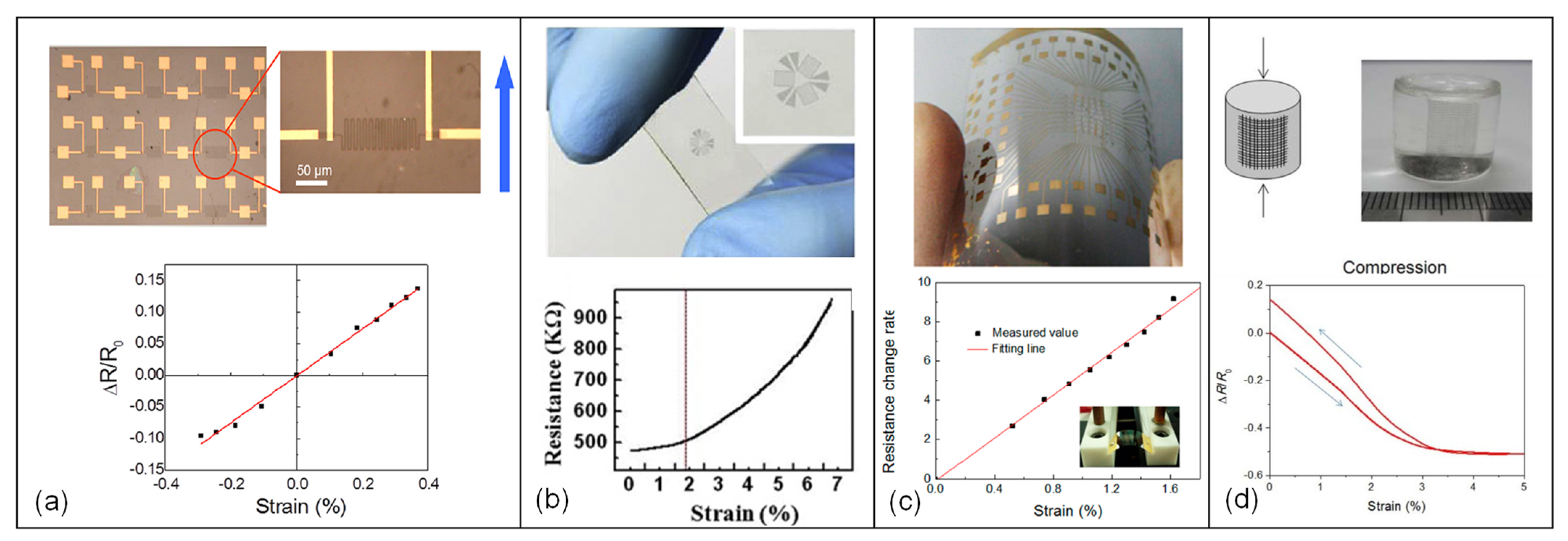
Figure 6.
Exfoliated graphene-based strain gauges (a) Sample of graphene film and curves of normalized change in electrical resistance versus strain for several strain gauges. Adapted with permission from ref. [154]. Copyright (2012) American Chemical Society. (b) SEM image of four suspended graphene devices made from a single flake and the electrical measurements of uniaxially strained graphene (relative change of resistance as function of strain). Adapted with permission from ref. [159]. Copyright (2011) American Chemical Society. (c) Piezoresistive measurement of the fabricated strain sensor on the aluminum specimen, which is under uniaxial tensile loading and relative change in resistance against applied strain [161]. (d) Optical photographs of fabricated GNP/PDMS strain sensor at stretchable, foldable, twistable and demonstration of fabricated GNP strain sensor and relative resistance versus strain [162].
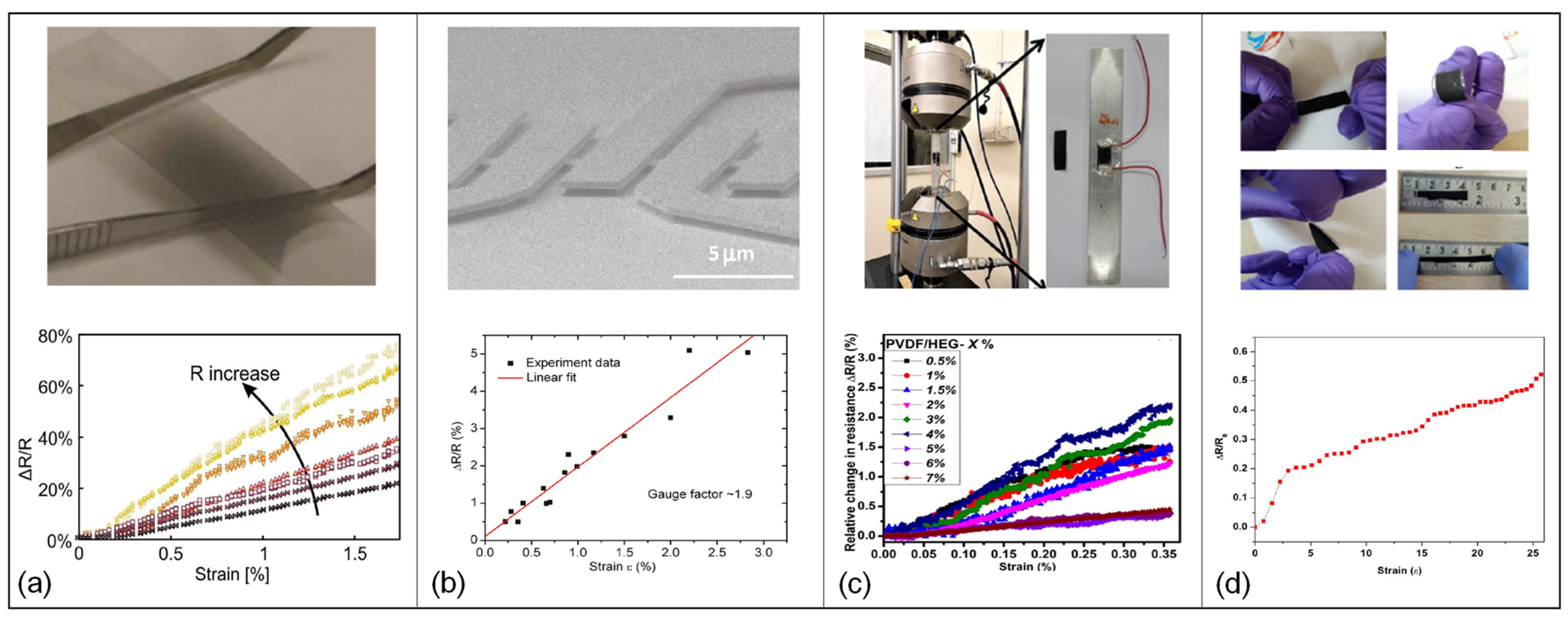
Figure 7.
rGO graphene-based strain gauges: (a) digital photos of arbitrarily bent and twisted strain sensor and the relative resistance changes versus strain curves of the strain sensor under various strains. Adapted with permission from ref. [172]. Copyright (2015) American Chemical Society. (b) photograph of rGO strain sensor and relative resistance-strain curve of a rGO strain sensor recorded at a stretching rate of 10% min−1. Adapted with permission from ref. [177]. Copyright (2016) American Chemical Society. (c) porous rGO membrane on a PET substrate and the relative variation of resistance versus strain for rGO and porous rGO membranes with different membrane porosities, Reprinted with permission from ref. [168]. Copyright (2016) AIP Publishing. (d) SEM images of the cellulose-rGO composites and the relative resistance change, R/R0, as a function of the applied strain. Reprinted with permission from ref. [169]. Copyright (2018) Elsevier.

Figure 8.
(a) Optical microscope image of graphene woven fabrics (GWFs)-PDMS-tape composite film (scale bar 0.1 mm) and the relative resistance change as a function of applied strain varying between 0% and 0.2%. Reprinted with permission from ref. [187]. Copyright (2014) John Wiley and Sons. (b) Photograph of a strain sensor attached to the vibrating membrane of a loudspeaker and to a participants’ throat, where similar change in relative resistance was observed as the same sentence was played from the loudspeaker (black curve) and read out loud (red curve). Reprinted with permission from ref. [189]. Copyright (2015) Springer Nature. (c) Application of graphene nanopaper-based sensors on a glove is imaged and the transitions between the corresponding resistance changes of the strain sensor by the motion of each of the fingers. Reprinted with permission from ref. [173]. Copyright (2013) John Wiley and Sons. (d) Observation of relative resistance changes in the strain sensor on a glove when the finger bends or unbends and using a rosette gauge on the glove to detect the direction of principal strain by applying stretch gently. Reprinted with permission from ref. [143]. Copyright (2013) Elsevier.
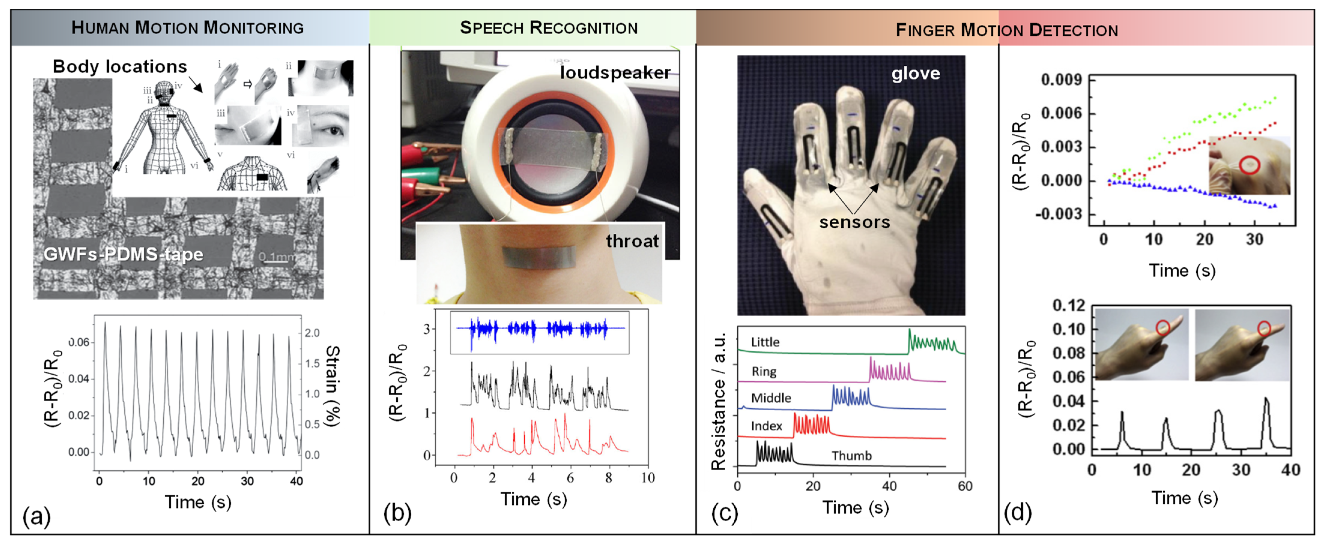
Figure 9.
(a) 3D design of an accelerometer with a suspended graphene ribbons and an attached proof mass [202]. (b) 1-Optical microscope image of graphene piezoresistors on silicon nitride membrane and the schematic of suspended silicon nitride layer under the applied differential pressure. Reprinted with permission from ref. [23]. Copyright (2013) AIP Publishing. (c) Schematic of a suspended graphene cover a circular cavity to measure the chamber pressure due to pressure difference [64].
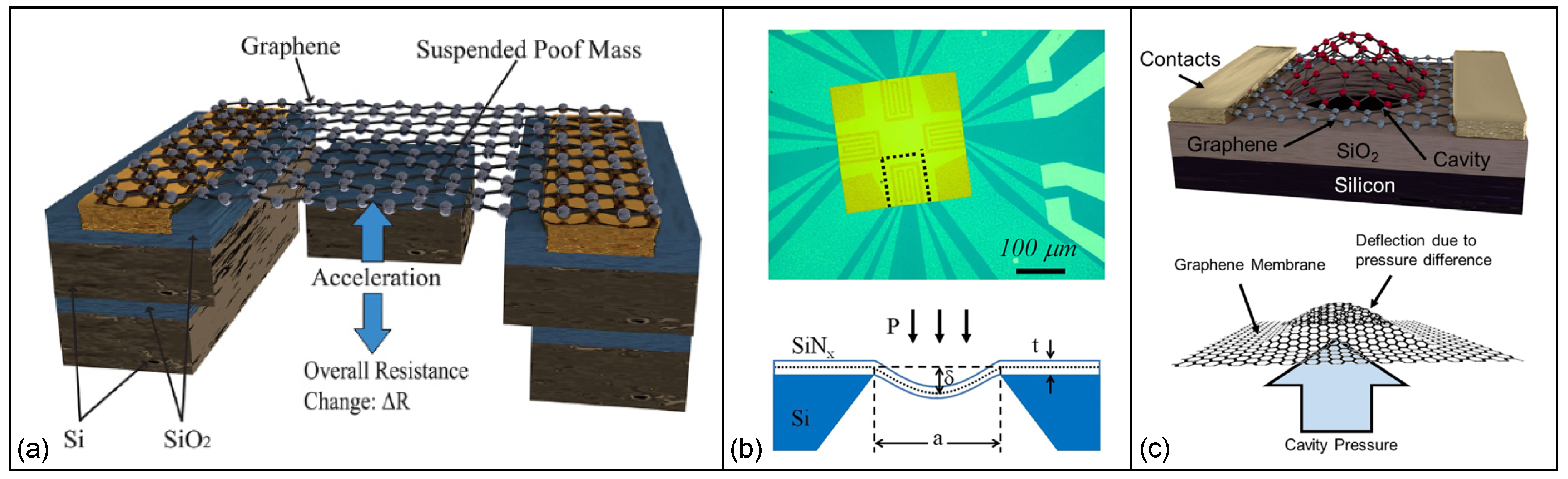

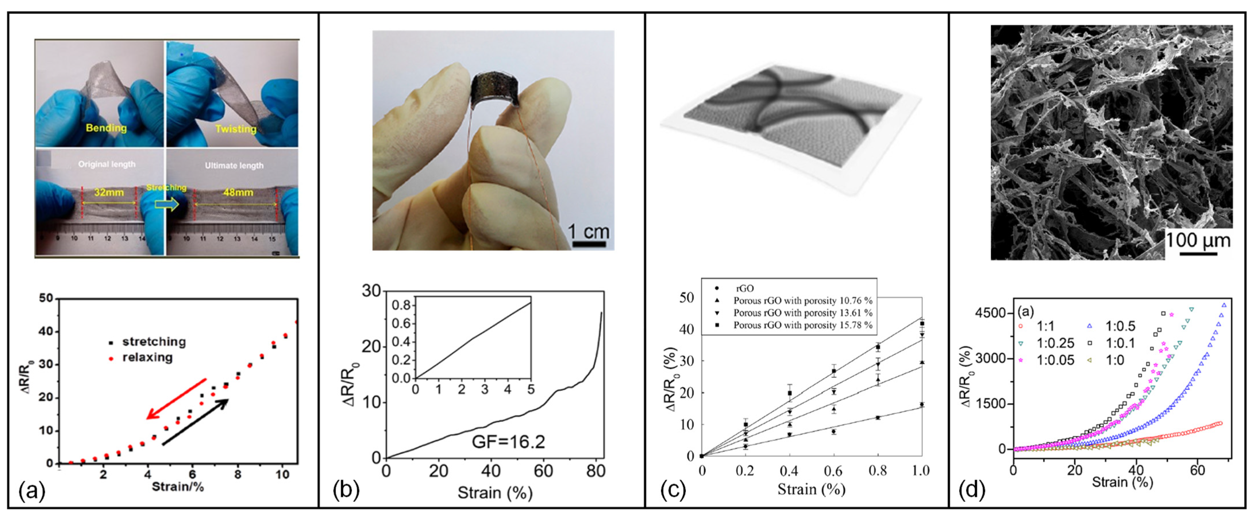
Table 1.
Classification of graphene-based strain gauges in terms of the method used to obtain graphene, along with the device topology and performance metrics like gauge factor and strain range.
Table 1.
Classification of graphene-based strain gauges in terms of the method used to obtain graphene, along with the device topology and performance metrics like gauge factor and strain range.
| Graphene Synthesis Method | Device Topology | Gauge Factor | Strain Range | Ref. |
|---|---|---|---|---|
| CVD | RPECVD graphene on mica substrate | 325 | 0.30% | [140] |
| Graphene-nano graphene sheets on finger | 500 | 1% | [136] | |
| Suspended CVD graphene membrane | 1.6 | 0.25% | [23] | |
| Suspended CVD graphene membrane | 3.67 | 0.29% | [141] | |
| CVD graphene on suspended perforated SiNx membrane | 4.4 | 0.22% | [142] | |
| Graphene glow sensor | 2.4 | 1.8% | [143] | |
| CVD graphene woven fabric on PDMS | 106 | 10% | [144] | |
| Graphene-graphene woven on PDMS | 223 | 3% | [145] | |
| Fragmented graphene foam on PDMS | 15–29 | 77% | [146] | |
| Graphene tactile sensor | 1.4 | - | [147] | |
| CVD graphene on PDMS | 6.1 | 1% | [148] | |
| braided graphene belts sensor | 175.16 | 55% | [149] | |
| planar and crumpled graphene | 20.1 | 105% | [150] | |
| graphene/g-C3N4 heterostructure on PDMS | 1.89 | 25% | [151] | |
| Graphene-single layer graphene on finger | 42.2 | 20% | [26] | |
| Graphene wrapped CNTs | 20 | 1.20% | [152] | |
| PDMS graphene reinforced CNT network | 0.36 | - | [153] | |
| Exfoliated graphene | Spray-deposited graphene on a flexible plastic substrate | 10–100 | 1.70% | [154] |
| Mechanical exfoliated graphene on a silicon wafer | 10–15 | 0.08% | [155] | |
| Mechanical exfoliated graphene nanoribbons | 0.6 | 0.054% | [156] | |
| Mechanical exfoliated graphene nanoribbons | 8.8 | 5% | [157] | |
| Graphene-printed fragments | 125 | 0.30% | [158] | |
| Mechanical exfoliated graphene nanoribbons | 1.9 | 3% | [159] | |
| Graphene solution coated on polypropylene film | 1000 | 0.05–0.265% | [160] | |
| Polymer-functionalized hydrogen-exfoliated graphene | 10 | 0.35% | [161] | |
| Graphene nanoplatelet on PDMS | 62.5 | 2.5–25% | [162] | |
| PDMS-graphene nanoplatelet/CNT hybrids | 1000 | 18% | [163] | |
| Carbon nanotube-graphene nanoplatelet hybrid film | <1 | - | [164] | |
| rGO | Mechanical exfoliated Graphene ripple on PDMS | −2 | 20% | [165] |
| 3D graphene foam-PDMS nanocomposite | 178 | 30% | [166] | |
| rGO on a PET substrate | 61.5 | 0.01–0.04% | [167] | |
| rGO membrane porous structure | 15.2–46.1 | 1% | [168] | |
| PDMS-cellulose-rGO/CNFs hybrids | 9.4 | 70% | [169] | |
| 3D porous PDMS CNT/rGO hybrid | 1.6 | 80% | [170] | |
| Polyurethane-silver nanowires/graphene hybrids | 20–400 | 0.3–1% | [171] | |
| rGO-microtube on PDMS | 630 | 50% | [172] | |
| Crumpled graphene-nanocellulose composite on elastomer matrix | −7.1 | 100% | [173] | |
| rGO doped with polystyrene nanoparticles (PS) on PDMS | 250 | 1.05% | [174] | |
| Polymerized rGO on TPU | 23.15–6583 | 550% | [175] | |
| rGO mesh on an LCP substrate | 375–473 | 0.1–1.4% | [176] | |
| rGO-fish scale like on an elastic tape | 16 | 82% | [177] | |
| rGO-conductive cotton fabric | - | 0.02–0.35% | [178] | |
| rGO-FET on polyethersulfone (PES) | 20 | 50% | [179] |
Publisher’s Note: MDPI stays neutral with regard to jurisdictional claims in published maps and institutional affiliations. |
© 2022 by the authors. Licensee MDPI, Basel, Switzerland. This article is an open access article distributed under the terms and conditions of the Creative Commons Attribution (CC BY) license (https://creativecommons.org/licenses/by/4.0/).
Share and Cite
MDPI and ACS Style
Irani, F.S.; Shafaghi, A.H.; Tasdelen, M.C.; Delipinar, T.; Kaya, C.E.; Yapici, G.G.; Yapici, M.K. Graphene as a Piezoresistive Material in Strain Sensing Applications. Micromachines 2022, 13, 119. https://doi.org/10.3390/mi13010119
AMA Style
Irani FS, Shafaghi AH, Tasdelen MC, Delipinar T, Kaya CE, Yapici GG, Yapici MK. Graphene as a Piezoresistive Material in Strain Sensing Applications. Micromachines. 2022; 13(1):119. https://doi.org/10.3390/mi13010119
Chicago/Turabian StyleIrani, Farid Sayar, Ali Hosseinpour Shafaghi, Melih Can Tasdelen, Tugce Delipinar, Ceyda Elcin Kaya, Guney Guven Yapici, and Murat Kaya Yapici. 2022. "Graphene as a Piezoresistive Material in Strain Sensing Applications" Micromachines 13, no. 1: 119. https://doi.org/10.3390/mi13010119
Note that from the first issue of 2016, this journal uses article numbers instead of page numbers. See further details here.