
Progress in Avalanche Photodiodes for Laser Ranging


Abstract
1. Introduction
2. Laser Ranging
2.1. Impulse Time-of-Flight Ranging Method
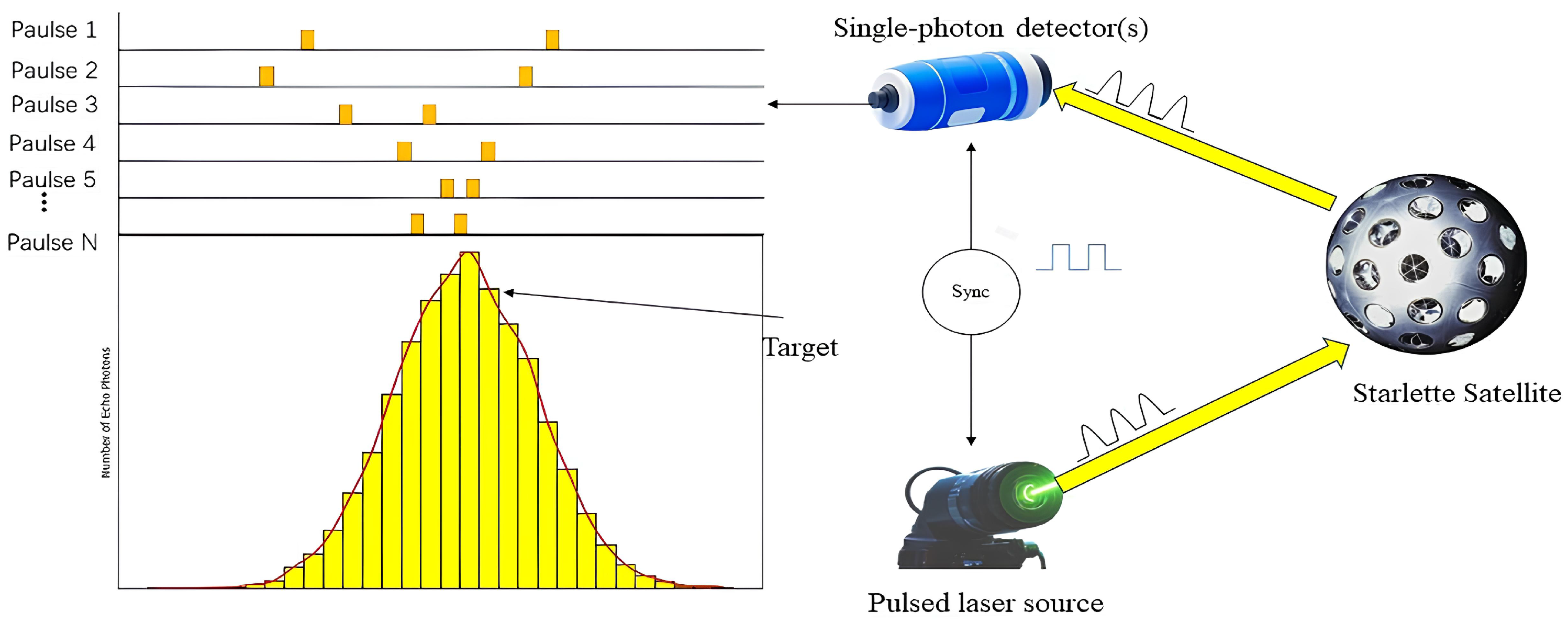
2.2. Time-Correlated Photon-Counting Method
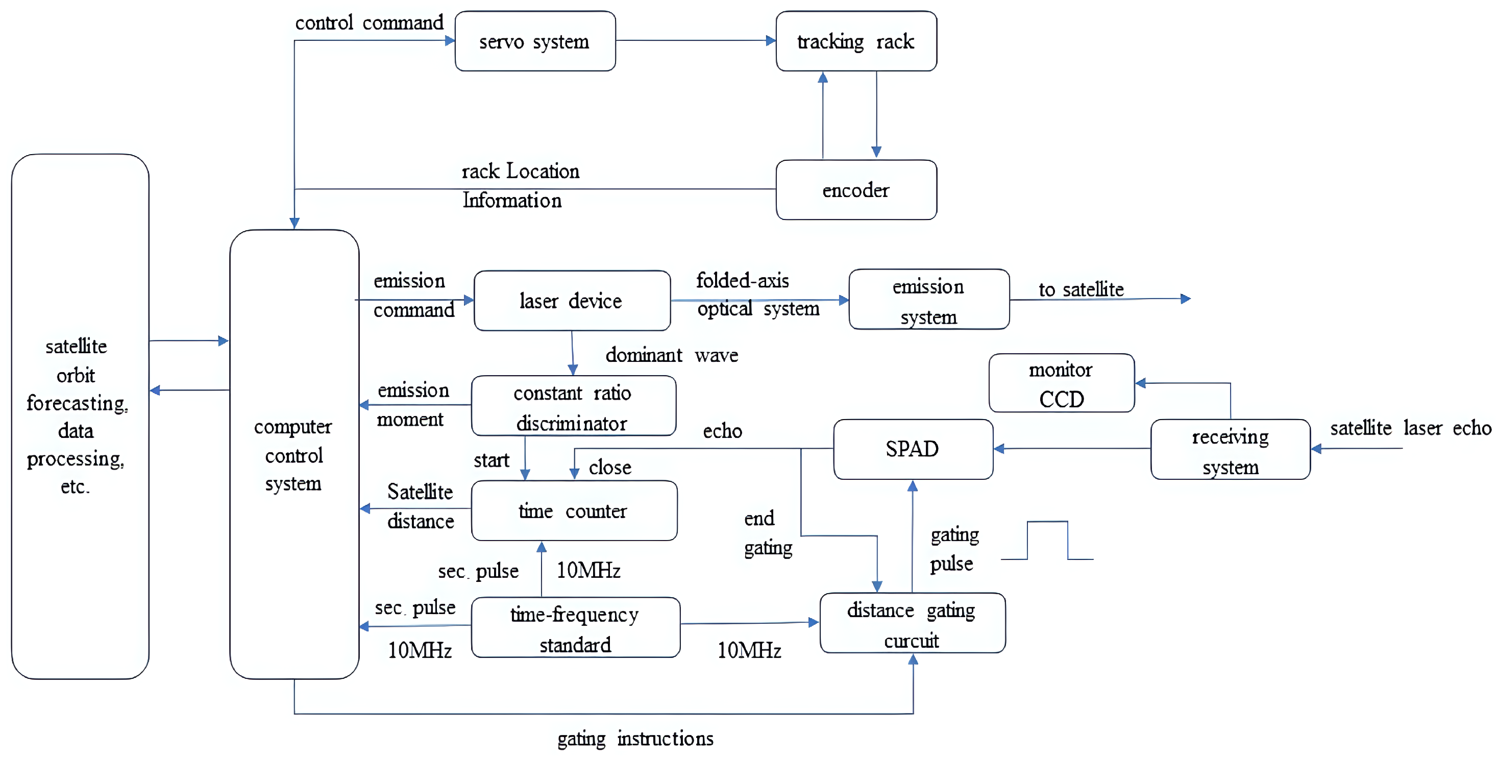
2.3. Laser Ranging System
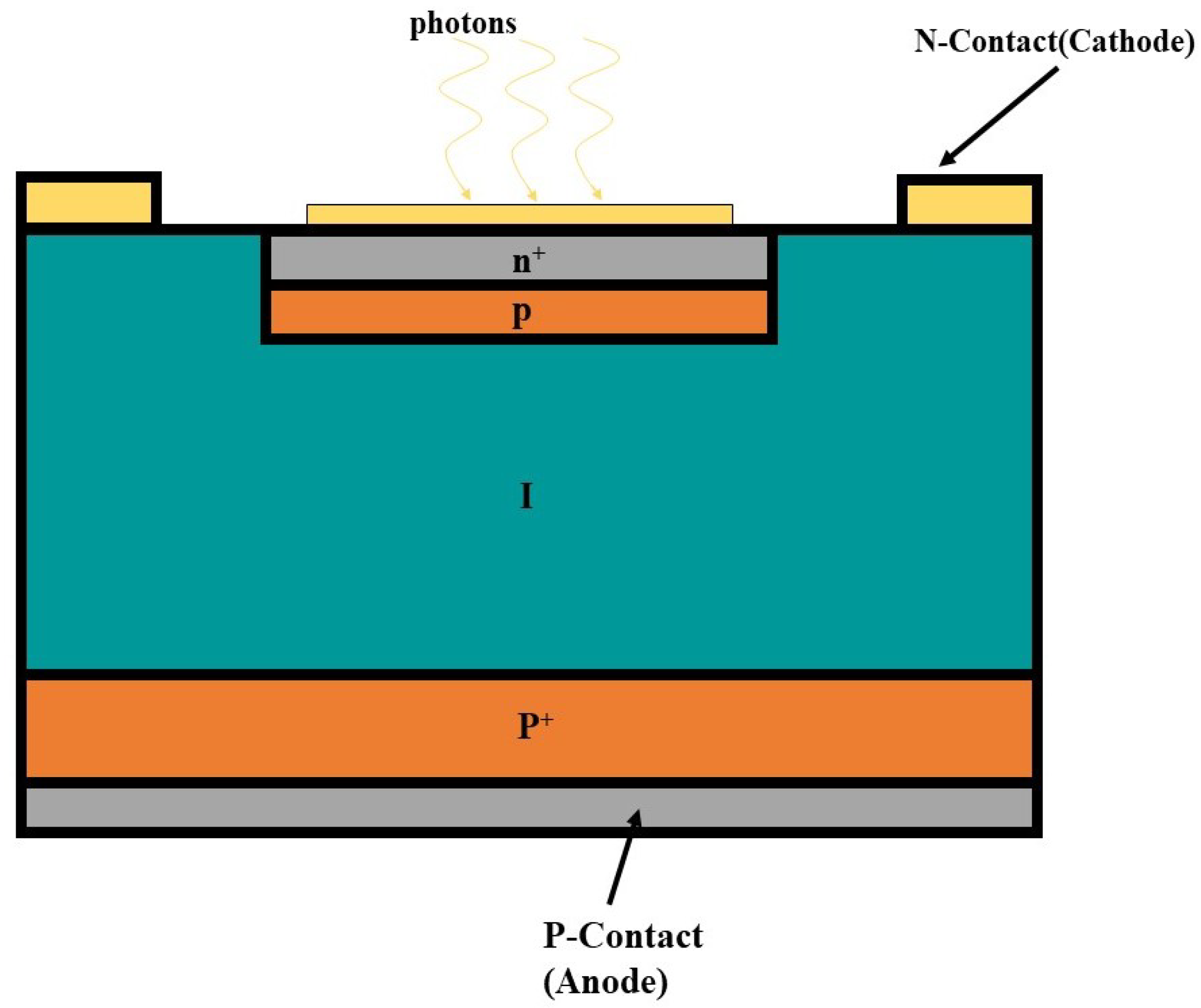
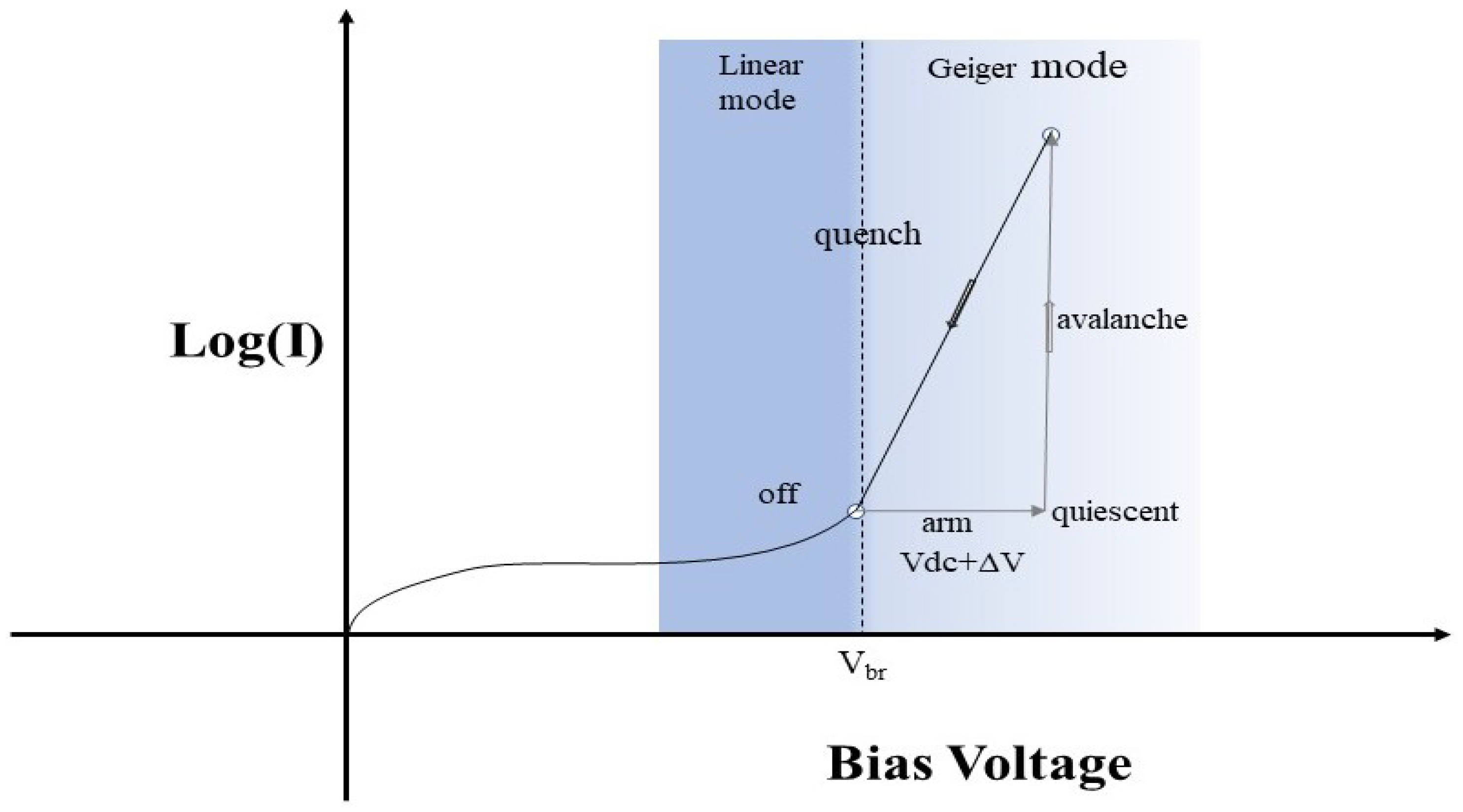
3. Avalanche Photodiode
3.1. Si-APD Research Progress and Application
3.2. InGaAs/InP APD Research Progress and Applications
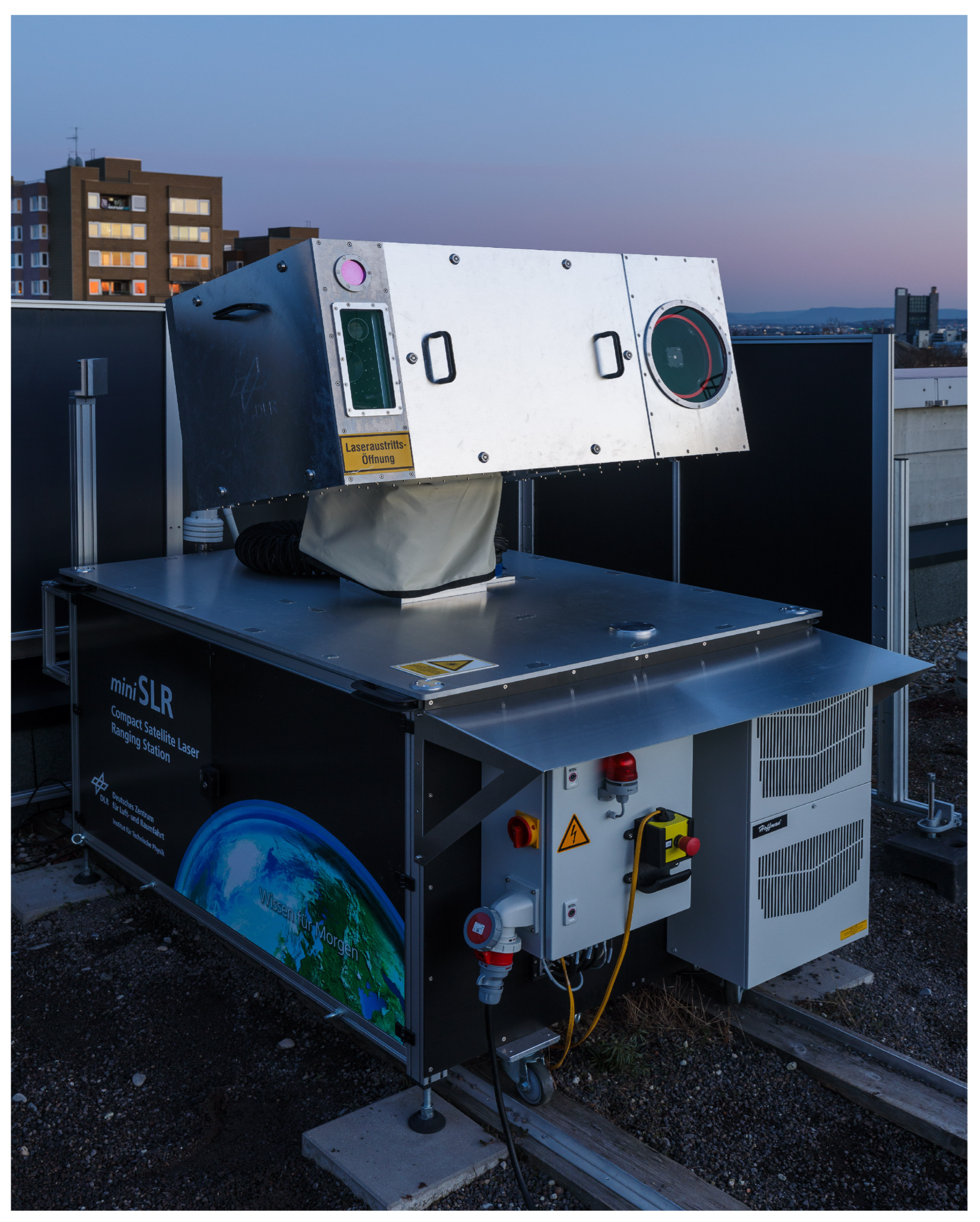
3.3. Avalanche Photodiodes in Mini SLR Systems
4. Trends in Laser Ranging Avalanche Photodiode Research
5. Conclusions
Author Contributions
Funding
Conflicts of Interest
Abbreviations
| SLR | Satellite Laser Ranging |
| DLR | Debris Laser Ranging |
| LLR | Lunar Laser Ranging |
| LEO | Low Earth Orbit |
| GEO | Geosynchronous Orbit |
| TOF | Time Of Flight |
| PMT | Photomultiplier |
| APD | Avalanche Photon Diode |
| SPAD | Single-Photon Avalanche Diode |
| SNSPD | Superconducting Nanowire Single-Photon Detector |
| TCSPC | Time-Correlated Single-Photon Counting |
| SAGCM | Separate Absorption Grading Charge Multiplication |
| FGR | Floating Guard Ring |
| DCR | Dark Count Rate |
| PDE | Photon-Detection Efficiency |
| FWHM | Full Width at Half Maximum |
| MBE | Molecular Beam Epitaxy |
| MOCVD | Metal–Organic Chemical Vapour Deposition |
| FPGAs | Field-Programmable Gate Arrays |
| PQAR | Passive Quenching Active Reset |
| PQPR | Passive Quenching Passive Reset |
| PQACR | Passive Quenching Active Clock-Driven Reset |
References
- Urschl, C.; Beutler, G.; Gurtner, W.; Hugentobler, U.; Schaer, S. Contribution of SLR tracking data to GNSS orbit determination. Adv. Space Res. 2007, 39, 1515–1523. [Google Scholar] [CrossRef]
- Tapley, B.D.; Schutz, B.E.; Eanes, R.J. Satellite Laser Ranging and its Applications. In Fundamental Astronomy and Solar System Dynamics: Invited Papers Honoring Prof. Walter Fricke on the Occasion of His 70th Birthday; Duncombe, R.L., Lieske, J.H., Seidelmann, P.K., Eds.; Springer: Dordrecht, The Netherlands, 1986; pp. 247–261. [Google Scholar] [CrossRef]
- McGarry, J.; Hoffman, E.; Degnan, J.; Cheek, J.; Clarke, C.; Diegel, I.; Donovan, H.; Horvath, J.; Marzouk, M.; Nelson, A.; et al. NASA’s satellite laser ranging systems for the twenty-first century. J. Geod. 2019, 93, 2249–2262. [Google Scholar] [CrossRef] [PubMed]
- Zhou, H.; Chen, Y.; Hyyppä, J.; Li, S. An overview of the laser ranging method of space laser altimeter. Infrared Phys. Technol. 2017, 86, 147–158. [Google Scholar] [CrossRef]
- Zappa, F.; Ripamonti, G.; Lacaita, A.; Cova, S.; Samori, C. Tracking capabilities of SPADs for laser ranging. In Proceedings of the Eighth International Workshop on Laser Ranging Instrumentation, Annapolis, MD, USA, 18–22 May 1992; NASA. Goddard Space Flight Center: Greenbelt, MD, USA, 1993. [Google Scholar]
- Hu, X.; Cheng, Y.; Gu, C.; Zhu, X.; Liu, H. Superconducting nanowire single-photon detectors: Recent progress. Sci. Bull. 2015, 60, 1980–1983. [Google Scholar] [CrossRef]
- Richards, P.L. Bolometers for infrared and millimeter waves. J. Appl. Phys. 1994, 76, 1–24. [Google Scholar] [CrossRef]
- Guo, N.; Gao, C.; Xue, M.; Niu, L.; Zhu, S.; Feng, L.; He, H.; Cao, Z. Ranging method based on linear frequency modulated laser. Laser Phys. 2017, 27, 065108. [Google Scholar] [CrossRef]
- Tao, M.; Gong, X.; Hou, Y.; Li, B.; Song, J.; Chen, J.; Gao, F. Time-of-flight ranging method by measuring pulse laser phase based on field-programmable gate array digital mixing. Meas. Sci. Technol. 2020, 32, 025004. [Google Scholar] [CrossRef]
- Wang, K.; Wen, Z.; Guo, W.; Xiong, Y.; Yang, L.; Wang, P. Amplitude modulation ranging achieved by self-sweeping fiber laser in a short distance. Infrared Phys. Technol. 2023, 134, 104895. [Google Scholar] [CrossRef]
- Dequal, D.; Agnesi, C.; Sarrocco, D.; Calderaro, L.; Bianco, G. 100 kHz satellite laser ranging demonstration at Matera Laser Ranging Observatory. J. Geod. 2021, 95, 26. [Google Scholar] [CrossRef]
- Haitz, R.H. Model for the Electrical Behavior of a Microplasma. J. Appl. Phys. 1964, 35, 1370–1376. [Google Scholar] [CrossRef]
- McIntyre, R.J. Theory of Microplasma Instability in Silicon. J. Appl. Phys. 1961, 32, 983–995. [Google Scholar] [CrossRef]
- Leonard, D.; Krishnamurthy, M.; Reaves, C.M.; Denbaars, S.P.; Petroff, P.M. Direct formation of quantum-sized dots from uniform coherent islands of InGaAs on GaAs surfaces. Appl. Phys. Lett. 1993, 63, 3203–3205. [Google Scholar] [CrossRef]
- Levine, B.F.; Bethea, C.G.; Hasnain, G.; Walker, J.; Malik, R.J. High-detectivity D* = 1.0 × 1010 cm √/W GaAs/AlGaAs multiquantum well lambda = 8.3 upmum infrared detector. Appl. Phys. Lett. 1988, 53, 296–298. [Google Scholar] [CrossRef]
- Phillips, J.; Kamath, K.; Bhattacharya, P. Far-infrared photoconductivity in self-organized InAs quantum dots. Appl. Phys. Lett. 1998, 72, 2020–2022. [Google Scholar] [CrossRef]
- Rowe, M.A.; Gansen, E.J.; Greene, M.; Hadfield, R.H.; Harvey, T.E.; Su, M.Y.; Nam, S.W.; Mirin, R.P.; Rosenberg, D. Single-photon detection using a quantum dot optically gated field-effect transistor with high internal quantum efficiency. Appl. Phys. Lett. 2006, 89, 253505. [Google Scholar] [CrossRef]
- Maruyama, T.; Narusawa, F.; Makoto, K.; Tanaka, M.; Saito, Y.; Nomura, A. Development of a near-infrared photon-counting system using an InGaAs avalanche photodiode. Opt. Eng. 2002, 41, 395–402. [Google Scholar] [CrossRef]
- Bowman, S.R.; Shih, Y.H.; Alley, C.O.; Cruickshank, J.M.; Harney, R.C. The use of Geiger mode avalanche photodiodes for precise laser ranging at very low light levels—An experimental evaluation. Int. Soc. Opt. Photonics 1986, 0663, 24–29. [Google Scholar]
- Prochazka, I.; Hamal, K.; Sopko, B. Recent achievements in single photon detectors and their applications. Opt. Acta Int. J. Opt. 2004, 51, 1289–1313. [Google Scholar] [CrossRef]
- Azka, I.P.; Hamal, K.; Sopko, B. Photodiode based detector package for centimeter satellite ranging. In Proceedings of the 7th International Workshop on Laser Ranging Instrumentation, Matera, Italy, 2–6 October 1989. [Google Scholar]
- Proch, I. The solid state detector technology for picosecond laser ranging. In Proceedings of the Eighth International Workshop on Laser Ranging Instrumentation, Annapolis, MD, USA, 18–22 May 1992; NASA. Goddard Space Flight Center: Greenbelt, MD, USA, 1993. [Google Scholar]
- Kirchner, G.; Koidl, F.; Blazej, J.; Hamal, K.; Prochazka, I. Time-walk-compensated SPAD: Multiple-photon versus single-photon operation. In Proceedings of the Aerospace Remote Sensing, London, UK, 22 December 1997. [Google Scholar]
- Kirchner, G.; Koidl, F. Compensation of SPAD time-walk effects. J. Opt. A Pure Appl. Opt. 1999, 1, 163. [Google Scholar] [CrossRef]
- Kirchner, G.; Koidl, F.; Azka, I.P.; Hamal, K. SPAD time Walk Compensation and Return Energy Dependent Ranging. In Proceedings of the 11th International Workshop on Laser Ranging, Deggendorf, Germany, 21–25 September 1998. [Google Scholar]
- Prochazka, I.; Kral, L.; Hamal, K.; Sopko, B. Photon counting timing uniformity–unique feature of the silicon avalanche photodiodes K14. J. Mod. Opt. 2007, 54, 141–149. [Google Scholar] [CrossRef]
- Vojtěch, M.; Ivan, P.; Josef, B. Twenty Years of Rad-Hard K14 SPAD in Space Projects. Sensors 2015, 15, 18178–18196. [Google Scholar] [CrossRef]
- Prochazka, I.; Kodet, J.; Eckl, J.; Blazej, J. Note: Large active area solid state photon counter with 20 ps timing resolution and 60 fs detection delay stability. Rev. Sci. Instrum. 2017, 88, 106105. [Google Scholar] [CrossRef]
- Prochazka, I.; Blazej, J.; Flekova, T.; Kodet, J. Silicon Based Photon Counting Detector Providing Femtosecond Detection Delay Stability; Institute of Electrical and Electronics Engineers (IEEE): Piscataway, NJ, USA, 2020. [Google Scholar]
- Prochazka, I.; Bimbovar, R.; Blazej, J.; Kodet, J. Recent progress in SPAD detectors for SLR and laser time transfer. In Proceedings of the 22nd ILRS Workshop: Reconnecting the ILRS Community, Guadalajara, Spain, 7–11 November 2022. [Google Scholar]
- Giudice, A.; Simmerle, G.; Veronese, D.; Biasi, R.; Maccagnani, P. High-detection efficiency and picosecond timing compact detector modules with red-enhanced SPADs. In Advanced Photon Counting Techniques VI; SPIE: Bellingham, WA, USA, 2012. [Google Scholar]
- Zhang, H.-Y.; Wang, L.-L.; Wu, C.-Y.; Wang, Y.-R.; Yang, L.; Pan, H.-F.; Liu, Q.-L.; Guo, X.; Tang, K.; Zhang, Z.-P.; et al. Avalanche photodiode single-photon detector with high time stability. Acta Phys. Sin. 2020, 69, 20191875. [Google Scholar] [CrossRef]
- Pearsall, T.P.; Dipda, E.; Papuchon, M.; Roullet, G. A High Performance Avalanche Photodiode at 1.0–1.7 μm, Compatible with InP/GaxIn1—xAsyP1—y Integrated Optics Technology. In Proceedings of the Integrated and Guided Wave Optics, Salt Lake City, UT, USA, 16–18 January 1978; Optica Publishing Group: Washington, DC, USA, 1978; p. MC2. [Google Scholar] [CrossRef]
- Nishida, K.; Taguchi, K.; Matsumoto, Y. InGaAsP heterostructure avalanche photodiodes with high avalanche gain. Appl. Phys. Lett. 1979, 35, 251–253. [Google Scholar] [CrossRef]
- Ma, C.; Deen, M.; Tarof, L. Multiplication in separate absorption, grading, charge, and multiplication InP-InGaAs avalanche photodiodes. IEEE J. Quantum Electron. 1995, 31, 2078–2089. [Google Scholar] [CrossRef]
- Kao, Y.; Wolley, E. High-voltage planar p-n junctions. Proc. IEEE 1967, 55, 1409–1414. [Google Scholar] [CrossRef]
- Levine, B.F.; Bethea, C.G.; Campbell, J.C. Room-temperature 1.3-μm optical time domain reflectometer using a photon counting InGaAs/InP avalanche detector. Appl. Phys. Lett. 1985, 46, 333–335. [Google Scholar] [CrossRef]
- Lacaita, A.; Francese, P.A.; Zappa, F.; Cova, S. Single-photon detection beyond 1 μm: Performance of commercially available germanium photodiodes. Appl. Opt. 1994, 33, 6902–6918. [Google Scholar] [CrossRef]
- McIntosh, K.A.; Donnelly, J.P.; Oakley, D.C.; Napoleone, A.; Calawa, S.D.; Mahoney, L.J.; Molvar, K.M.; Duerr, E.K.; Groves, S.H.; Shaver, D.C. InGaAsP/InP avalanche photodiodes for photon counting at 1.06 μm. Appl. Phys. Lett. 2002, 81, 2505–2507. [Google Scholar] [CrossRef]
- Donnelly, J.; Duerr, E.; Mcintosh, K.; Dauler, E.; Oakley, D.; Groves, S.; Vineis, C.; Mahoney, L.; Molvar, K.; Hopman, P.; et al. Design Considerations for 1.06-mum InGaAsP–InP Geiger-Mode Avalanche Photodiodes. IEEE J. Quantum Electron. 2006, 42, 797–809. [Google Scholar] [CrossRef]
- Itzler, M.A.; Jiang, X.; Ben-Michael, R.; Slomkowski, K.; Krainak, M.A.; Wu, S.; Sun, X. InGaAsP/InP single photon avalanche photodetectors for 1.06 μm free-running photon counting. In Proceedings of the 2007 Conference on Lasers and Electro-Optics (CLEO), Baltimore, MD, USA, 6–11 May 2007; pp. 1–2. [Google Scholar] [CrossRef]
- Jiang, X.; Itzler, M.A.; Ben-Michael, R.; Slomkowski, K. InGaAsP–InP Avalanche Photodiodes for Single Photon Detection. IEEE J. Sel. Top. Quantum Electron. 2007, 13, 895–905. [Google Scholar] [CrossRef]
- Verghese, S.; Donnelly, J.P.; Duerr, E.K.; McIntosh, K.A.; Chapman, D.C.; Vineis, C.J.; Smith, G.M.; Funk, J.E.; Jensen, K.E.; Hopman, P.I.; et al. Arrays of InP-based Avalanche Photodiodes for Photon Counting. IEEE J. Sel. Top. Quantum Electron. 2007, 13, 870–886. [Google Scholar] [CrossRef]
- Ramirez, D.A.; Hayat, M.M.; Itzler, M.A. Dependence of the Performance of Single Photon Avalanche Diodes on the Multiplication Region Width. IEEE J. Quantum Electron. 2008, 44, 1188–1195. [Google Scholar] [CrossRef]
- Itzler, M.A.; Jiang, X.; Entwistle, M.; Slomkowski, K.; Tosi, A.; Acerbi, F.; Zappa, F.; Cova, S. Advances in InGaAsP-based avalanche diode single photon detectors. J. Mod. Opt. 2011, 58, 174–200. [Google Scholar] [CrossRef]
- Jiang, X.; Itzler, M.A.; Ben-Michael, R.; Slomkowski, K.; Sun, X. Afterpulsing Effects in Free-Running InGaAsP Single-Photon Avalanche Diodes. IEEE J. Quantum Electron. 2008, 44, 3–11. [Google Scholar] [CrossRef]
- Buller, G.S.; Krichel, N.J.; McCarthy, A.; Gemmell, N.R.; Tanner, M.G.; Natarajan, C.M.; Ren, X.; Hadfield, R.H. Kilometer range depth imaging using time-correlated single-photon counting. In Infrared Sensors, Devices, and Applications; and Single Photon Imaging II; SPIE: Bellingham, WA, USA, 2011; Volume 8155, pp. 457–464. [Google Scholar]
- Xue, L.; Zhang, L.; Zhang, S.; Li, M.; Kang, L.; Chen, J.; Wu, P. Satellite laser ranging using superconducting nanowire single-photon detectors at 1064nm wavelength. Opt. Lett. 2016, 41, 3848. [Google Scholar] [CrossRef] [PubMed]
- Pawlikowska, A.M.; Halimi, A.; Lamb, R.A.; Buller, G.S. Single-photon three-dimensional imaging at up to 10 kilometers range. Opt. Express 2017, 25, 11919. [Google Scholar] [CrossRef]
- Li, Z.P.; Ye, J.T.; Huang, X.; Jiang, P.Y.; Cao, Y.; Hong, Y.; Yu, C.; Zhang, J.; Zhang, Q.; Peng, C.Z.; et al. Single-photon imaging over 200 km. Optica 2021, 8, 344–349. [Google Scholar] [CrossRef]
- Shen, G.; Zheng, T.; Li, Z.; Yang, L.; Wu, G. Self-gating single-photon time-of-flight depth imaging with multiple repetition rates. Opt. Lasers Eng. 2022, 151, 106908. [Google Scholar] [CrossRef]
- Bimbová, R.; Procházka, I.; Kodet, J.; Blažej, J. Photon counting detectors based on InGaAs/InP for space objects laser ranging. IEEE J. Sel. Top. Quantum Electron. 2021, 28, 3802605. [Google Scholar] [CrossRef]
- Miao, Y.; Lin, H.; Li, B.; Dong, T.; He, C.; Du, J.; Zhao, X.; Zhou, Z.; Su, J.; Wang, H.; et al. Review of Ge (GeSn) and InGaAs avalanche diodes operating in the SWIR spectral region. Nanomaterials 2023, 13, 606. [Google Scholar] [CrossRef] [PubMed]
- Vines, P.; Kuzmenko, K.; Kirdoda, J.; Dumas, D.C.; Mirza, M.M.; Millar, R.W.; Paul, D.J.; Buller, G.S. High performance planar germanium-on-silicon single-photon avalanche diode detectors. Nat. Commun. 2019, 10, 1086. [Google Scholar] [CrossRef] [PubMed]
- Hampf, D.; Niebler, F.; Meyer, T.; Riede, W. The miniSLR: A low-budget, high-performance satellite laser ranging ground station. J. Geod. 2024, 98, 8. [Google Scholar] [CrossRef]
- Ren, X.; Fan, Y.; Shi, Y.; Yuan, Z.; Huang, Y.; Zhang, W. Hybrid Integration of Single-Photon Avalanche Diode Array and Silicon Photonic Chip. Acta Opt. Sin. (Online) 2024, 1, 0104001. [Google Scholar]
- Huang, H.H.; Liu, C.H.; Huang, T.Y.; Lin, S.D.; Lee, C.Y. Self-restoring and low-jitter circuits for high timing-resolution SPAD sensing applications. In Proceedings of the 2023 IEEE International Symposium on Circuits and Systems (ISCAS), Monterey, CA, USA, 21–25 May 2023; IEEE: Piscataway, NJ, USA, 2023; pp. 1–5. [Google Scholar]


| Target Satellite | Laser Type and Wavelength (nm) | Detector Type and Applicable Wavelength (nm) | Mean Time of Light (s) | Perigee Altitude (km) | Zenith Angle (°) | Return Photon Number |
|---|---|---|---|---|---|---|
| ajisai | Nd-Yag@1064 | CSPAD@532 | 0.017116485598 | 1479 | 54.82660396144291 | 118.9024 |
| lageos-2 | Nd-Yag@1064 | CSPAD@532 | 0.041059333398 | 5617 | 24.21489660834258 | 3.5909 |
| etalon-2 | Nd-Yag@1064 | CSPAD@532 | 0.132175862032 | 19097 | 15.58953384198299 | 0.033438 |
| beidou3m-1 | Nd-Yag@1064 | CSPAD@532 | 0.147367634768 | 21519 | 13.22384987727686 | 0.021639 |
Disclaimer/Publisher’s Note: The statements, opinions and data contained in all publications are solely those of the individual author(s) and contributor(s) and not of MDPI and/or the editor(s). MDPI and/or the editor(s) disclaim responsibility for any injury to people or property resulting from any ideas, methods, instructions or products referred to in the content. |
© 2025 by the authors. Licensee MDPI, Basel, Switzerland. This article is an open access article distributed under the terms and conditions of the Creative Commons Attribution (CC BY) license (https://creativecommons.org/licenses/by/4.0/).
Share and Cite
Liu, Z.; An, N.; Han, X.; Nuñez, N.E.; Jin, L.; Liu, C. Progress in Avalanche Photodiodes for Laser Ranging. Sensors 2025, 25, 2802. https://doi.org/10.3390/s25092802
Liu Z, An N, Han X, Nuñez NE, Jin L, Liu C. Progress in Avalanche Photodiodes for Laser Ranging. Sensors. 2025; 25(9):2802. https://doi.org/10.3390/s25092802
Chicago/Turabian StyleLiu, Zhenxing, Ning An, Xingwei Han, Natalia Edith Nuñez, Liang Jin, and Chengzhi Liu. 2025. "Progress in Avalanche Photodiodes for Laser Ranging" Sensors 25, no. 9: 2802. https://doi.org/10.3390/s25092802
APA StyleLiu, Z., An, N., Han, X., Nuñez, N. E., Jin, L., & Liu, C. (2025). Progress in Avalanche Photodiodes for Laser Ranging. Sensors, 25(9), 2802. https://doi.org/10.3390/s25092802