

A Second-Order Fast Discharge Circuit for Transient Electromagnetic Transmitter


Abstract
1. Introduction
- 1.
- Shorter turn-off time: the oscillatory characteristics of the second-order circuit enable rapid exponential decay of the load current;
- 2.
- Stable turn-off performance: circuit parameter optimization ensures that the turn-off duration is independent of the initial current amplitude;
- 3.
- Lower device stress: the peak voltage borne by the power Metal-Oxide-Semiconductor Field-Effect Transistor (MOSFET) during turn-off is significantly lower than that in conventional solutions.
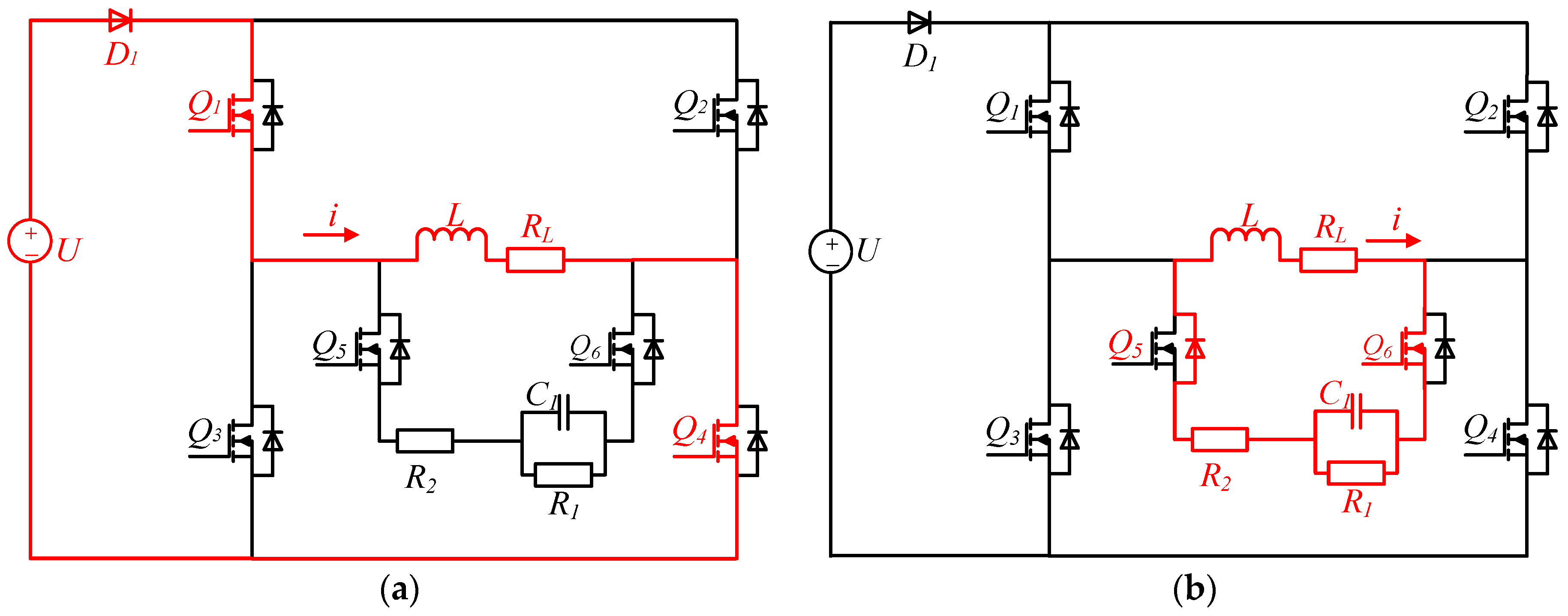
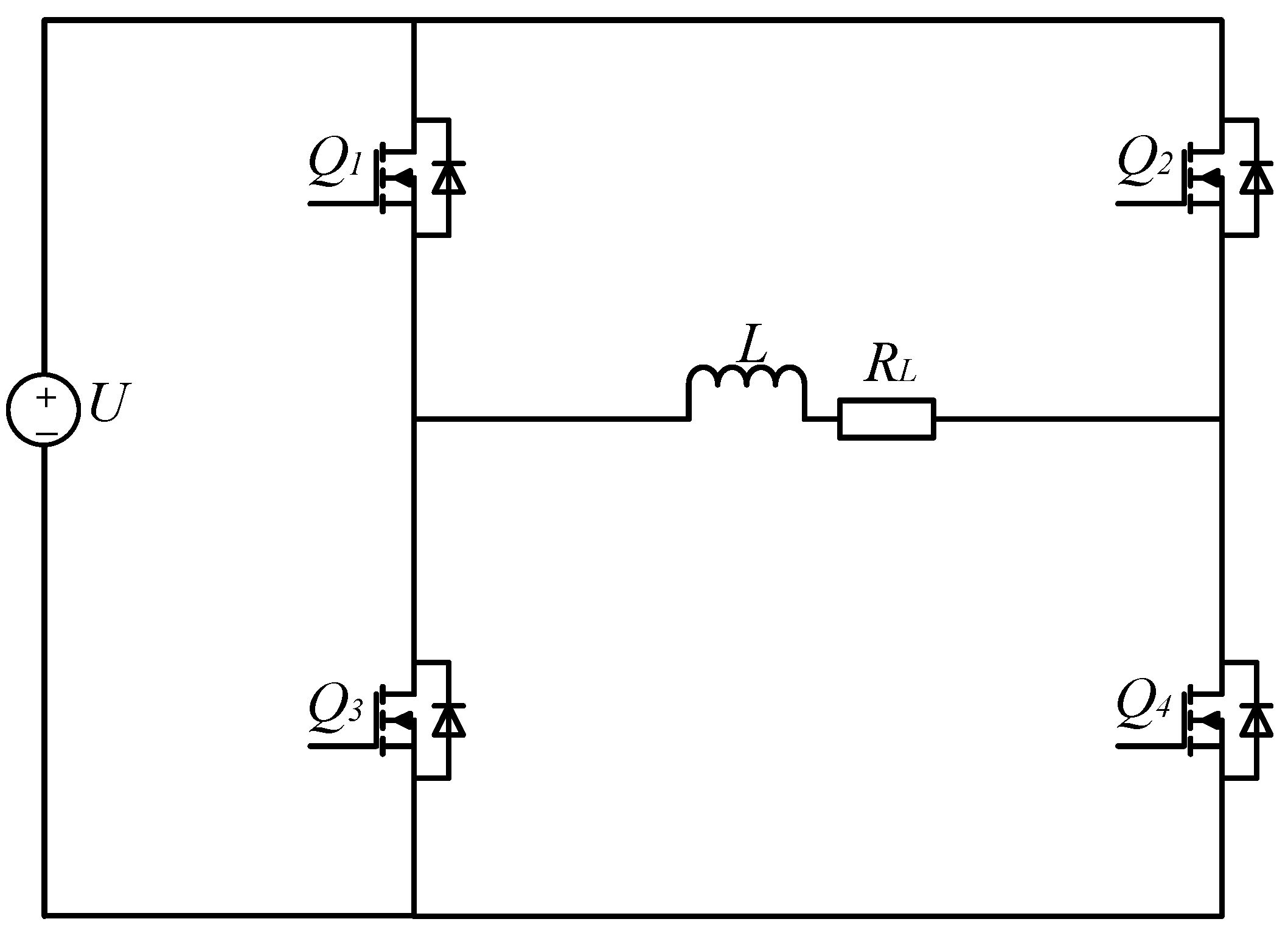
2. Proposed Topology
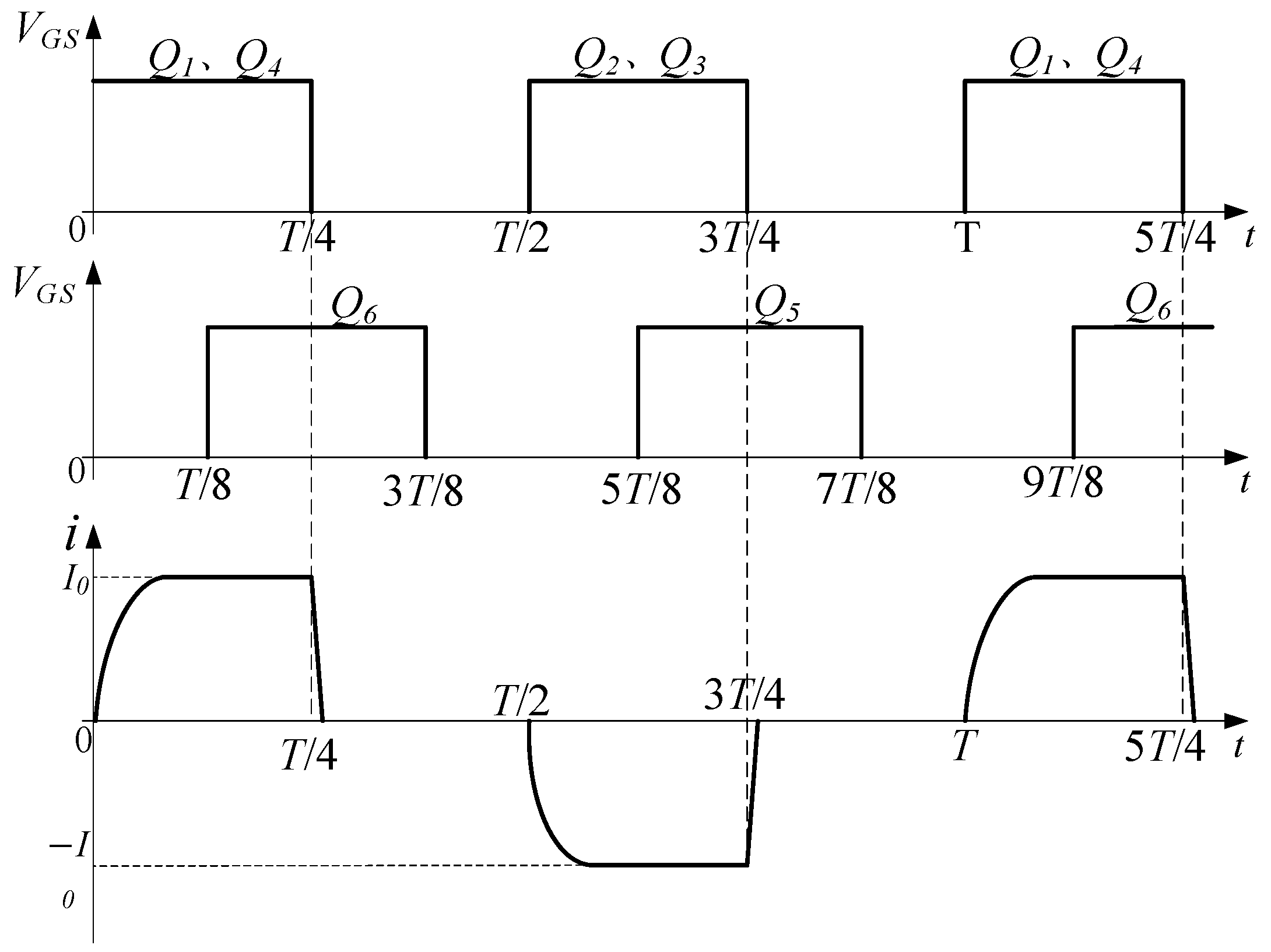
2.1. Operation Principle
- 1.
- Before the load current drops to zero, has the same function as , namely to accelerate the energy consumption of the load;
- 2.
- After the current drops to zero, there is still energy stored in . At this time, and have formed a loop, and all the energy in is released through to prepare for the next discharge stage.
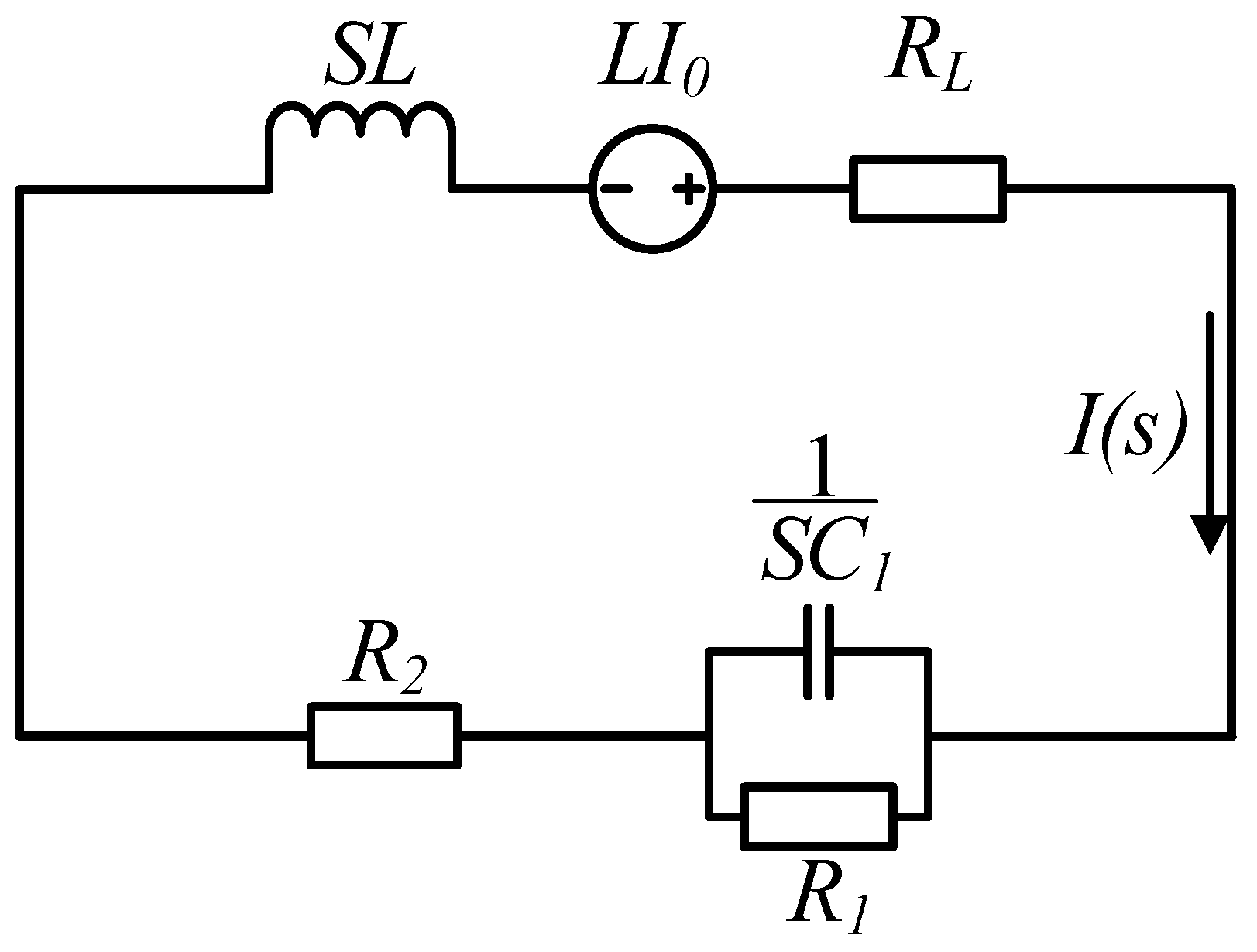
2.2. Mathematical Models Analysis
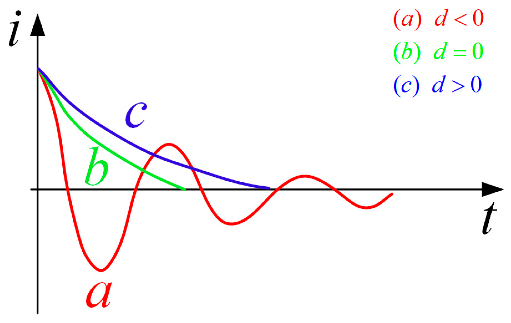
2.2.1. Mathematical Models of Turn-Off Time
- (over-damp);
- (under-damp);
- (critical-damp);
2.2.2. Mathematical Models of Voltage Stress
- ;
2.3. Numerical Analysis of the Models
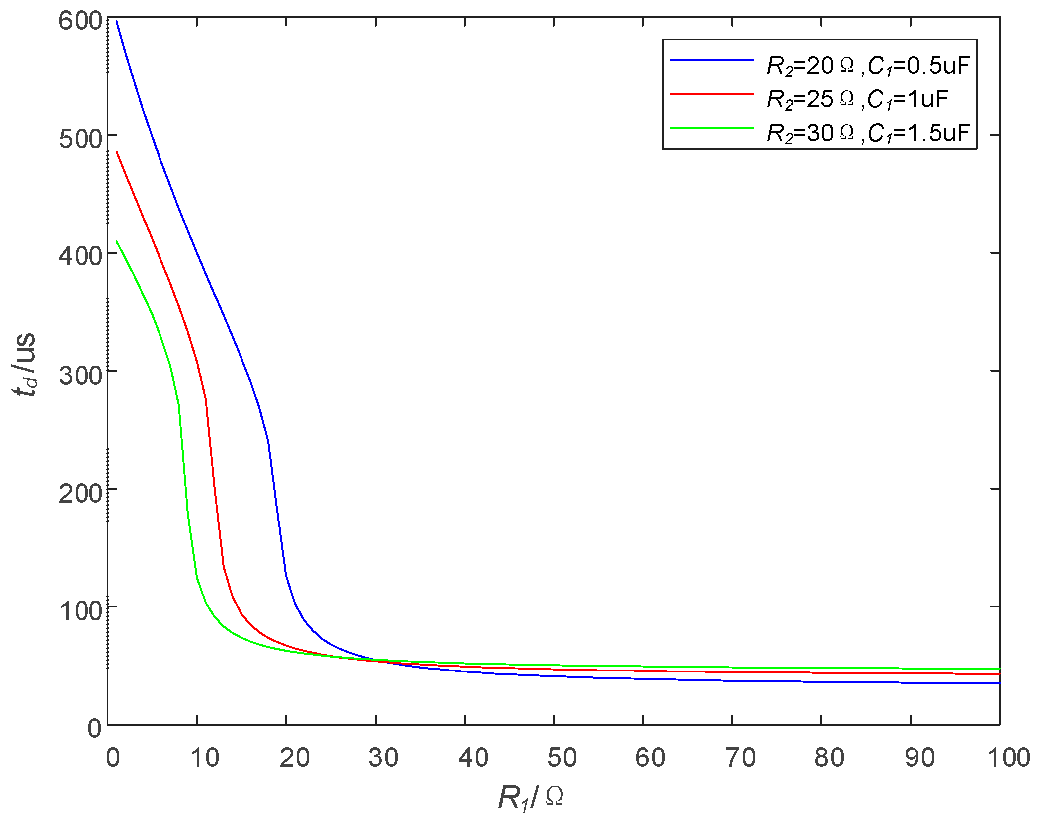
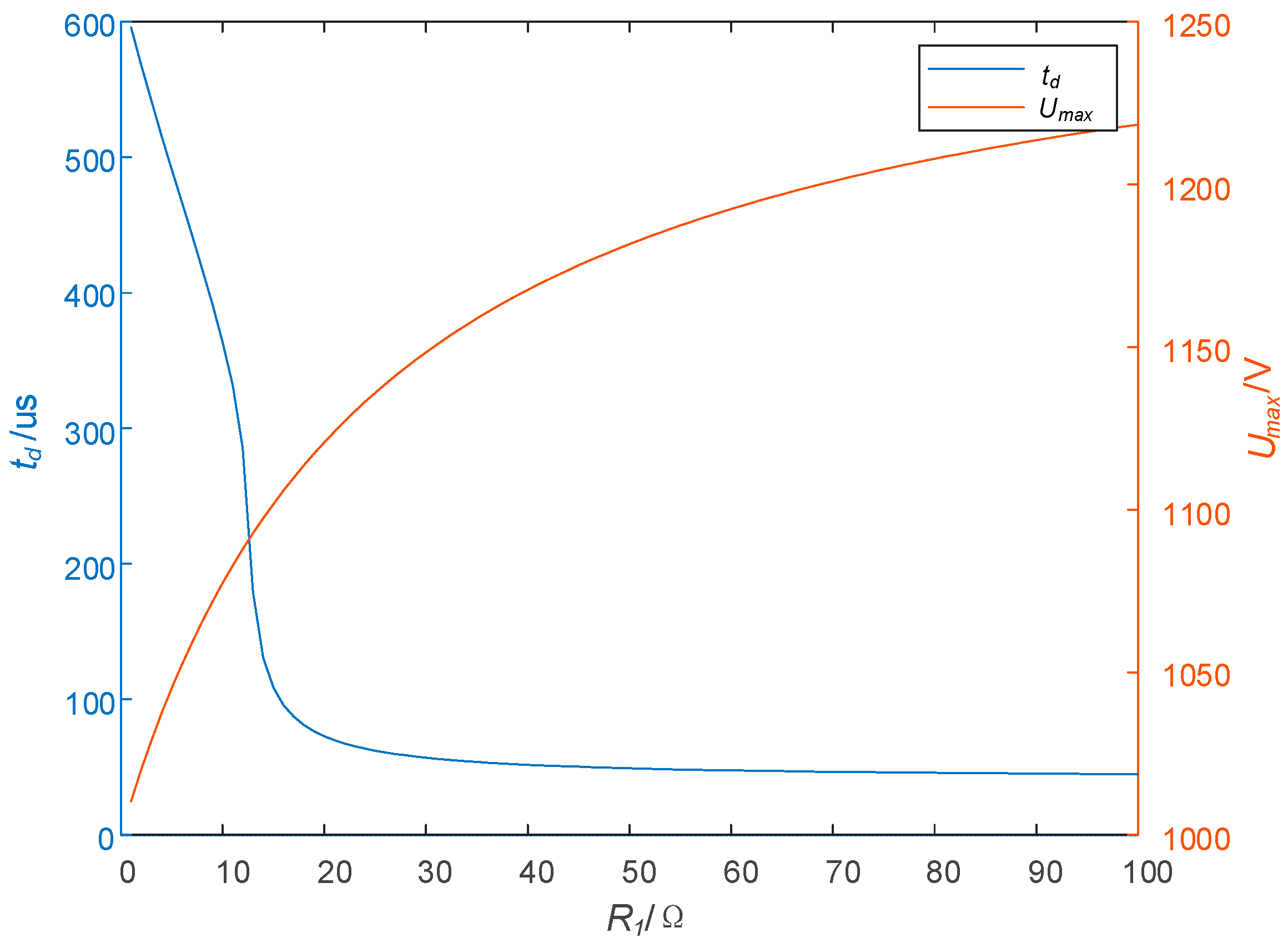
2.3.1. The Influence of on and
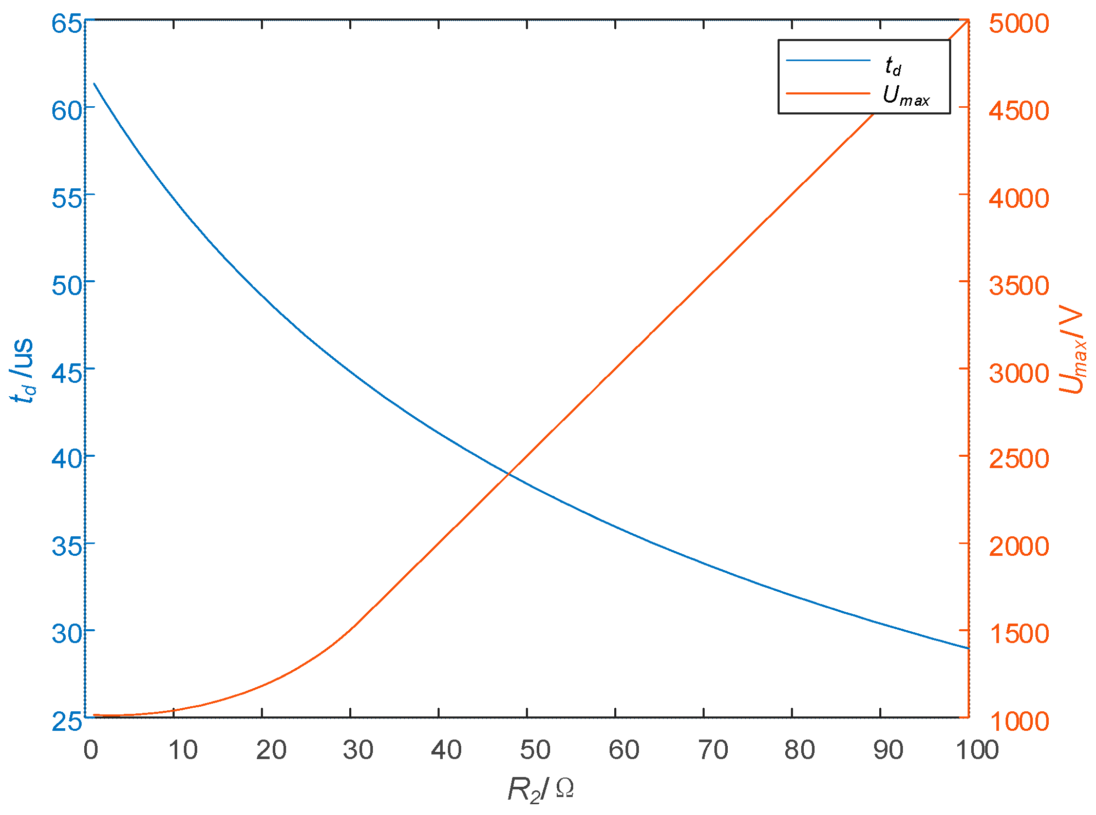
2.3.2. Effect of on and
2.3.3. Effect of on and
2.3.4. Energy Consumption Ratio Analysis
- 1.
- Second-Order Fast Turn-off Topology
- 2.
- H-bridge Topology
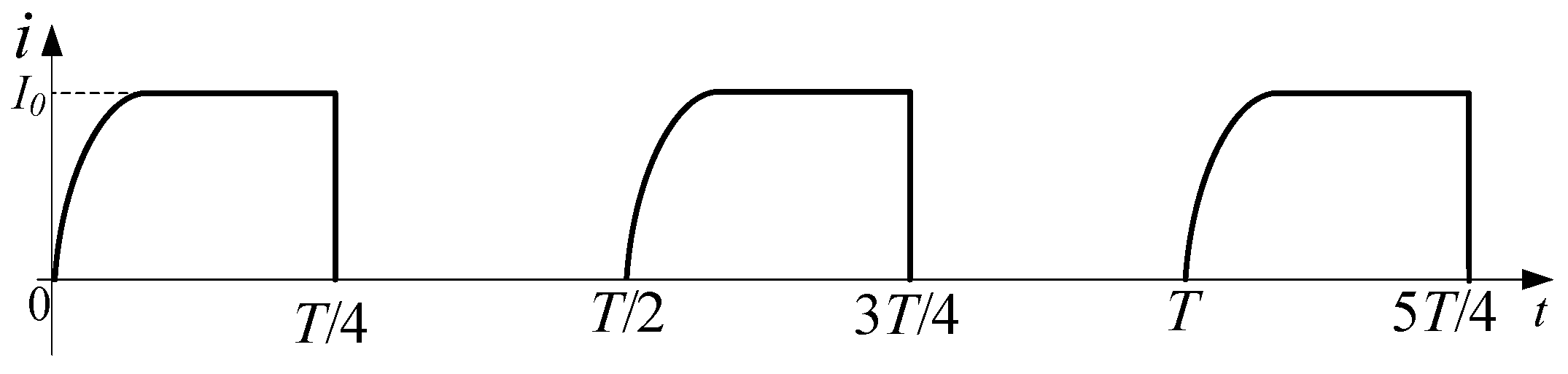
3. Simulation and Experiment
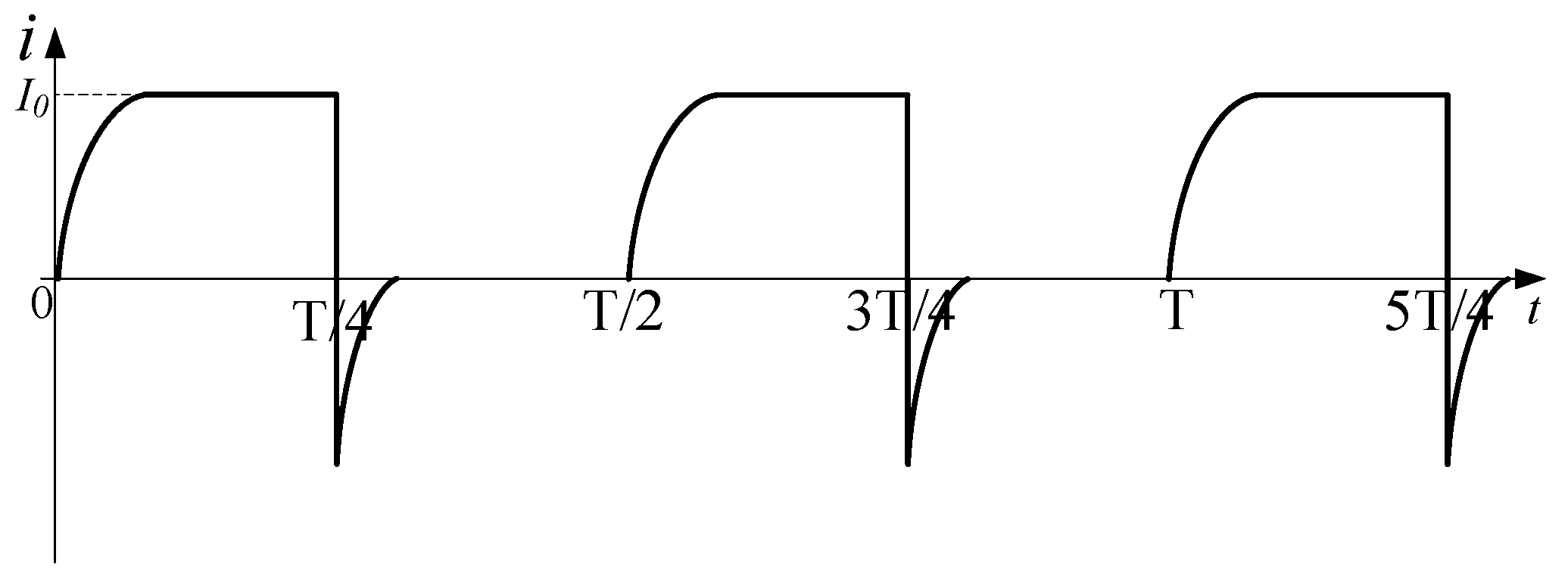
3.1. Simulation
- 1.
- Stable turn-off time: turn-off duration remains independent of current magnitude;
- 2.
- Optimized turn-off performance:
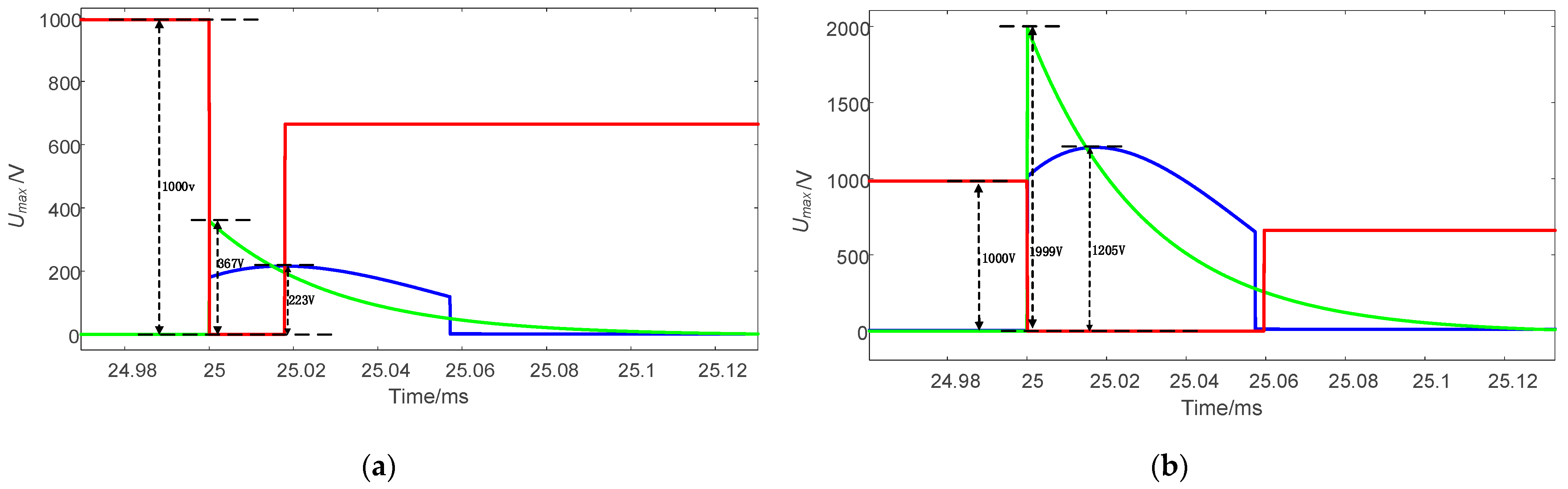
- At 50 A, the proposed topology achieves the shortest turn-off time;
- At 9 A, while reference [23] exhibits a shorter turn-off time than the proposed topology, this solution requires additional integration of a 1000 V high-voltage power supply. Such implementation not only increases system complexity but also introduces potential safety risks;
- 3.
- Voltage stress reduction: across the 9–50 A current range, the proposed topology reduces voltage stress to below 60% of reference [21]. In contrast, the high-voltage characteristics of reference [23] necessitate high-voltage-rated devices across all operating conditions. The proposed topology enables flexible selection of voltage-rated devices based on specific current magnitudes.
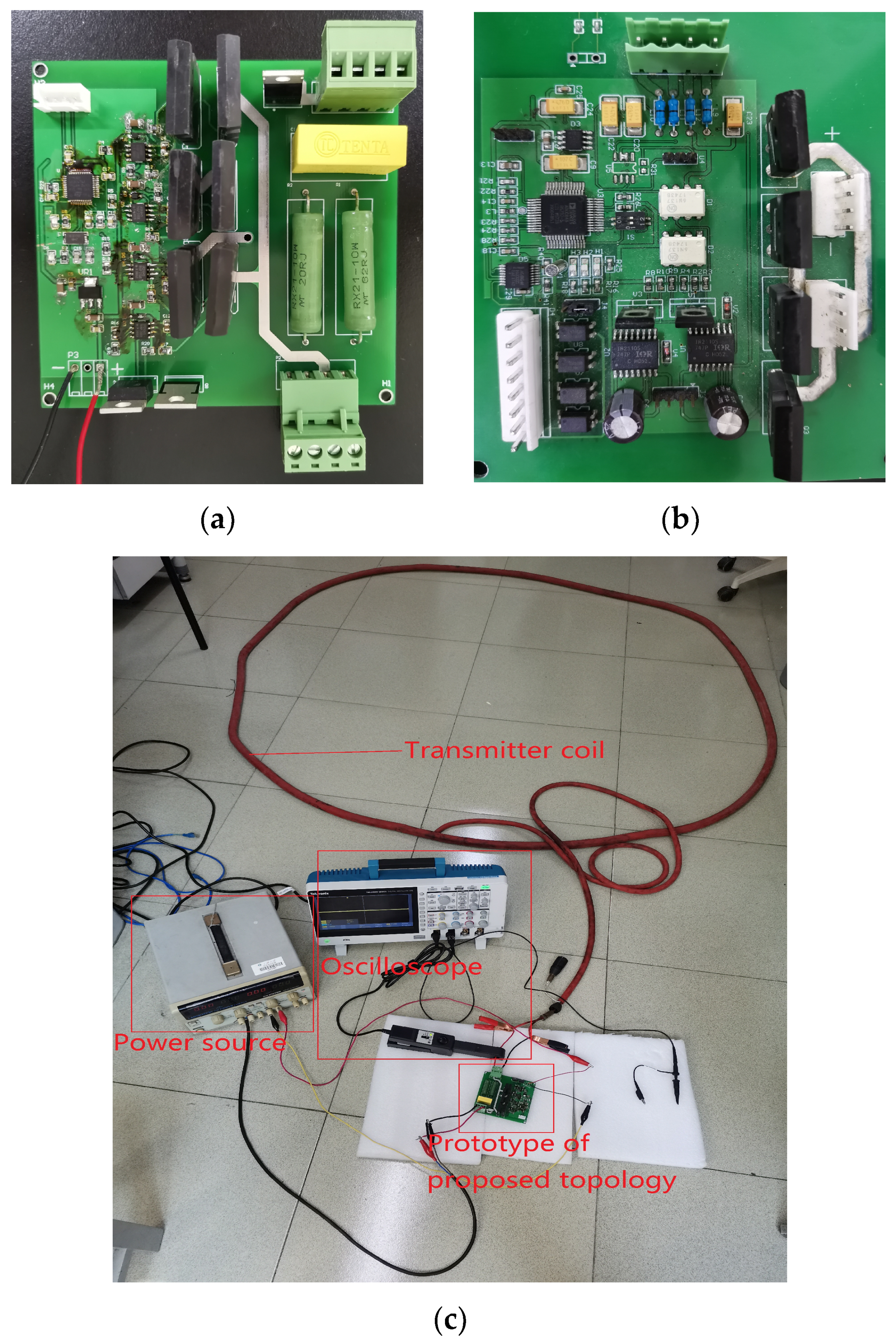
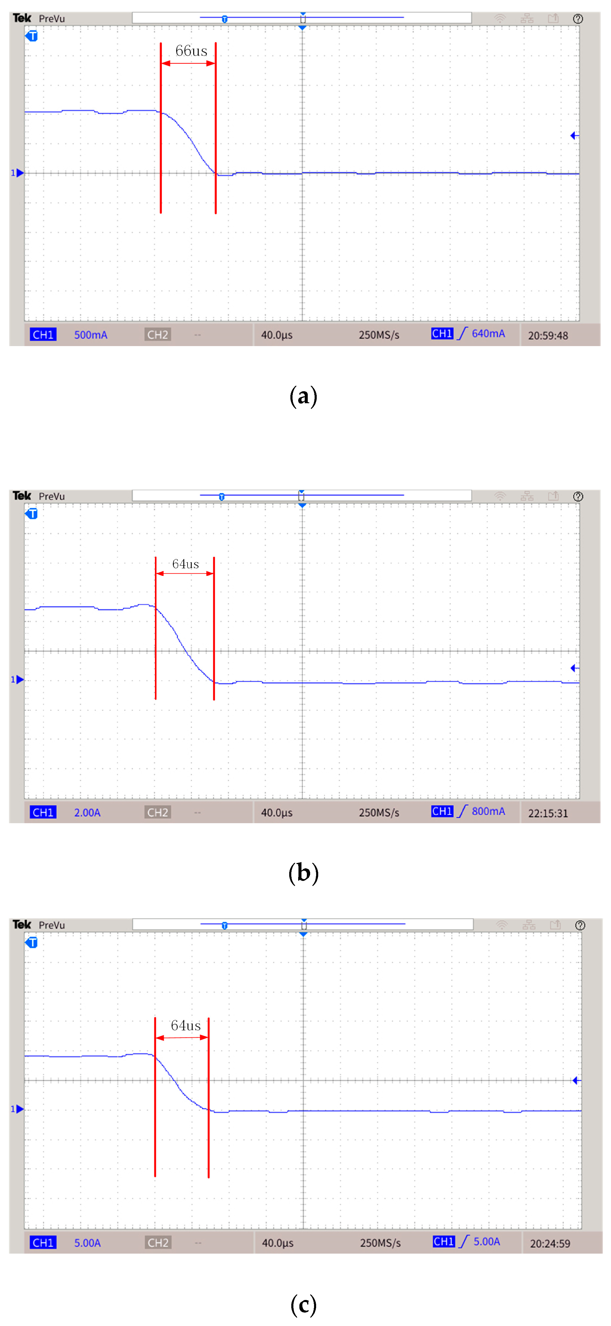
3.2. Experimental Results
4. Conclusions
Author Contributions
Funding
Institutional Review Board Statement
Informed Consent Statement
Data Availability Statement
Conflicts of Interest
References
- Peng, F.; Guo, C.; Chang, Z.; Yan, Z.; Zhao, Q.; Huang, X. A Nine-Level Inverter with Adjustable Turn-Off Time for Helicopter Transient Electromagnetic Detection. Sensors 2023, 23, 1950. [Google Scholar] [CrossRef] [PubMed]
- Su, M.; Ma, X.; Xue, Y.; Cheng, K.; Wang, P.; Liu, Y.; Yang, F. Application of the Small Fixed-Loop Transient Electromagnetic Method in Detecting Grottoes Seepage Channel. Environ. Earth Sci. 2023, 82, 45. [Google Scholar]
- Ke, Z.; Liu, L.; Jiang, L.; Yan, S.; Ji, Y.; Liu, X.; Fang, G. A New Weak-Coupling Method with Eccentric Dual Bucking Coils Applied to the PRBS Helicopter TEM System. Sensors 2022, 22, 2675. [Google Scholar] [CrossRef] [PubMed]
- Lei, D.; Ren, H.; Fu, C.; Wang, Z.; Zhen, Q. Computation of Analytical Derivatives for Airborne TEM Inversion Using a Cole–Cole Parameterization Based on the Current Waveform of the Transmitter. Sensors 2023, 23, 439. [Google Scholar]
- Di, Q.Y.; Xue, G.; Lei, D.; Wang, Z.; Zhang, Y.; Wang, S.; Zhang, Q. Geophysical Survey over Molybdenum Mines Using the Newly Developed M-TEM System. J. Appl. Geophys. 2018, 158, 65–70. [Google Scholar]
- Wang, L.; Zhang, S.; Chen, S.; Luo, C. Fast Localization and Characterization of Underground Targets with a Towed Transient Electromagnetic Array System. Sensors 2022, 22, 1648. [Google Scholar] [CrossRef]
- Nagaishi, T.; Ota, H.; Arai, E.; Hayashi, T.; Itozaki, H. High Tc SQUID System for Transient Electromagnetic Geophysical Exploration. IEEE Trans. Appl. Supercond. 2005, 15, 749–752. [Google Scholar]
- He, Z.; Suo, X.; Hu, Z.; Shi, Y.; Shi, D.; Dong, Y. Time–Frequency Electromagnetic Method for Exploring Favorable Deep Igneous Rock Targets: A Case Study from North Xinjiang. J. Environ. Eng. Geophys. 2019, 24, 215–224. [Google Scholar]
- Liu, L.; Shi, Z.; Wu, K.; Geng, Z.; Fang, G. A Bipolar Half-Sine Current Inverter for Airship-Borne Electromagnetic (AEM) Surveying. IEEE Trans. Ind. Electron. 2017, 64, 9477–9486. [Google Scholar]
- Fu, Z.; Zhou, L. Research on High Dynamic Current Steep Impulse Transmitting Circuits for Transient Electromagnetic Method Application. Proc. CSEE 2008, 28, 44–48. [Google Scholar]
- Li, F.; Tan, Q.; Wen, L.F.; Huang, D. 3-D Transient Electromagnetic Inversion Based on Explicit Finite-Difference Forward Modeling. Appl. Geophys. 2023, 20, 310–315. [Google Scholar] [CrossRef]
- Cheng, J.; Xue, J.; Zhou, J.; Dong, Y.; Wen, L. 2.5-D Inversion of Advanced Detection Transient Electromagnetic Method in Full Space. IEEE Access 2020, 8, 4972–4979. [Google Scholar] [CrossRef]
- Liu, F.; Lin, J.; Wang, Y.; Wang, S.; Xu, Q.; Cao, X.; Li, Z.; Chen, B. Reducing Motion-Induced Noise with Mechanically Resonant Coil Sensor in a Rigid Helicopter Transient Electromagnetic System. IEEE Trans. Ind. Electron. 2019, 67, 2391–2401. [Google Scholar] [CrossRef]
- Liu, L.; Qiao, L.; Liu, L.; Geng, Z.; Shi, Z.; Fang, G. Applying Stray Inductance Model to Study Turn-off Current in Multi-Turn Loop of Shallow Transient Electromagnetic Systems. IEEE Trans. Power Electron. 2020, 35, 1711–1720. [Google Scholar] [CrossRef]
- Aigner, L.; Högenauer, P.; Bücker, M.; Flores Orozco, A. A Flexible Single Loop Setup for Water-Borne Transient Electromagnetic Sounding Applications. Sensors 2021, 21, 6624. [Google Scholar] [CrossRef]
- Fu, Z.H.; Zhou, L.W.; Su, X.F.; Du, X. Two Novel Quasi-Resonant Steep Current Impulse Rectifying Circuits. Proc. Chin. Soc. Electr. Eng. 2006, 26, 70. [Google Scholar]
- Voncina, D.; Nastran, J. Current Source for Pulse Plating with High di/dt and Low Ripple in Steady State. In Proceedings of the IEEE International Symposium on Industrial Electronics (Cat. No.99TH8465), Bled, Slovenia, 12–16 July 1999; Volume 2, pp. 1234–1239. [Google Scholar]
- Leban, A.; Voncina, D. Pulse Current Source with High Dynamic. In Proceedings of the IEEE Region 8 EUROCON 2003. Computer as a Tool, Ljubljana, Slovenia, 22–24 September 2003. [Google Scholar]
- Liu, L.H.; Wu, K.; Geng, Z.; Zhao, H.T.; Fang, G.Y. Active constant voltage clamping technology for transient electromagnetic transmitter. Prog. Geophys. 2016, 31, 449–454. [Google Scholar]
- Zhu, X.; Su, X.; Tai, H.; Fu, Z.; Yu, C. Bipolar Steep Pulse Current Source for Highly Inductive Load. IEEE Trans. Power Electron. 2016, 31, 6169–6175. [Google Scholar] [CrossRef]
- Wang, G.; Min, D. Design of a Novel Fast Turn-Off Circuit of Transient Electromagnetic Transmitter. Ind. Mine Autom. 2016, 42, 77–80. [Google Scholar]
- Geng, Z.; Liu, L.; Li, J.; Liu, F.; Zhang, Q.; Liu, X.; Fang, G. A Constant-Current Transmission Converter for Semi-Airborne Transient Electromagnetic Surveying. IEEE Trans. Ind. Electron. 2019, 67, 542–550. [Google Scholar] [CrossRef]
- Liu, L.; Li, J.; Huang, L.; Liu, X.; Fang, G. Double Clamping Current Inverter With Adjustable Turn-off Time for Bucking Coil Helicopter Transient Electromagnetic Surveying. IEEE Trans. Ind. Electron. 2021, 68, 5405–5414. [Google Scholar] [CrossRef]
- Nilsson, J.W.; Riedel, S. Electric Circuits; Prentice Hall Press: Upper Saddle River, NJ, USA, 2010. [Google Scholar]
- Liu, H.; Wang, J.; Ji, Y. A Novel High-Step-Up Coupled-Inductor DC–DC Converter With Reduced Power Device Voltage Stress. IEEE J. Emerg. Sel. Top. Power Electron. 2019, 7, 1941–1948. [Google Scholar] [CrossRef]


| Number | /Ω | /μF | L/mH | /Ω | /A |
|---|---|---|---|---|---|
| 1 | 20 | 0.5 | 1.2 | 0.3 | 50 |
| 2 | 25 | 1 | 1.2 | 0.3 | 50 |
| 3 | 30 | 1.5 | 1.2 | 0.3 | 50 |
| Proposed | Reference [21] | Reference [23] | |
|---|---|---|---|
| f/Hz | 10 | 10 | 10 |
| L/mH | 1.2 | 1.2 | 1.2 |
| /Ω | 0.3 | 0.3 | 0.3 |
| /μF | 1.2 | \ | 480 |
| /μF | \ | \ | 480 |
| /Ω | 62, 20 | \ | \ |
| /Ω | \ | 40, 40 | \ |
| /Ω | \ | \ | 90 |
| /V | \ | \ | 1000 |
| Parameter | Performance | |
|---|---|---|
| theoretical calculation | = 1.16 μF | = 57.5 μs = 1198 V |
| actual choice | = 62 Ω, = 1.2 μF | = 57.3 μs = 1202 V |
| Propose | Reference [21] | Reference [23] | |
|---|---|---|---|
| Turn-off time (μs) at 9 A | 58 | 143 | 11 |
| turn-off time(μs) at 50 A | 58 | 143 | 60 |
| Voltage stress (V) at 9 A | 223 | 367 | 1000 |
| Voltage stress (V) at 50 A | 1205 | 1999 | 1000 |
| Proposed | H-Bridge | |
|---|---|---|
| f/Hz | 10 | 10 |
| L/mH | 1.2 | 1.2 |
| /Ω | 0.3 | 0.3 |
| /μF | 1.2 | \ |
| , /Ω | 62, 20 | \ |
| Device Type | Model | Parameters |
|---|---|---|
| SDUR1560CT | Average forward current: 15 A, Peak reverse voltage: 600 V | |
| , , , , , | FQL40N50 | Maximum D-S voltage, source maximum continuous current: 500 A |
| EWWR0010J20R0T9 | Resistance value: 20 Ω, rated power: 10 W | |
| EWWR0010J62R0T9 | Resistance value: 62 Ω, rated power: 10 W | |
| X2Q3125KT1B0265220125ES0 | Capacitance value: 1.2 μF, maximum continuous AC voltage: 310 V |
Disclaimer/Publisher’s Note: The statements, opinions and data contained in all publications are solely those of the individual author(s) and contributor(s) and not of MDPI and/or the editor(s). MDPI and/or the editor(s) disclaim responsibility for any injury to people or property resulting from any ideas, methods, instructions or products referred to in the content. |
© 2025 by the authors. Licensee MDPI, Basel, Switzerland. This article is an open access article distributed under the terms and conditions of the Creative Commons Attribution (CC BY) license (https://creativecommons.org/licenses/by/4.0/).
Share and Cite
Tan, C.; Yuan, S.; Yu, L.; Chen, Y.; He, C. A Second-Order Fast Discharge Circuit for Transient Electromagnetic Transmitter. Sensors 2025, 25, 2224. https://doi.org/10.3390/s25072224
Tan C, Yuan S, Yu L, Chen Y, He C. A Second-Order Fast Discharge Circuit for Transient Electromagnetic Transmitter. Sensors. 2025; 25(7):2224. https://doi.org/10.3390/s25072224
Chicago/Turabian StyleTan, Chao, Shibin Yuan, Linshan Yu, Yaohui Chen, and Changjiang He. 2025. "A Second-Order Fast Discharge Circuit for Transient Electromagnetic Transmitter" Sensors 25, no. 7: 2224. https://doi.org/10.3390/s25072224
APA StyleTan, C., Yuan, S., Yu, L., Chen, Y., & He, C. (2025). A Second-Order Fast Discharge Circuit for Transient Electromagnetic Transmitter. Sensors, 25(7), 2224. https://doi.org/10.3390/s25072224