Article

Preparation of NiO NWs by Thermal Oxidation for Highly Selective Gas-Sensing Applications

1
Sensor Laboratory, Dipartimento di Ingegneria dell’Informazione, Università degli Studi di Brescia, Via Valotti 9, 25123 Brescia, Italy
2
School of Electrical Engineering, Korea Advanced Institute of Science and Technology (KAIST), 291 Daehak-ro, Yuseong-gu, Daejeon 34141, Republic of Korea
*
Author to whom correspondence should be addressed.
Sensors 2025, 25(7), 2075; https://doi.org/10.3390/s25072075
Submission received: 27 February 2025 / Revised: 20 March 2025 / Accepted: 24 March 2025 / Published: 26 March 2025
(This article belongs to the Special Issue Nanomaterials for Chemical Sensors 2023)

Abstract

:
This paper presents a novel approach for fabricating porous NiO films decorated with nanowires, achieved through sputtering followed by thermal oxidation of a metallic layer. Notably, we successfully fabricate NiO nanowires using this simple and cost-effective method, demonstrating its potential applicability in the gas-sensing field. Furthermore, by using the film of our nanowires, we are able to easily prepare NiO sensors and deposit the required Pt electrodes directly on the film. This is a key advantage, as it simplifies the fabrication process and makes it easier to integrate the sensors into practical gas-sensing devices without the need for nanostructure transfer or intricate setups. Scanning electron microscopy (SEM) reveals the porous structure and nanowire formation, while X-ray diffraction (XRD) confirms the presence of the NiO phase. As a preliminary investigation, the gas-sensing properties of NiO films with varying thicknesses were evaluated at different operating temperatures. The results indicate that thinner layers exhibit superior performances. Gas measurements confirm the p-type nature of the NiO samples, with sensors showing high responsiveness and selectivity toward NO2 at an optimal temperature of 200 °C. However, incomplete recovery is observed due to the high binding energy of NO2 molecules. At higher temperatures, sufficient activation energy enables a full sensor recovery but with reduced response. The paper discusses the adsorption–desorption reaction mechanisms on the NiO surface, examines how moisture impacts the enhanced responsiveness of Pt-NiO (2700%) and Au-NiO (400%) sensors, and highlights the successful fabrication of NiO nanowires through a simple and cost-effective method, presenting a promising alternative to more complex approaches.

1. Introduction

High-performance gas sensors are attracting significant interest due to their wide-ranging applications in areas like chemical detection, medical and healthcare industries, and food processing and packaging. They allow for the controlling of pollution, the monitoring of gas concentrations and the ensuring of safety. Daily, the emission of air pollutants from sources like combustion engines and automobiles continues to rise. Among these, NO2 is one of the prevalent pollutants in the atmosphere, contributing to environmental issues such as acid rain, depletion of the ozone layer, and various respiratory diseases. Long-term exposure can contribute to the development of asthma and can make individuals more susceptible to respiratory infections. NO2, along with other nitrogen oxides (NOx), also contributes to the formation of harmful particulate matter and ozone, as well as acid rain, which damages ecosystems. Therefore, developing an efficient NO2 sensor is crucial for environmental monitoring and taking care of human health against excessive exposure. Traditional gas sensors for NO2 detection have utilized materials such as metal oxides (SnO2, ZnO, WO3, TiO2, Fe2O3, V2O5, CuO, NiO, etc.). Usually, metal oxides must be nanostructured to enhance the transducer function where controlling the morphology, the size, and the crystallinity can directly influence the carrier transport and, thus, the sensing response. Nanowires (NWs) are well recognized for this purpose as they limit conduction pathways along their axes and reduce the scattering phenomenon on the grain boundaries [1]. The design of single NWs provides a well-defined and reproducible path for charge carriers. This results in higher sensitivity in detecting gas molecules. A single tin oxide nanowire (60 nm in diameter, 3.5 μm long) is reported in reference [2] for a gas-sensing application, showing a good recognition of gases with a precision of 94.3% and a very low limit of detection (LOD < 1 ppm). The effect of a SnO2 nanowire’s size is studied in reference [3], which proves the depletion layer model. Compared to vertically aligned nanowires that have issues with uniformity and alignment precision over large areas, single nanowires can be individually optimized and positioned, which is still challenging and labor-intensive, often requiring advanced lithography techniques. Single NWs may also be fragile and prone to breakage, which may affect their long-term reliability and robustness in practical environments. Both architectures, while offering significant advantages in sensitivity and selectivity, face fabrication complexity, scalability, and integration challenges into electronic systems.
Random NW networks can offer a balanced approach that combines the sensitivity and functionality of nanowire-based sensors with simplified fabrication. Chemical vapor deposition (CVD), electrospinning, hydrothermal approaches, vapor–liquid–solid processes, and thermal oxidation are commonly used to prepare such NW structures [4,5,6,7,8,9,10,11]. In the following, we focus our interest on the thermal oxidation technique as it is a relatively simple and cost-effective method that provides good control of the thickness of the oxide layer by adjusting the oxidation time and temperature, allowing for fine-tuning of the nanowire properties. Moreover, it is compatible with a wide range of substrates and its process typically involves environmentally benign reactants (oxygen and water vapor). An additional reason for selecting thermal oxidation for NiO growth is the limited amount of research using this technique to prepare NiO nanowires, unlike ZnO, WO3, TiO2, and CuO materials [11,12,13,14,15,16]. N-type metal oxides are the most extensively studied semiconductors, while p-type metal oxides, which constitute only 10%, are less frequently explored [17]. We specify NiO as a promising p-type material known for its electrical properties, chemical stability, and catalytic activity, making it advantageous for applications such as gas sensing. However, it is challenging to synthesize high-quality NiO nanowires due to difficulties in controlling their morphology and crystallinity. NiO is also investigated herein because thermally oxidized NiO nanowires have not been previously reported for gas testing, which will be the challenge for this paper. Thermal oxidation of performed Ni nanowires is commonly found in the literature. Ren et al. [18] prepared NiO NWs by thermal oxidation from Ni NWs prepared by electrodeposition into anodic aluminum oxide (AAO) membranes, which are fabricated through a two-step anodization process and modified with phosphoric acid to form a through-pore template. After dissolving the template, the Ni nanowires were dispersed in ethanol and transferred onto a silicon nitride membrane for thermal oxidation. Xiang et al. also used thermal oxidation for Ni NWs synthesized via a chemical reduction-dropping method [19] by dissolving sodium hydroxide in ethylene glycol, followed by the addition of hydrazine hydrate as a reducing agent. The solution is heated to 80 °C in a magnetic field before nickel chloride hexahydrate solution is added dropwise, forming a black product [20]. A magnetic field is applied to collect the nanowires, which are then washed and dried at 60 °C for 12 h. The oxidation of Ni NWs at different temperatures shows significant changes in morphology. At 400 °C, the needle-like structures disappear, surface roughness decreases, and small cavities appear at the ends of the NWs. Increasing the temperature to 500–600 °C transforms the wire-like structures into tube-like structures, forming nanotubes (NTs) [19]. The oxidation temperature greatly affects the morphology of Ni nanowires. Additionally, previous experiments typically involve complex processes to form the nanowires, whereas thermal oxidation of a metallic nickel film is much simpler. Several studies have reported that oxidation of Ni film results in granular and porous structures [21,22,23,24,25]. In 2016, Zhu et al. [26] pioneered NiO nanowire growth via thermal oxidation of Ni foil, using an environment transmission electron microscope (ETEM) at 500 °C with controlled O2 pressure. Later studies in 2021 [27] and 2022 [28] oxidized 300 nm Ni NPs in an environment scanning electron microscope (ESEM) with oxygen/water vapor at 800 °C, achieving NiO nanorods. Koga and Hirasawa [29] used rapid oxidation up to 900 °C on laser-ablated Ni NPs to produce NiO nanorods. In contrast, our work simplifies this process by thermally oxidizing a sputtered Ni thin film at 800 °C under a steady O2 flow, without complex setups, offering a more scalable approach for NiO nanowire growth. The novelty and originality of this approach are explored in the present study for its potential application in gas sensing.

2. Materials and Methods
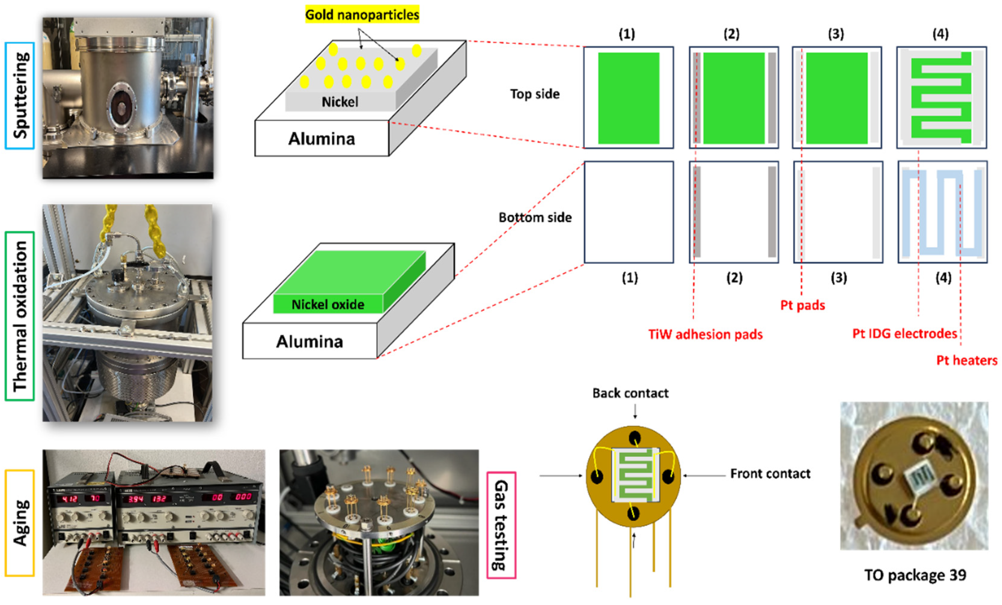
2.1. Samples

Nickel was layered through sputtering onto alumina substrates (Kyocera, Japan) with dimensions of 2 × 2 × 0.25 mm3 at room temperature for various durations. The thickness of the Ni thin film was modulated between 200 and 300 nm by adjusting the sputtering time. Subsequently, a nanolayer composed of a Au catalyst (or Pt catalyst) is applied onto the Ni layers prior to thermal oxidation to promote nanostructure growth. The oxidation process is conducted at 800 °C and 6 µbar for 4 h under an oxygen flow of 5 sccm. The samples were characterized by a Field Emission Gun Scanning Electron Microscope FEG-SEM MIRA3 from TESCAN, combined with energy dispersive X-ray spectroscopy, and a grazing incidence X-ray diffractometer which was Empyrean model, manufactured by PANalytical, Almelo, The Netherlands, working at 40 kV and 40 mA with a Cu-LFF source (λ = 1.54 Å).

2.2. Sensor Preparation

Prior to the deposition of Pt electrical contacts, the samples were heated to 300 °C and subjected to deposition of Titanium–Tungsten (TiW) as adhesion pads of 1.8 × 0.3 mm2 (step (2) of Figure 1), onto which Pt pads with were deposited (step (3) of Figure 1), followed by deposition of interdigitated electrodes on the NiO sensing layer (top side of the alumina) using a multi-fingers mask (step (4) of Figure 1) with a width of 300 µm, a length of 1 mm, and a gap space of 200 µm between adjacent fingers. Regarding the bottom side of the alumina (step (1) of Figure 1), TiW and Pt pads (steps (2) and (3) of Figure 1) were also deposited, onto which Pt electrodes were patterned as heaters (step (4) of Figure 1). After the preparation of the electrical contacts, the samples were subjected to bonding with gold wires on a transistor outline (TO 39) package and to aging at 450 °C for two days to ensure the devices’ stabilization.

2.3. Gas-Testing Conditions

The experiment involved exposing the gas sensor to different gases using 200 sccm of total flow after thermal stabilization for 10 h and testing it across different operating temperatures under humid air (relative humidity: RH = 50% @ 20 °C). Based on the sensor’s selectivity, the device was exposed to suitable gas by varying concentrations of NO2, ranging from 0.5 ppm to 5 ppm at the optimum temperature, and studying its performance in a dry environment (RH = 0% @ 20 °C). The NO2 measurements were repeated to investigate the NiO sensors’ reliability and their long-term stability. The sensors were also subjected to exposure to different gases for selectivity tests. This was carried out by sequentially injecting each gas with a 30 min dose time and a 1.5 h recovery time in a testing chamber with a volume of 1 L.
Figure 1 summarizes the experimental procedures used for growing NiO film as a gas-sensing device.

3. Results and Discussion

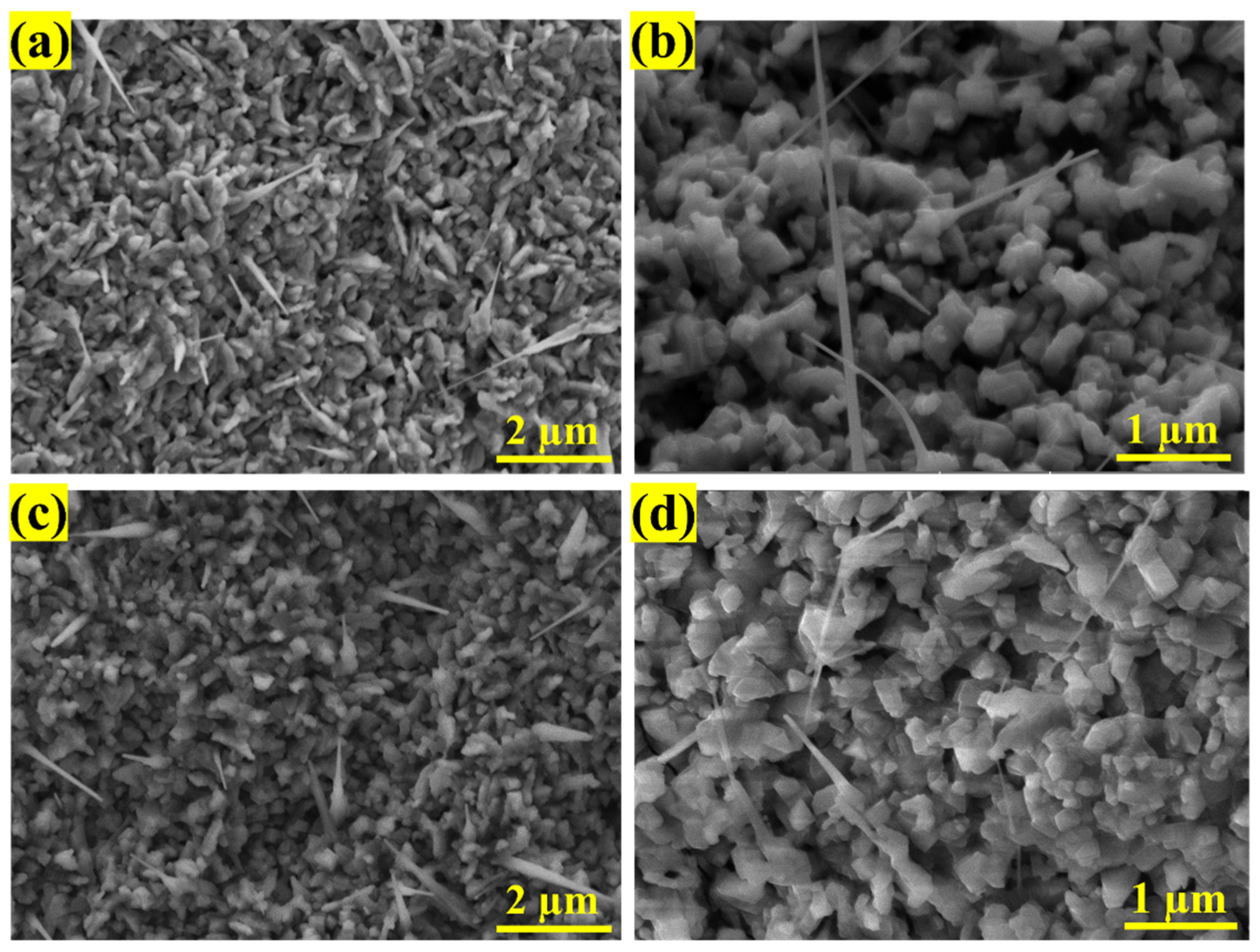
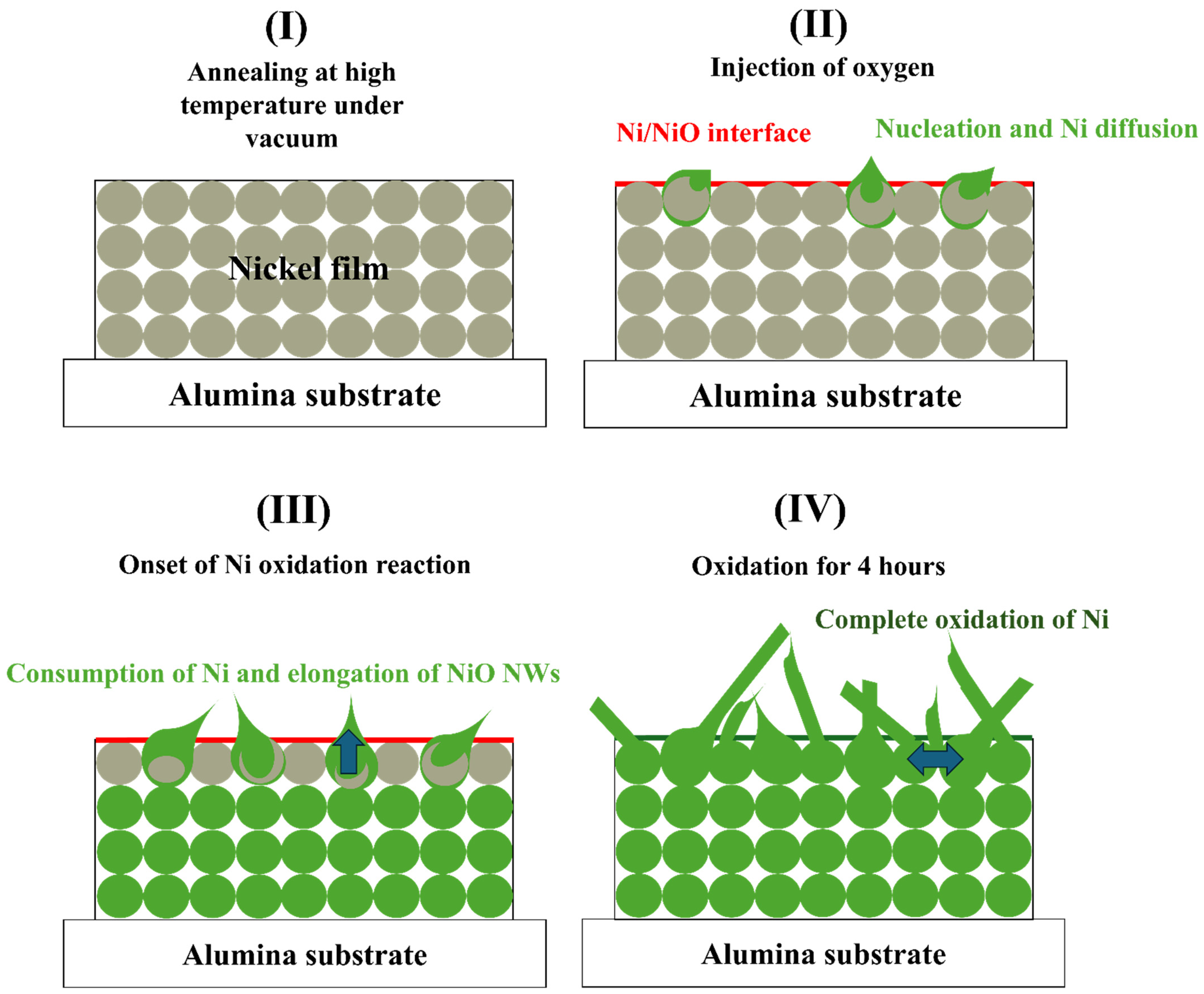
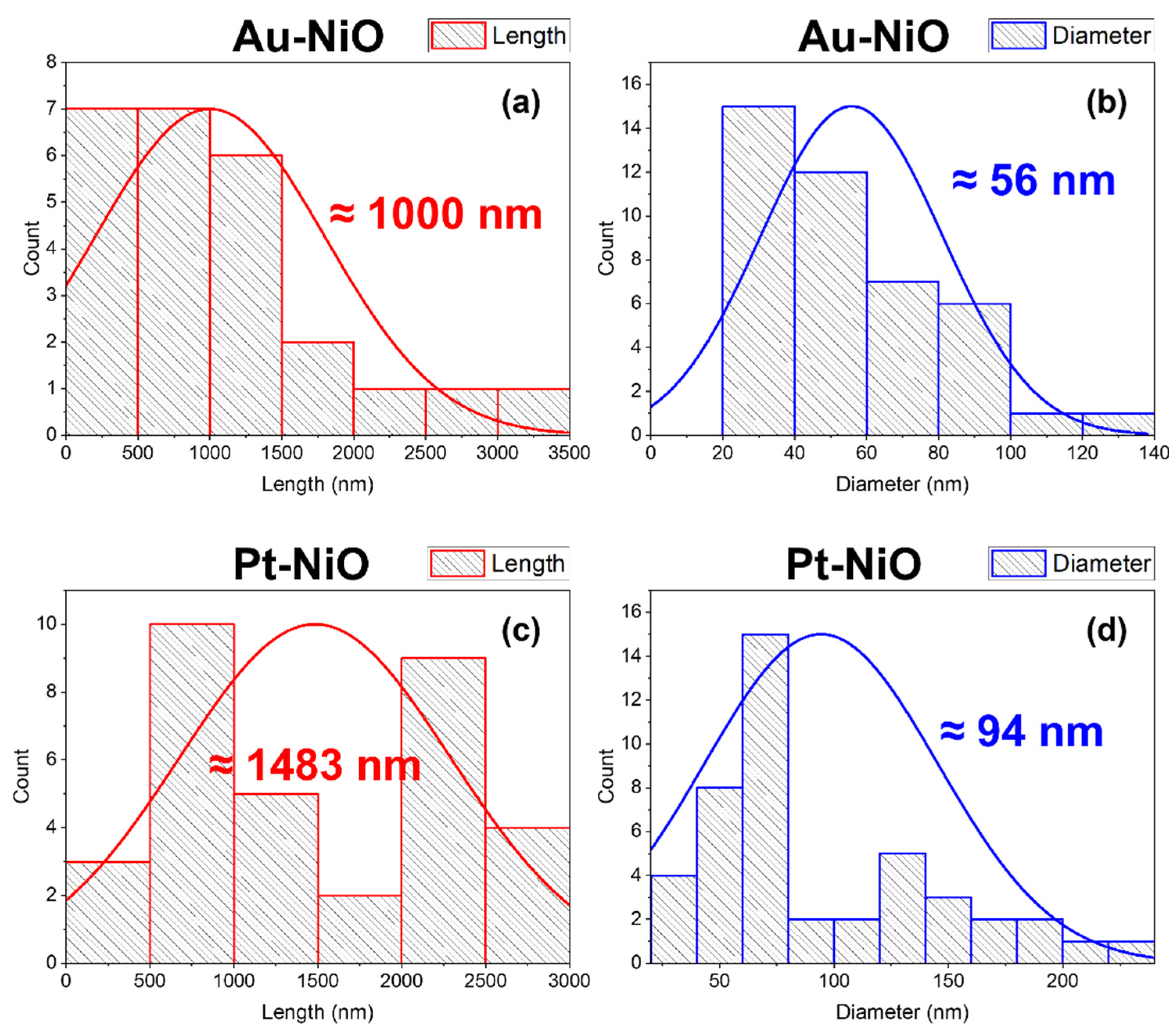
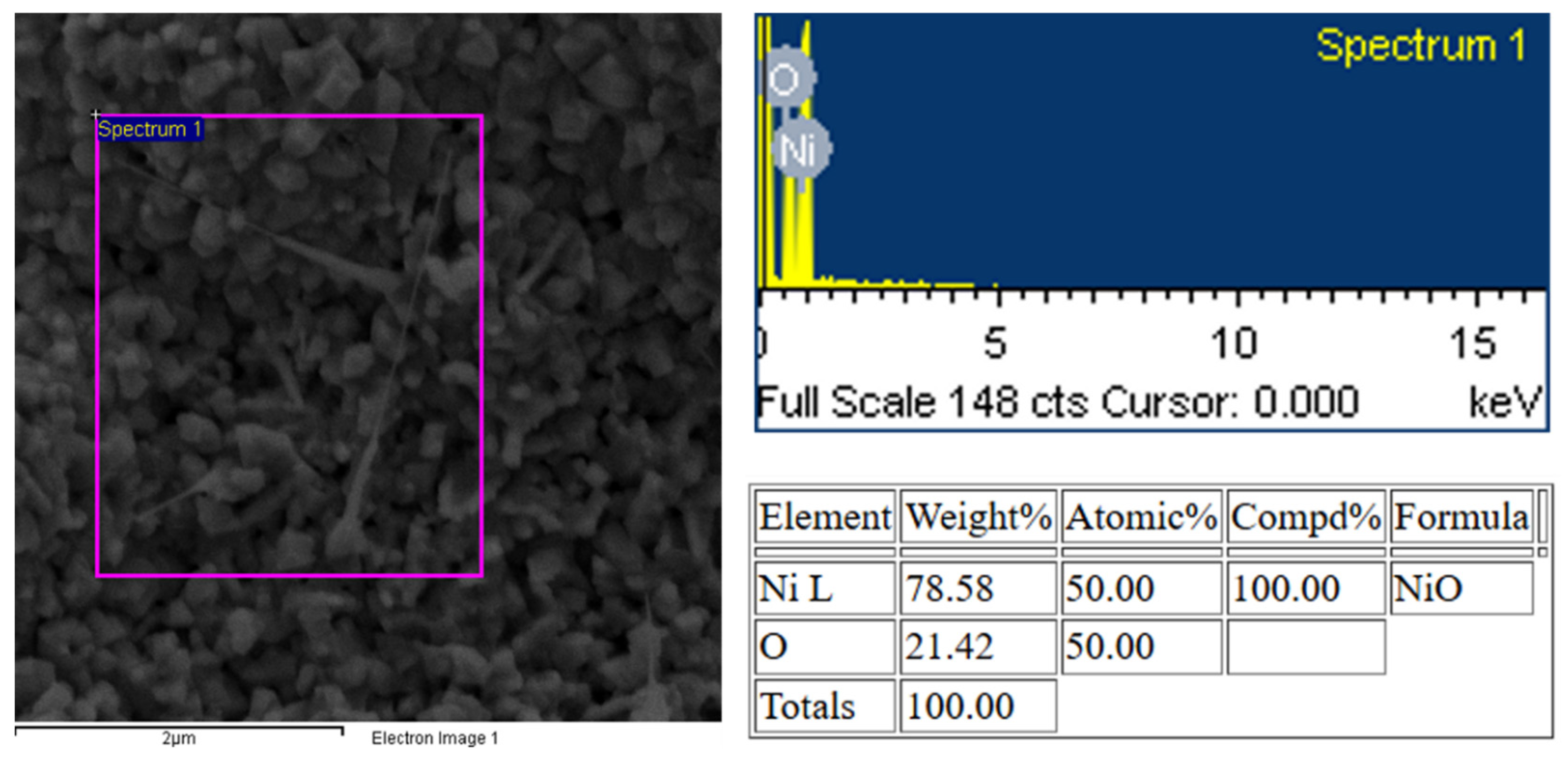
3.1. Morphology and Structural Properties

Figure 2 shows the morphologies of NiO using two catalysts, Au and Pt. One can see the co-presence of granular and porous film with distribution of randomly oriented nanowires, which allows high accessibility and adsorption of gas species. The process begins with the deposition of a nickel (Ni) layer onto an alumina substrate, followed by the addition of catalyst nanoparticles such as gold (Au) or platinum (Pt) onto the nickel surface.
To explain the observed morphology of the NiO nanowires shown in Figure 2, we propose the following growth mechanism. The catalyst particles serve as active sites that initiate the oxidation of the nickel layer upon heating, promoting the formation of oxide nuclei, which act as seeds for the growth of nickel oxide nanowires. The growth of these nanowires is further driven by stress-induced grain boundary diffusion, where nickel ions migrate through the grain boundaries to react with oxygen atoms, facilitated by an oxygen concentration gradient [30].
The formation of NiO nanowires from thermally oxidized Ni layers can be explained through a mechanism involving layer-by-layer oxidation at the Ni/NiO interface, similar to the process outlined in [28], where the authors used 300 nm of Ni NPs to be oxidized at 800 °C in an environment scanning electron microscope with oxygen/water vapor, resulting in NiO nanorods. In this mechanism, oxygen vacancies migrate along the interface plane, allowing Ni atoms to react with oxygen at kink sites, thereby driving growth along specific crystallographic directions. This process follows the Terrace Ledge Kink (TLK) model, where new NiO layers form progressively due to the migration of disconnections at the interface. As the Ni layer undergoes oxidation, Ni vacancies accumulate, leading to the gradual conversion of the Ni layer into NiO nanowires. The growth is primarily influenced by thermodynamic factors such as oxygen partial pressure and temperature, which promote oxygen migration and encourage the anisotropic formation of NiO. Over time, the Ni layer thins while NiO nanowires elongate, with growth rates governed by the balance between oxygen diffusion and interface step movement. This mechanism aligns with established crystal growth models, such as the Kossel–Stranski model, where atoms preferentially attach to energetically favorable sites, adapting to the unique conditions of Ni thermal oxidation. A detailed schematic representation of the Ni film oxidation process is provided in Figure 3.
As noted in reference [31], the optimization of small grains and large pores is essential for enhancing both the transduction process and the efficiency of gas diffusion within the entire volume of the sensing material. However, in conventional thick films, a common challenge arises where small particles tend to be associated with small pores, possibly leading to counterproductive outcomes. To address this challenge, reducing the film thickness and integrating nanowires into these granular and porous structures can be effective by improving gas adsorption on the sensing material and increasing the specific surface area [32]. This approach forms a NiO network that interconnects Pt interdigitated electrodes, facilitating efficient interaction with gas species whose sensing capabilities will be investigated in Section 3.2.
To further characterize the morphology of the NiO nanowires, we analyzed their size distribution based on SEM images. The statistical analysis revealed that the average nanowire length is approximately 1000 nm for Au-NiO and 1483 nm for Pt-NiO, while the average diameter is 56 nm for Au-NiO and 94 nm for Pt-NiO. These differences indicate that the choice of catalyst significantly influences the growth of NiO nanowires. The Pt-catalyzed nanowires exhibit a greater length and diameter compared to their Au-catalyzed counterparts, suggesting a more efficient catalytic effect in promoting nanowire elongation. This variation in morphology can be attributed to the distinct catalytic activity of Au and Pt, which affects the nucleation and diffusion kinetics of Ni species during the thermal oxidation process. The size distribution histograms of NiO nanowires for both catalysts are presented in Figure 4, providing a comprehensive view of the structural differences.
Figure 5 presents the grazing incident X-ray diffraction (GIXRD) patterns of a NiO sample oxidized at 800 °C.
The NiO phase is identified according to ICDD card 00-004-0835. The most significant Bragg’s reflection peaks correspond to crystal planes (111), (200), (220), (311), and (222) and are, respectively, located at 2 θ values of 37.32°, 43.38°, 62.92°, 75.47°, and 79.52°, with preferred orientation along (200). The other peaks are related to the alumina substrate according to ICDD cards No. 01-073-1512 and 00-001-1305. The prepared NiO structure is polycrystalline and is depicted to be a cubic single phase of bunsenite NiO with space group Fm3m: 225.
The crystallinity degree of nickel oxide (NiO) was determined based on the analysis of the X-ray diffraction (XRD) patterns presented in Figure 5. This parameter quantifies the proportion of the crystalline phase within the material, providing insights into its structural characteristics and potential impact on its electronic and gas-sensing properties. The crystallinity index was calculated by integrating the area of the crystalline peaks relative to the total area of the diffraction pattern, which includes both crystalline and amorphous contributions. The obtained value of 31.22% suggests a significant degree of structural disorder in the NiO film. This partial amorphous nature may be attributed, in part, to the influence of the alumina substrate, which can contribute to an overall reduction in crystallinity due to lattice mismatch, limited grain growth, or induced defects.
In addition to crystallinity, the XRD data also allow for the estimation of strain and stress effects within the NiO film. The broadening of diffraction peaks can be associated with microstructural strain, which arises from factors such as defects, dislocations, and lattice distortions.
The crystallite size D, dislocation density δ, and lattice strain ε for NiO were determined using the following equations [33]:
D cristallite = M   λ β   cos θ
where M = 0.9 is the dimensionless shape factor, λ = 1.54 Å is the wavelength of the incident X-ray, β is the full width at half maximum (FWHM) extracted from the XRD pattern, and θ is the Bragg diffraction angle identified from the XRD spectrum.
The dislocation density δ and lattice strain ε are calculated as:
δ = 1 D 2
β   cos θ 4
Additionally, the interplanar spacing d is determined using Bragg’s law:
d = n   λ 2   sin θ
where n represents the reflection order.
All the parameters have been estimated and are presented in Table 1.
The analysis of the NiO structure reveals that the (200) crystal plane emerges as the dominant orientation. This preferred orientation suggests that the synthesis conditions favored the growth of NiO along this specific crystallographic plane. The prominence of the (200) plane further implies that the NiO structure was formed with a stoichiometric composition, meaning the ratio of nickel to oxygen atoms aligns with the ideal 1:1 NiO formulation [34]. The EDX analysis shown in Figure 6 proves that the primary material in the sample is NiO, with a stoichiometric Ni atomic ratio of 1:1, as expected for pure nickel oxide.
Achieving such a stoichiometric balance is important, as it confirms that the structures have a well-defined and stable composition, free from significant defects like oxygen vacancies or excess nickel atoms. The formation of NiO with a dominant (200) orientation also suggests that the nanostructures may exhibit consistent surface properties, which can influence their stability, reactivity, and overall performance in applications.

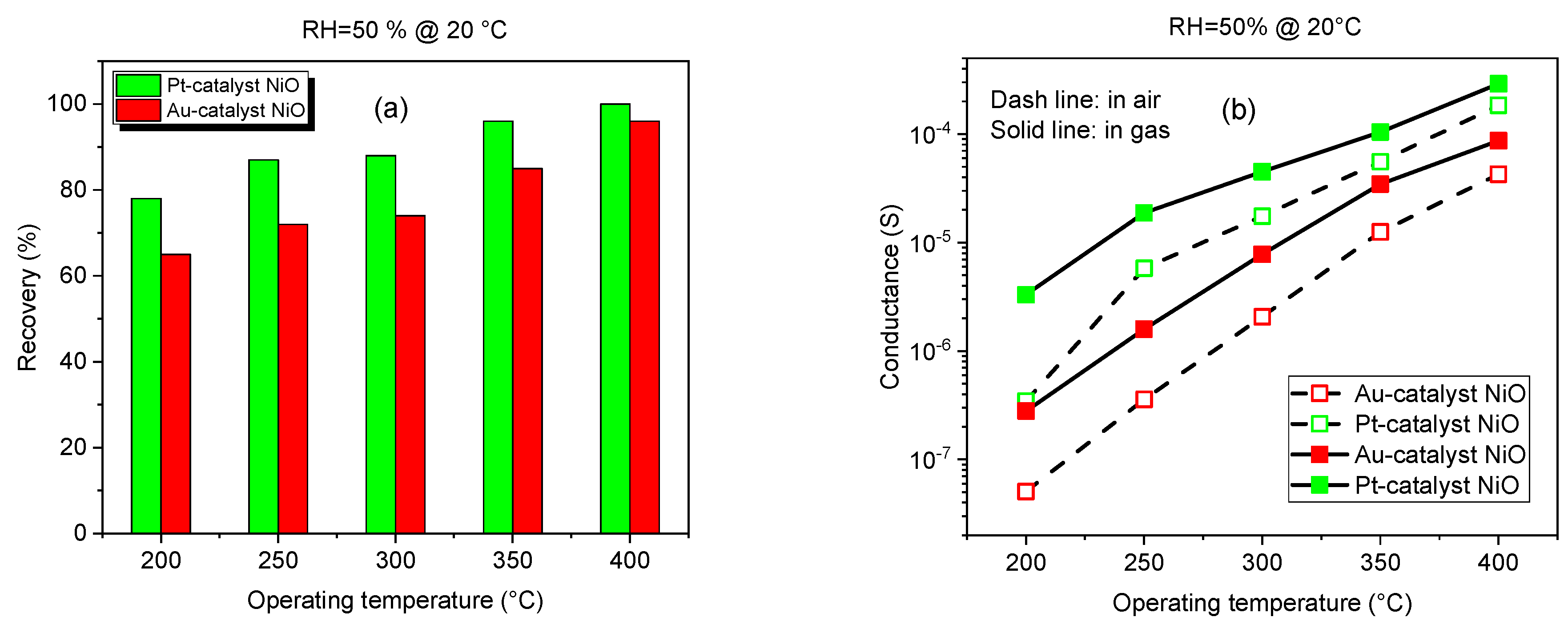
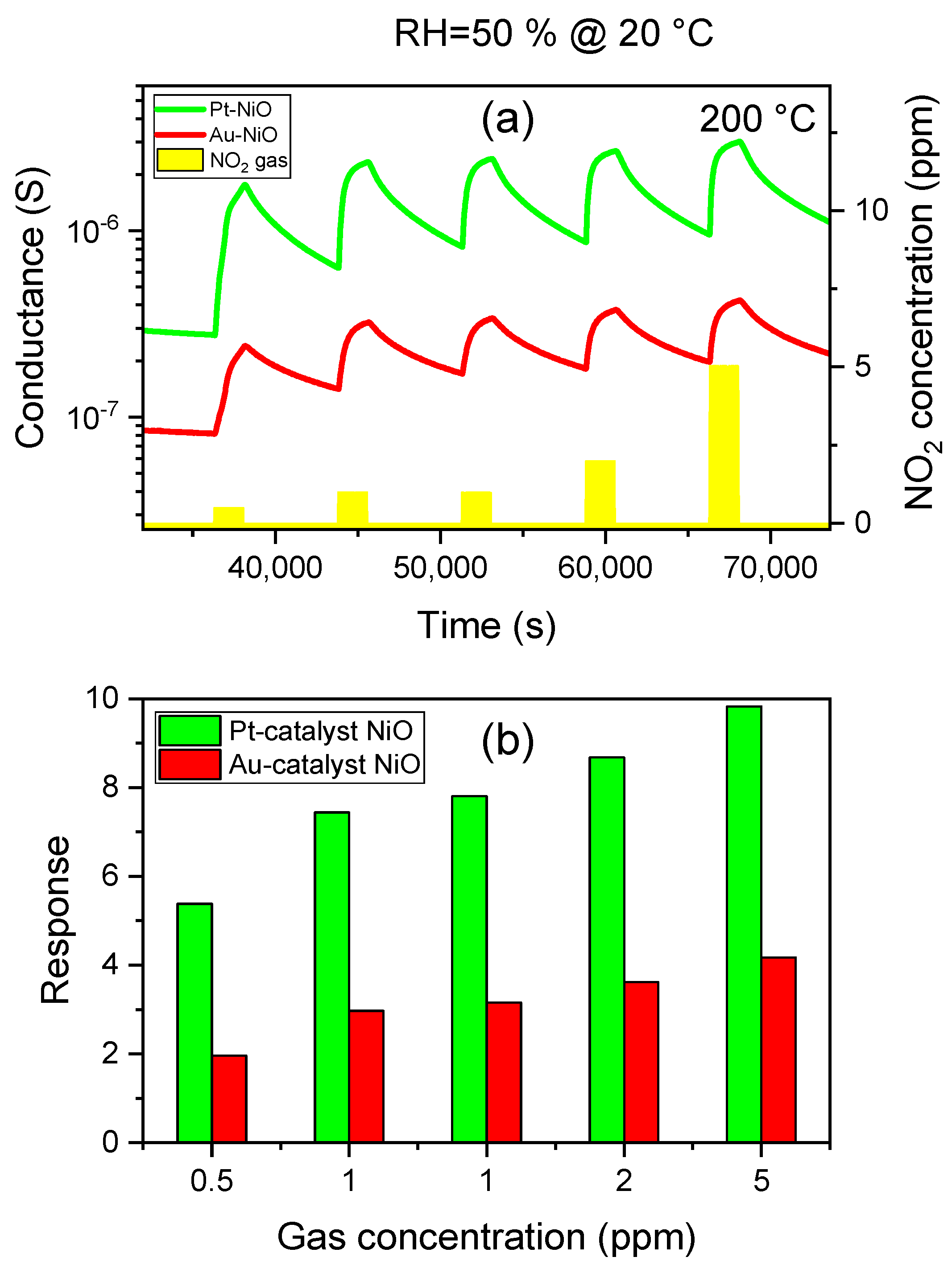
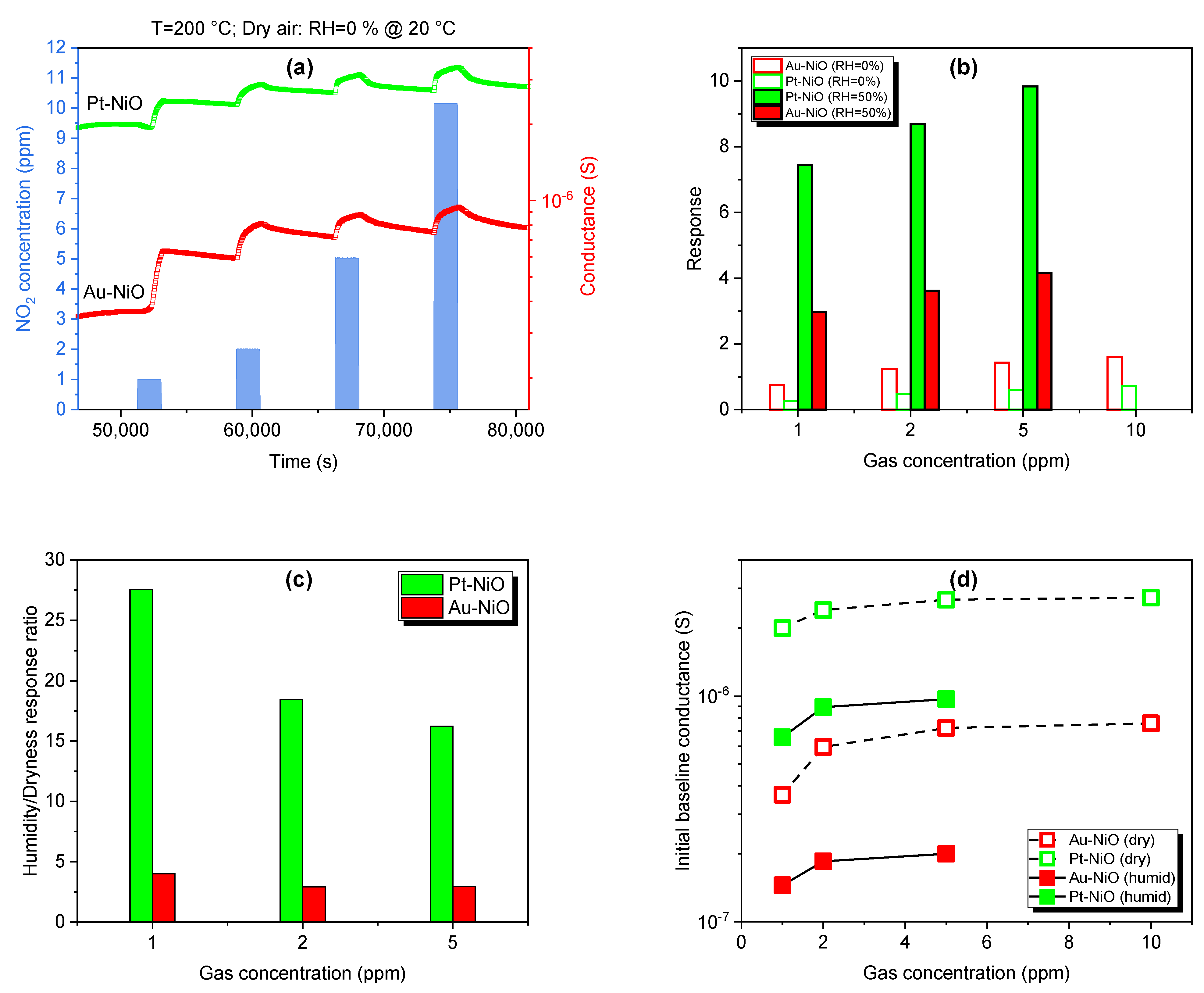
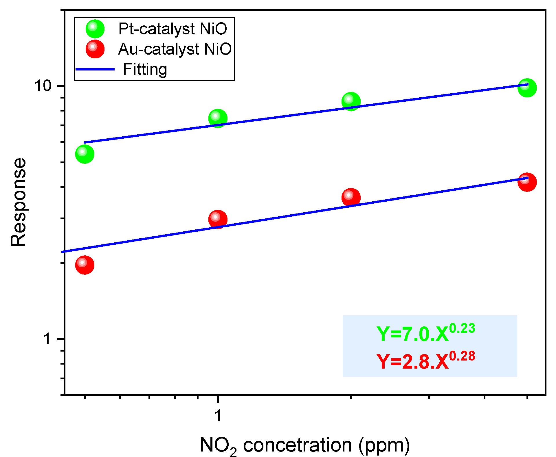
3.2. Gas-Sensing Performance

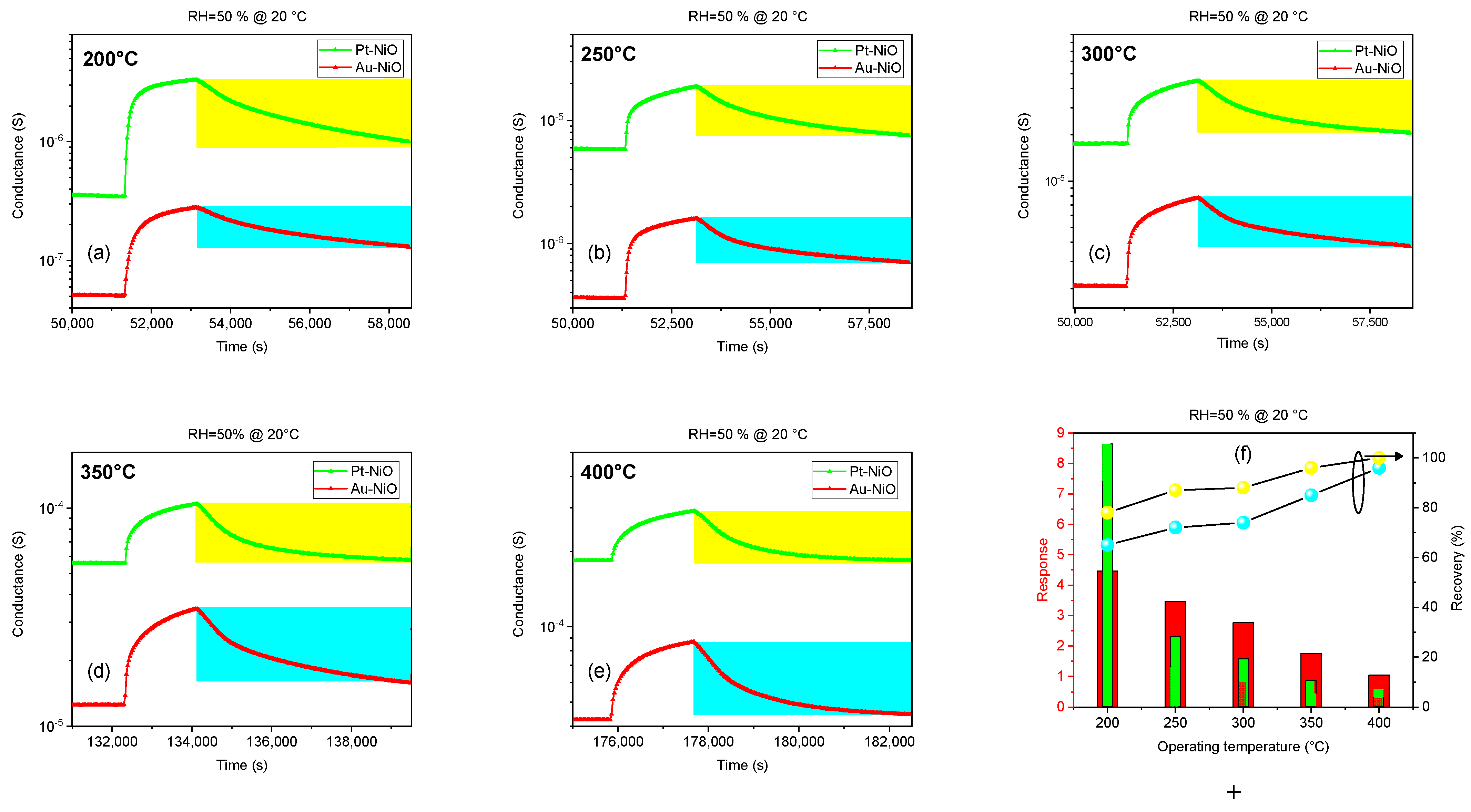
3.2.1. Gas Response at Different Operating Temperatures

Figure 7 shows the NiO response toward NO2 at different thicknesses using Au and Pt catalysts in a temperature range of 200–400 °C and in a wet air environment (relative humidity RH = 50%).
The optimal operating temperature of 200 °C for NiO sensors toward NO2 with varying thicknesses and catalysts is likely due to a combination of optimal surface reaction kinetics, enhanced catalyst activity, and favorable charge carrier mobility. Penza et al. reported that the gas sensitivity of multi-walled carbon nanotube (MWCNT)-based chemoresistors can be tailored by the type of surface catalyst. Specifically, platinum and gold catalysts enhance the sensitivity to NO2, respectively, due to metal-induced gap states [35]. In our NiO gas testing, platinum shows a better sensing response compared to gold that can be assigned to higher catalytic activity and more active sites for gas adsorption and reaction with NiO surfaces and NO2. Pt may modify the electronic properties of NiO more significantly than Au, enhancing the overall sensitivity of the sensor [36,37,38].
At 200 °C, the morphology of the NiO layer might be such that it provides optimal surface area and porosity for gas diffusion and interaction, leading to improved sensitivity. Also, the energy provided at 200 °C to the sensor surface is sufficient to activate the catalytic reaction between NO2 and the surface of NiO. This temperature likely offers the best balance between adsorption and desorption rates of NO2 on the NiO surface, leading to maximum response. Catalysts are often used to lower the activation energy of a chemical reaction. At 200 °C, the catalysts on the NiO surface reach an optimal activation state, facilitating efficient interaction with NO2 molecules. This can enhance the sensor’s response to NO2 by increasing the reaction rate on the surface, noting that the Pt catalyst shows a higher response compared to the Au catalyst. Thinner films (200 nm) exhibit a more pronounced response compared to thicker layers. Another explanation was reported in the literature [39] in a study of the gas concentration profile as a function of sensing layer thickness based on Knudsen diffusion and Langmuir adsorption models. It was proved that by increasing the thickness of the film, the amount of gas species adsorbed on the sensing layer decreases drastically. This behavior weakens the surface interactions with gas molecules and thus decreases the metal oxide sensor’s responsiveness. Experimental works have also found similar results for NiO sensors [40]. Temperature significantly influences the operation of gas sensors based on metal oxides. The response of NiO gas sensors is highly dependent on temperature variations, as shown in Figure 7. This dependency arises due to several factors [41]. Firstly, the adsorption and desorption rates of gas molecules onto the surface of the metal oxide are temperature dependent. At higher temperatures, the adsorption of gas molecules onto the surface of the MOX material increases, leading to a more pronounced response to the target gas. Secondly, the activation energy required for the chemical reaction between the gas molecules and the metal oxide surface also varies with temperature. At the optimal temperature (200 °C for our sensors), the activation energy is reached, resulting in efficient gas detection. Moreover, the temperature affects the conductivity of the NiO material, influencing the electrical signal generated by the sensor in response to NO2 exposure.
In the following, we will focus on Au-NiO and Pt-NiO sensors with a thickness of 200 nm, as they exhibit the highest response compared to other samples.

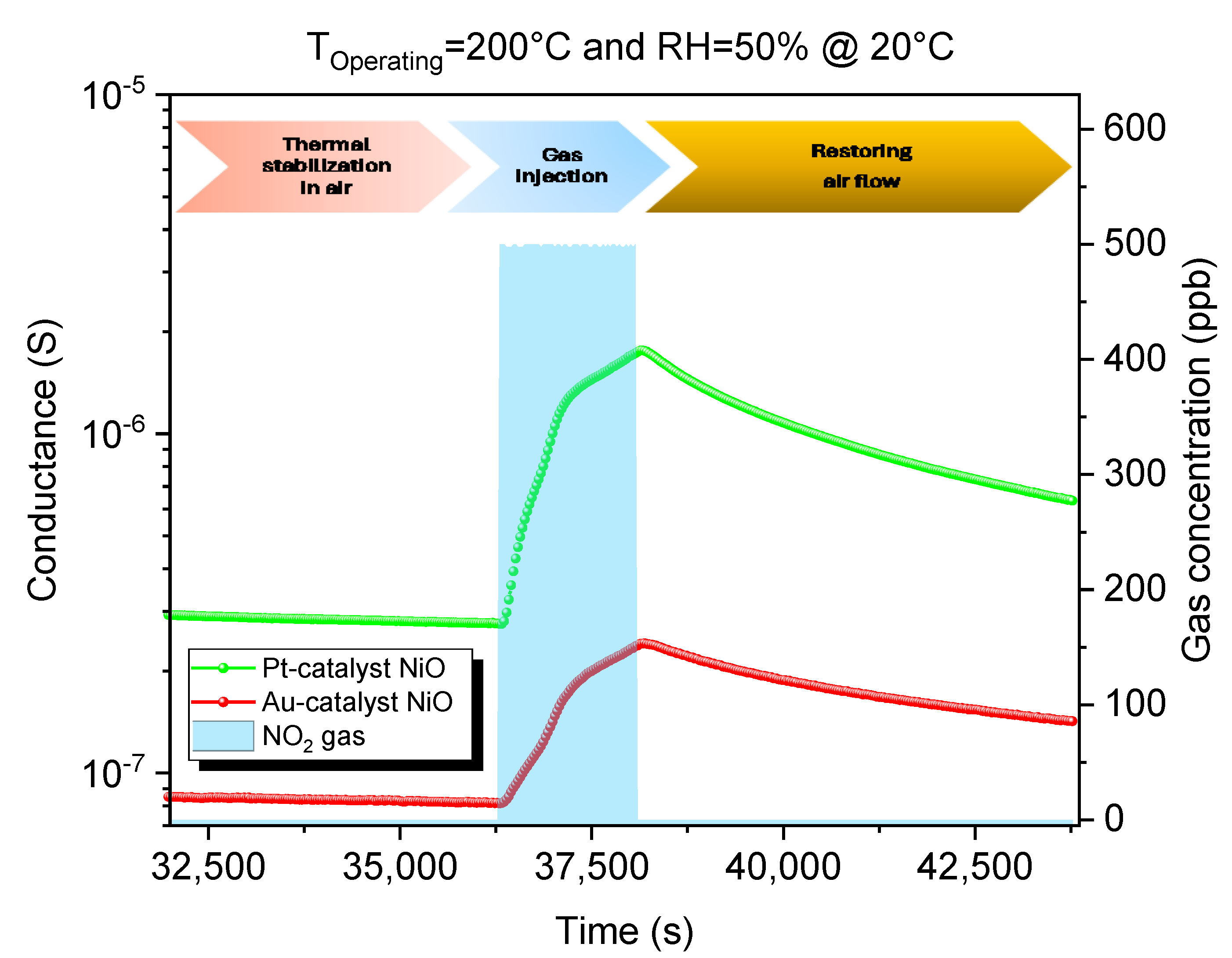
3.2.2. Dynamic Response to NO2

The operational principle of NiO in our gas chamber involves altering the material’s electrical conductance due to variations in free hole density resulting from physisorption, chemisorption, and catalytic reactions between the NiO material’s surface and the target gas. The dynamic curves of Pt catalyst and Au catalyst NiO sensors when exposed to oxidizing gas reflect the p-type characteristic of NiO films, as Figure 8 illustrates.
When exposed to NO2, electrons from the valence band are believed to be trapped at the surface, forming NO 2 species and increasing the hole concentration near the surface, according to reaction (5) [42]:
NO 2 ( g )   NO 2 ( ads ) + h +
Since holes are the majority charge carriers, this significantly boosts the electrical conductivity of the NiO material. NO 2 and molecular/atomic oxygen are two competing species on the NiO adsorption sites, which results in longer recovery transients, as shown in Figure 8, due to the difference in electron affinity (2.3 eV for NO2 and 0.4 eV for molecular oxygen) [43]. Nickel vacancies in NiO significantly enhance its gas-sensing properties with respect to NO2 by creating additional active sites for adsorption, leading to increased sensitivity [44]. These vacancies, often positively charged, facilitate stronger interactions with the electronegative NO2 molecules, resulting in higher adsorption energy and a more pronounced gas response. Furthermore, the vacancies enable efficient electron transfer between the NO2 molecules and the NiO surface, altering the material’s conductivity, which is crucial for detecting gas presence. Additionally, interaction with NO2 can ionize nearby neutral vacancies, further increasing the number of adsorption sites and amplifying the sensor’s effectiveness.

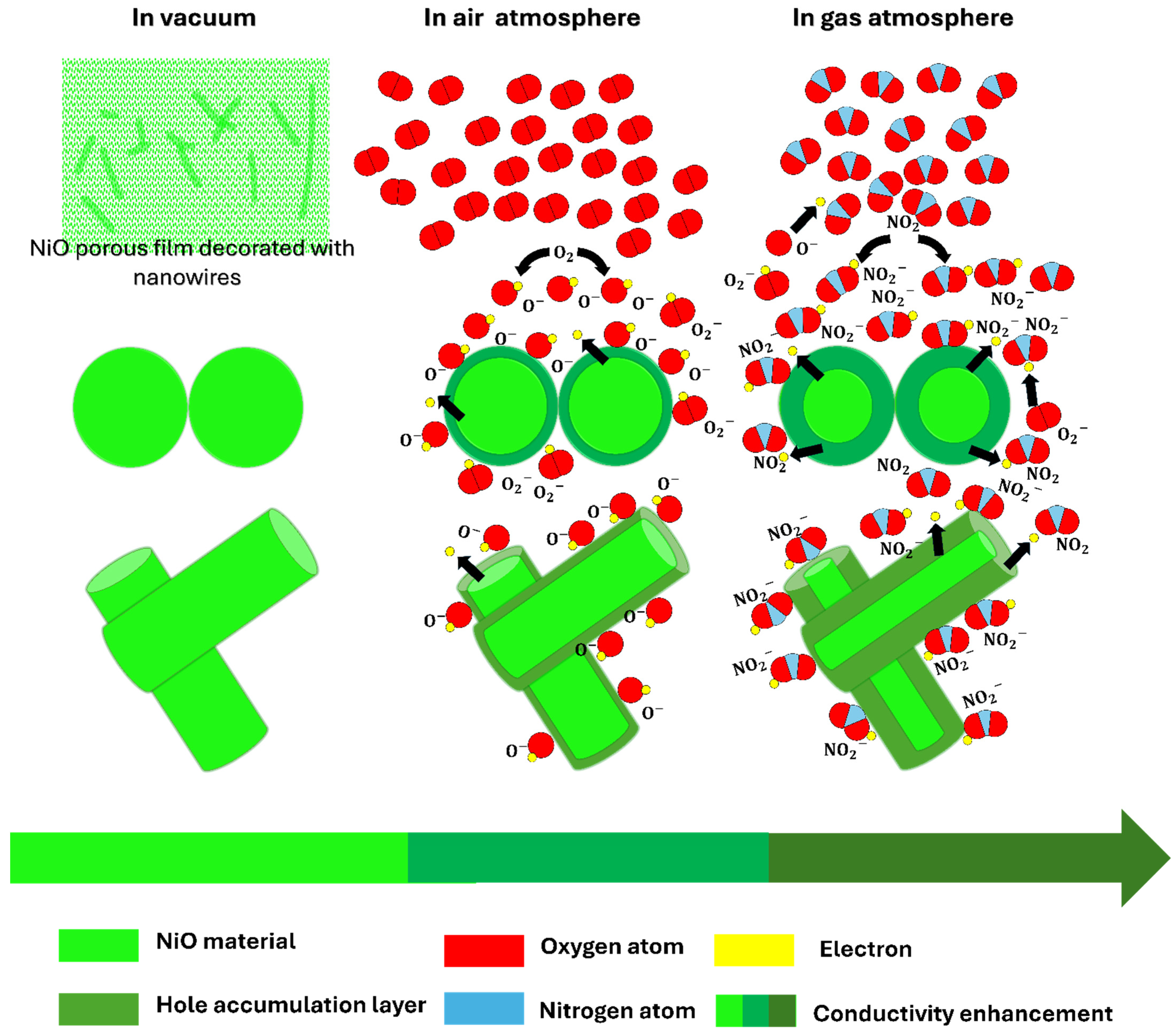
3.2.3. Mechanism of NO2 Sensing

The gas-sensing mechanism of semiconducting NiO gas sensors relies on an alteration in the electrical conductance of the sensing material, where the sensing response will be measured as G = G gas G air G air for oxidizing gas and G = G air G gas G gas for reducing gas. G gas and G air   denote the stable conductance of the sensor in a gas atmosphere and the initial conductance of the sensor in an air atmosphere, respectively.
Upon exposure to air, oxygen molecules adhere to the NiO surface, initiating a process of electron capture from the semiconductor’s conduction band. This leads to the ionosorption of oxygen in molecular form and atomic forms. The presence of these oxygen species depends on the operating temperature.
Upon NO2 exposure, electron capture further increases due to the high electronegativity of the oxidizing molecules, resulting in an increase in the conductance of NiO (rise in hole concentration), characteristic of p-type semiconductors, as presented in Figure 9.
The interaction between NiO and NO2 involves complex surface chemistry, with the type of oxygen species and their reactivity being strongly temperature-dependent.
Low temperatures (<180 °C): Oxygen molecules are weakly adsorbed on the NiO surface and ionized to form O 2 . However, due to insufficient thermal energy, the adsorption and ionization processes are slow, leading to weaker NO2 interaction, a delayed sensor response, and incomplete recovery.
Moderate temperatures (180–400 °C): Molecular oxygen dissociates into atomic oxygen, forming O , which is more reactive than O 2 . The enhanced surface activity increases NO2 adsorption, leading to a significant rise in hole concentration and, consequently, higher sensor sensitivity. The improved interaction between NO2 and O species results in faster and more efficient sensing.
High temperatures (>400 °C): Oxygen species on the NiO surface further ionize into O 2 , increasing surface reactivity. However, the stronger bonds of O 2 may reduce its reactivity toward NO2 compared to O , leading to fewer available active sites. At these temperatures, desorption of reaction products is more efficient, allowing for complete and rapid sensor recovery.
Reactions (6)–(9) describe the oxygen adsorption and surface interaction in different temperature ranges in an air atmosphere [45,46].
O 2 ( gas ) O 2 ( ads )
O 2 ( ads ) + e O 2
O 2 + e 2 O
O + e O 2
After exposure to NO2, the NiO surface reacts with the oxidizing species, according to reactions (10)–(13) [45,47].
NO 2 ( gas ) NO 2 ( ads )
NO 2 ( ads ) + e NO 2
NO 2 ( ads ) + O 2 + 2 e NO 2 + 2 O
NO 2 + 2 O + e NO 2 ( gas ) + 2 O 2
The physisorption of NO2 molecules leads to new acceptor levels, deeper than oxygen levels ( O and O 2 ), which will be chemisorbed ( NO 2 ) and result in band bending at the NiO surface due to the difference in electronegativity. This implies a conductivity increase in the material, as schematized in Figure 9.
Table 2 provides a comprehensive summary of NO2 sensors based on metal oxides synthesized through thermal oxidation, highlighting their key performance metrics.
Table 3 presents a review of the performance of NiO sensors fabricated using various synthesis methods, comparing their sensitivity, operating conditions, and gas-sensing properties.
The NiO sensor developed in this work through thermal oxidation demonstrates a high response (G = 8.65) to 5 ppm of NO2 at 200 °C, outperforming many reported metal oxide sensors and NiO-based sensors synthesized using different methods. Compared to other NO2 sensors in Table 2, our sensor exhibits a significantly higher response at a lower concentration. For instance, ZnO nanorods [51] show a weak response of R = 1.01 to 100 ppm of NO2, while ZnSe/ZnO mesoporous structures [52] achieve a response below 7 for 5 ppm at 200 °C, which is still lower than our sensor.
When compared to NiO sensors synthesized through different methods in Table 3, our sensor maintains a strong advantage. For example, hydrothermally grown NiO nanosheets [57] show an extremely low response (G = 0.39 to 15 ppm of NO2 at room temperature), while NiO nanoparticles prepared via co-precipitation [58] exhibit a response in the range 1.75–2.25 at 180 °C for 5 ppm of NO2, both of which are significantly weaker than our sensor. Even compared to NiO sensors prepared by thermal oxidation, such as the granular film for H2S detection [54] with R′ = 2 at room temperature, our sensor demonstrates a much stronger response, albeit at a slightly higher operating temperature.
In comparison to previous studies on NiO nanowire growth through oxidation, our approach offers greater simplicity and scalability. While studies by Zhu et al. [26], Koga and Hirasawa [29], and others [27,28] rely on advanced techniques such as ESEM, ETEM, and specific starting materials like Ni nanoparticles (NPs), our method utilizes a Ni-sputtered thin film, eliminating the need for complex nanoparticle preparation or in situ monitoring. Moreover, previous studies have not explored the gas-sensing capabilities of NiO nanorods and nanowires, preventing direct performance comparison with thermally oxidized NiO nanowires. However, NiO nanowires synthesized via other methods have shown comparable or even superior NO2-sensing responses. For instance, reference [62] reports that long, thin, and densely packed NiO nanowires (20–60 nm in diameter) exhibited a response of 6 to 1 ppm of NO2 at 200 °C, with an even higher response expected at 5 ppm, surpassing that of Pt-NiO sensors with larger nanowire diameters (~94 nm). Additionally, NiO nanowires grown via the vapor–liquid–solid process demonstrated an impressive response of 54.8 to 1 ppm of NO2 at 200 °C, attributed to their high density and smaller diameters (10–50 nm). These findings highlight the critical role of nanowire morphology in enhancing gas-sensing performance.
The operating temperature plays a crucial role in the recovery of our NiO sensors after exposure to NO2, as shown in Figure 10 and Figure 11. Recovery refers to the sensor’s ability to return to its baseline or initial state after interacting with a specific gas concentration. One can mention the increase in recovery by varying the temperature from 200 °C to 400 °C. Increasing the operating temperature can accelerate the desorption of gas molecules, specifically NO2 species that have high adsorption from the sensor’s surface, leading to a faster recovery time. Higher temperatures provide the necessary energy to break the bonds between the gas molecules and the nickel oxide surface, facilitating a quicker return to baseline readings.
Before exposure to NO2, at lower temperatures, the conductivity of the NiO sensor is relatively low [63]. As the temperature increases, the conductivity of NiO typically increases due to the high concentration and enhanced mobility of free charge carriers within the material. This temperature-dependent conductivity is crucial for the sensor’s operation, as it affects baseline conductance and response characteristics, as mentioned in Figure 11b.
The adsorption of NO2 molecules onto the NiO surface can lead to the transfer of charge between the gas molecules and the Ni vacancies. This charge transfer process results in altering the conductivity of the NiO sensor via following the reactions (14)–(16) [41].
NO 2 ( gas ) NO 2 ( ads )
NO 2 ( ads ) + V N i NO 2 ( ads ) + V N i
V N i V N i + h +
At an optimum temperature, the sensor exhibits the highest response to NO2, as an equilibrium between the adsorption and desorption kinetics of NO2 molecules is achieved. It is worth noting that high temperatures can affect the thermal stability of Ni vacancies. If the temperature exceeds a certain threshold, it could lead to the recombination of vacancies with other defects or atoms, reducing the number of available active sites and potentially decreasing the sensor’s responsiveness, as described in Figure 10f.
The desorption of NO2 molecules from the NiO surface occurs, leading to a decrease in the concentration of surface adsorption sites and a restoration of the sensor’s baseline conductance. The desorption rate is also temperature dependent: it increases with higher temperatures, facilitating faster desorption kinetics. At lower temperatures, a higher proportion of NO2 adsorption may be irreversible, meaning that some NO2 molecules form strong and potentially permanent bonds with the sensor surface. The recovery time after exposure to NO2 was notably lengthy for Au-NiO and Pt-NiO sensors, taking hours, resulting in subsequent gas exposures occurring before the sensors had fully recovered. This prolonged recovery time for NO2 is a common observation in terms of NiO-based sensors.
At higher temperatures, the adsorption process is more reversible, allowing the sensor to fully recover after NO2 exposure. Those implications are proved in Figure 11a,b by describing the recovery rate and the baseline conductance at different operating temperatures, showing higher recovery and higher conductance by increasing the temperature from 200 °C to 400 °C.
The NiO sensors demonstrated good reproducibility after undergoing two cyclic measurements (1 ppm) at the optimum condition (See Figure 12). During air injection into the gas chamber, the sensors cannot return to their initial baseline, as seen in Figure 12a. This behavior is due to the high binding energy of NO2 molecules, which can be addressed by thermal activation, as shown in Figure 10, optical excitation, and formation of heterojunctions, which provide fresh active sites and enhance adsorption–desorption rates [64].

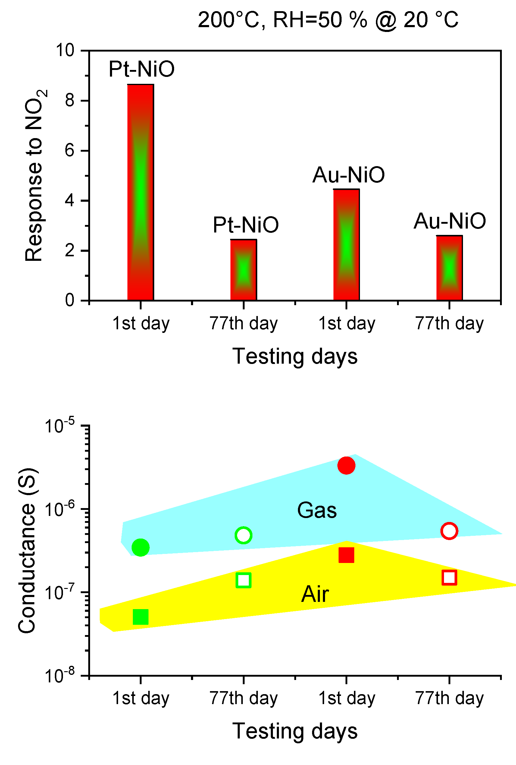
3.2.4. Moisture Effect

Cross-interference with humidity significantly limits the reliability and accuracy of gas detection in metal oxide gas sensors. In humid environments, water molecules readily deactivate the active sites on the surface of metal oxides that are crucial for gas adsorption, hence limiting their gas response. P-type semiconductors are known for their low humidity dependency. However, NiO sensors show better sensing performance in humid air, unlike dry air. In Figure 13, we exhibit the dynamic curves in dry air under exposure to NO2 and the response toward various gas concentrations in dry and wet environments to study the effect of humidity on the sensing performance of NiO samples. One can see that humid environments show a higher response compared to dry environments for Au- and Pt-NiO sensors. Similar observations are made for silicon dioxide as a p-type material, which is more tolerant to moisture under exposure to NO2 [65]: NO2 has a stronger interaction with the surface compared to water and oxygen molecules, making it the most favorable reactant. The gas response of the SiO2 sensor to 0.2 ppm of NO2 is enhanced in humid air (RH = 50%), with an average increase of 30% compared to the response in dry air (RH = 0%). A higher increase in NiO responsiveness is recorded for Pt-NiO (×2700%) and Au-NiO (×400%) sensors when changing the environment from dry to humid under exposure to 1 ppm of NO2 (See Figure 13c).
Following the conventional power law for gas response G = α . c n applicable to metal oxides for gas-sensing applications and the 100% method (to achieve a minimum response of 1), we calculate the limit of detections LOD = 26 ppb and LOD = 0.2 ppb for Au-NiO and Pt-NiO sensors, respectively, based on the calibration presented in Figure 14. The parameters α , c , and n are indicative of the sensitivity parameter (ppm−1), the gas concentration of nitrogen dioxide (ppm), and the surface reaction kinetics between NO2 molecules and the predominant oxygen species at 200 °C.
Breathing high levels of NO2 can irritate the respiratory system and worsen conditions like asthma. The Occupational Safety and Health Administration (OSHA) provides permissible exposure limits (PELs) for NO2 in the workplace. According to OSHA, the PEL for NO2 is 5 ppm as a ceiling limit, which should not be exceeded during any part of the working day. Another organization, the National Institute for Occupational Safety and Health (NIOSH), recommends 1 ppm and 40 ppb as short-term exposure limits (STPELs) at 1 h and 24 h, respectively. Our sensors have an exceptionally low limit of detection, capable of identifying NO2 concentrations as low as 0.2 to 26 ppb. This sensitivity allows the NiO sensors to detect NO2 at levels significantly below the short-term exposure limits set by both OSHA and NIOSH. This ensures high safety and effective monitoring, providing protection well beyond the recommended exposure limits for nitric acid gas. However, at optimal conditions, NiO sensors show incomplete recovery due to the high binding energy of NO2 molecules on the sensor surface. At a higher operating temperature of 400 °C, the sensors achieve full recovery, yet the response is reduced compared to 200 °C. Specifically, for Pt-NiO sensors, the response at 200 °C is 12.72 times that at 400 °C, and for Au-NiO, it is 4.28 times greater at 200 °C than at 400 °C. Thus, while elevated temperatures can improve recovery, they reduce sensor response, highlighting a trade-off between sensitivity and recovery efficiency.
Additional critical measurements, such as selectivity and stability, are conducted to validate the overall sensing performance of NiO sensors. In Figure 15, we measured sensitivity and selectivity under identical operating conditions toward various analytes: NO2, NH3, acetone, toluene, H2, and CO.
A closer look at the bar chart shown in Figure 15b can justify the response of the sensors toward reducing and oxidizing gases: high NO2 selectivity is associated with the lowest dissociation-bond energy for O NO among the other gases’ energies. The high electronegativity of NO2 molecules also explains the highest response compared to the response relative to the reducing gases. Wang et al., using DFT calculations, determined the adsorption energies of NO2 and NH3 on the NiO surface [68]. They found that the interaction between NO2 molecules and the NiO surface was the strongest. For instance, when comparing NO2 to NH3 gas, we find that the oxidizing gas has lower adsorption energy ( E ads NO 2 = 0.310   eV / molecule vs. E ads NH 3 = 0.101   eV / molecule [68]), which implies stronger binding to the surface, higher adsorption, and better sensing response. Complementary in situ DRIFT studies by Zhang et al. revealed that a higher number of nickel vacancies in NiO nanostructures enhanced their sensitivity to NO2 [69]. They realized that the strong interaction between doubly charged nickel vacancies and NO2 species through electron transfer promoted the ionization of neutral nickel vacancies, thereby creating more adsorption sites for the analyte and enhancing the sensing property. The adsorption energy also accounts for the gas response to 50 ppm of CO and hydrogen gases, where the CO response (18.40%) is higher than that of H2 (4.75%). This difference can be attributed to the lower adsorption energy of CO on the NiO surface, as calculated by Nie et al., with E ads CO = 1.496   eV compared to E ads H 2 = 0.146   eV [70].
Regarding the long-term stability protocol, the measurements were conducted over a period of 77 days, as shown in Figure 16. These were not continuous but rather taken at selected intervals to assess sensor stability over time. The response decrease toward NO2 by three orders for Pt-NiO sensors can be addressed in terms of the possible remaining gas on the active sites of NiO after tens of cyclic measurements in succession, noting that the initial conductance in air, described in Figure 16, increases on the 77th day, compared to the first day (high surface conductivity may be explained by the presence of NO2 molecules on the surface as they have strong affinity and adsorption energy).
Wang et al. demonstrated, via molecular simulation, that NO2 has strong interaction on NiO surfaces, leading to the formation of additional adsorption monolayers of the oxidizing gas, which saturate the reactive sites and make it challenging to completely remove the gas species from the surface, resulting in a lower sensing response [68]. Another factor to consider when working with p-type materials is the Mars–van Krevelen mechanism [46]: the reactivity of lattice oxygen can significantly impact the sensing performance of metal oxides over time. The surface lattice oxygen is more prone to losing electrons to bulk oxygen, thereby becoming reactive and participating in surface reactions. Over time, this loss of lattice oxygen could explain the observed decline in the performance of p-type materials, such as the drastic decrease in the sensitivity of NiO sensors over 77 days.

4. Conclusions

In conclusion, this study has successfully demonstrated a straightforward and cost-effective method for fabricating porous NiO films decorated with nanowires, achieved through sputtering followed by thermal oxidation of the Ni layer with two thicknesses using different catalysis. The structural analysis confirmed the presence of a single NiO phase and the formation of nanowires within the porous matrix. Our investigation into the gas-sensing properties of these films, particularly towards NO2, highlighted the superior performance of thinner layers with the Pt catalyst at an optimal operating temperature of 200 °C, albeit with incomplete recovery due to the strong binding energy of NO2 molecules. While higher temperatures facilitated full recovery, this came at the cost of reduced sensor responsiveness. Additionally, the study explored the significant impact of moisture in terms of enhancing the responsiveness of Pt-NiO and Au-NiO sensors. The higher sensor response in humid conditions compared to dry air is attributed to the displacement of pre-existing water on the surface by NO2 molecules. The findings underscore the potential of this simple fabrication approach for producing NiO nanowires, offering a promising and scalable alternative for applications in gas sensing and beyond. Nonetheless, over repeated cycles, the response of the NiO sensors toward NO2 decreases, which can be attributed to residual gas molecules that may remain on NiO’s active sites after successive measurements. This decline is also reflected in the increase in initial conductance in air by the 11th week compared to the first day, suggesting that NO2 molecules with high adsorption energy remain partially adsorbed on the surface, contributing to a persistent high surface conductivity. This effect highlights the critical trade-offs in long-term sensor reliability, where maintaining high response and recovery over extended use remains challenging for gas monitoring.

Author Contributions

Conceptualization, M.B.A.; methodology, M.B.A.; validation, E.C.; formal analysis, M.B.A.; investigation, M.B.A.; resources, E.C. and J.-B.Y.; data curation, M.B.A.; writing—original draft preparation, M.B.A.; writing—review and editing, M.B.A., E.C., S.-H.K. and J.-B.Y.; visualization, M.B.A.; supervision, E.C.; project administration, E.C.; funding acquisition, E.C. and J.-B.Y. All authors have read and agreed to the published version of the manuscript.

Funding

This research was funded in part by the Italian Ministry of Foreign Affairs and International Cooperation, grant number KR23GR02.

Institutional Review Board Statement

Not applicable. This study does not involve humans or animals.

Informed Consent Statement

Not applicable. This study does not involve human subjects.

Data Availability Statement

The original contributions presented in this study are included in the article. Further inquiries can be directed to the corresponding author.

Conflicts of Interest

The authors declare no conflicts of interest.

References

  1. Cao, L.; Yu, L.; Li, S.; Nan, N.; Zhang, C.; Fan, X. In-situ growth of well-ordered ZnO nanowire-networks with interconnected junctions for enhanced SO2 gas sensing properties. Appl. Surf. Sci. 2024, 646, 158899. [Google Scholar] [CrossRef]
  2. Tonezzer, M. Selective gas sensor based on one single SnO2 nanowire. Sens. Actuators B Chem. 2019, 288, 53–59. [Google Scholar] [CrossRef]
  3. Tonezzer, M.; Hieu, N.V. Size-dependent response of single-nanowire gas sensors. Sens. Actuators B Chem. 2012, 163, 146–152. [Google Scholar] [CrossRef]
  4. Vallejos, S.; Di Maggio, F.; Shujah, T.; Blackman, C. Chemical vapour deposition of gas sensitive metal oxides. Chemosensors 2016, 4, 4. [Google Scholar] [CrossRef]
  5. Chen, L.; Yu, Q.; Pan, C.; Song, Y.; Dong, H.; Xie, X.; Li, Y.; Liu, J.; Wang, D.; Chen, X. Chemiresistive gas sensors based on electrospun semiconductor metal oxides: A review. Talanta 2022, 246, 123527. [Google Scholar] [CrossRef]
  6. Li, R.; Chen, S.; Lou, Z.; Li, L.; Huang, T.; Song, Y.; Chen, D.; Shen, G. Fabrication of porous SnO2 nanowires gas sensors with enhanced sensitivity. Sens. Actuators B Chem. 2017, 252, 79–85. [Google Scholar] [CrossRef]
  7. Dang, T.T.L.; Tonezzer, M.; Nguyen, V.H. Hydrothermal growth and hydrogen selective sensing of nickel oxide nanowires. J. Nanomater. 2015, 2015, 785856. [Google Scholar] [CrossRef]
  8. Ramgir, N.; Datta, N.; Kaur, M.; Kailasaganapathi, S.; Debnath, A.K.; Aswal, D.; Gupta, S. Metal oxide nanowires for chemiresistive gas sensors: Issues, challenges and prospects. Colloids Surf. A Physicochem. Eng. Asp. 2013, 439, 101–116. [Google Scholar] [CrossRef]
  9. Kaur, N.; Comini, E.; Zappa, D.; Poli, N.; Sberveglieri, G. Nickel oxide nanowires: Vapor liquid solid synthesis and integration into a gas sensing device. Nanotechnology 2016, 27, 205701. [Google Scholar] [CrossRef]
  10. Supab, C.; Niyom, H.; Ekasiddh, W. Metal-Oxide Nanowires by Thermal Oxidation Reaction Technique. In Nanowires; Paola, P., Ed.; IntechOpen: Rijeka, Croatia, 2010; Chapter 5. [Google Scholar]
  11. Zappa, D.; Briand, D.; Comini, E.; Courbat, J.; De Rooij, N.; Sberveglieri, G. Zinc oxide nanowires deposited on polymeric hotplates for low-power gas sensors. Procedia Eng. 2012, 47, 1137–1140. [Google Scholar] [CrossRef]
  12. Spanu, D.; Recchia, S.; Schmuki, P.; Altomare, M. Thermal-Oxidative Growth of Substoichiometric WO3−x Nanowires at Mild Conditions. Phys. Status Solidi (RRL)–Rapid Res. Lett. 2020, 14, 2000235. [Google Scholar]
  13. Zappa, D.; Comini, E.; Zamani, R.; Arbiol, J.; Morante, J.; Sberveglieri, G. Copper oxide nanowires prepared by thermal oxidation for chemical sensing. Procedia Eng. 2011, 25, 753–756. [Google Scholar]
  14. Zappa, D.; Bertuna, A.; Comini, E.; Molinari, M.; Poli, N.; Sberveglieri, G. Tungsten oxide nanowires for chemical detection. Anal. Methods 2015, 7, 2203–2209. [Google Scholar]
  15. Zappa, D.; Comini, E.; Zamani, R.; Arbiol, J.; Morante, J.; Sberveglieri, G. Preparation of copper oxide nanowire-based conductometric chemical sensors. Sens. Actuators B Chem. 2013, 182, 7–15. [Google Scholar]
  16. Munasinghe Arachchige, H.M.; Zappa, D.; Poli, N.; Gunawardhana, N.; Attanayake, N.H.; Comini, E. Seed-assisted growth of TiO2 nanowires by thermal oxidation for chemical gas sensing. Nanomaterials 2020, 10, 935. [Google Scholar] [CrossRef]
  17. Moumen, A.; Kumarage, G.C.W.; Comini, E. P-Type Metal Oxide Semiconductor Thin Films: Synthesis and Chemical Sensor Applications. Sensors 2022, 22, 1359. [Google Scholar] [CrossRef]
  18. Ren, Y.; Chiam, S.; Chim, W. Diameter dependence of the void formation in the oxidation of nickel nanowires. Nanotechnology 2011, 22, 235606. [Google Scholar]
  19. Xiang, W.; Dong, Z.; Luo, Y.; Zhao, J.; Wang, J.-o.; Ibrahim, K.; Zhan, H.; Yue, W.; Guo, H. Synthesis of NiO Nanotubes via a Dynamic Thermal Oxidation Process. Materials 2019, 12, 805. [Google Scholar] [CrossRef]
  20. Zhang, J.; Xiang, W.; Liu, Y.; Hu, M.; Zhao, K. Synthesis of High-Aspect-Ratio Nickel Nanowires by Dropping Method. Nanoscale Res. Lett. 2016, 11, 118. [Google Scholar] [CrossRef]
  21. Hajakbari, F. Characterization of nanocrystalline nickel oxide thin films prepared at different thermal oxidation temperatures. J. Nanostruct. Chem. 2020, 10, 97–103. [Google Scholar] [CrossRef]
  22. Ravikumar, P.; Taparia, D.; Alagarsamy, P. Thickness-Dependent Thermal Oxidation of Ni into NiO Thin Films. J. Supercond. Nov. Magn. 2018, 31, 3761–3775. [Google Scholar] [CrossRef]
  23. Abubakar, D.; Ahmed, N.M.; Mahmud, S.; Algadri, N.A. Properties of NiO nanostructured growth using thermal dry oxidation of nickel metal thin film for hydrogen gas sensing at room temperature. Mater. Res. Express 2017, 4, 075009. [Google Scholar] [CrossRef]
  24. Raghavan, L.; Ojha, S.; Sulania, I.; Mishra, N.C.; Ranjith, K.M.; Baenitz, M.; Kanjilal, D. Thermal annealing induced competition of oxidation and grain growth in nickel thin films. Thin Solid Film. 2019, 680, 40–47. [Google Scholar] [CrossRef]
  25. Unutulmazsoy, Y.; Merkle, R.; Fischer, D.; Mannhart, J.; Maier, J. The oxidation kinetics of thin nickel films between 250 and 500 °C. Phys. Chem. Chem. Phys. 2017, 19, 9045–9052. [Google Scholar] [CrossRef]
  26. Zhu, W.; Winterstein, J.P.; Sharma, R.; Zhou, G. The Growth of Catalyst-free NiO Nanowires. Microsc. Microanal. 2016, 22, 1620–1621. [Google Scholar]
  27. Qu, B.; van Benthem, K. In situ anisotropic NiO nanostructure growth at high temperature and under water vapor. J. Am. Ceram. Soc. 2022, 105, 2454–2464. [Google Scholar] [CrossRef]
  28. Qu, B.; van Benthem, K. In-situ anisotropic growth of nickel oxide nanostructures through layer-by-layer metal oxidation. Scr. Mater. 2022, 214, 114660. [Google Scholar] [CrossRef]
  29. Koga, K.; Hirasawa, M. Anisotropic growth of NiO nanorods from Ni nanoparticles by rapid thermal oxidation. Nanotechnology 2013, 24, 375602. [Google Scholar] [CrossRef]
  30. Xiang, L.; Guo, J.; Wu, C.; Cai, M.; Zhou, X.; Zhang, N. A brief review on the growth mechanism of CuO nanowires via thermal oxidation. J. Mater. Res. 2018, 33, 2264–2280. [Google Scholar] [CrossRef]
  31. Ponzoni, A. Metal Oxide Chemiresistors: A Structural and Functional Comparison between Nanowires and Nanoparticles. Sensors 2022, 22, 3351. [Google Scholar] [CrossRef]
  32. Shooshtari, M.; Salehi, A. An electronic nose based on carbon nanotube -titanium dioxide hybrid nanostructures for detection and discrimination of volatile organic compounds. Sens. Actuators B Chem. 2022, 357, 131418. [Google Scholar] [CrossRef]
  33. Shooshtari, M.; Salehi, A.; Vollebregt, S. Effect of temperature and humidity on the sensing performance of TiO2 nanowire-based ethanol vapor sensors. Nanotechnology 2021, 32, 325501. [Google Scholar] [CrossRef] [PubMed]
  34. Chen, H.-L.; Yang, Y.-S. Effect of crystallographic orientations on electrical properties of sputter-deposited nickel oxide thin films. Thin Solid Film. 2008, 516, 5590–5596. [Google Scholar] [CrossRef]
  35. Penza, M.; Cassano, G.; Rossi, R.; Alvisi, M.; Rizzo, A.; Signore, M.A.; Dikonimos, T.; Serra, E.; Giorgi, R. Enhancement of sensitivity in gas chemiresistors based on carbon nanotube surface functionalized with noble metal (Au, Pt) nanoclusters. Appl. Phys. Lett. 2007, 90, 173123. [Google Scholar] [CrossRef]
  36. Kim, J.; Park, W.H.; Doh, W.H.; Lee, S.W.; Noh, M.C.; Gallet, J.-J.; Bournel, F.; Kondoh, H.; Mase, K.; Jung, Y. Adsorbate-driven reactive interfacial Pt-NiO1−x nanostructure formation on the Pt3Ni (111) alloy surface. Sci. Adv. 2018, 4, eaat3151. [Google Scholar] [CrossRef]
  37. Nikolaev, S.; Pichugina, D.; Mukhamedzyanova, D. Sites for the selective hydrogenation of ethyne to ethene on supported NiO/Au catalysts. Gold Bull. 2012, 45, 221–231. [Google Scholar] [CrossRef]
  38. Burns, A.R.; Jennison, D.R.; Stechel, E.B. Electronically stimulated dissociation of NO2 on Pt(111). Phys. Rev. B Condens. Matter. 1989, 40, 9485–9497. [Google Scholar] [CrossRef]
  39. Yuan, Z.; Zhang, S.; Meng, F.; Zhang, H.; Zuo, K. Investigation of grain radius dependence of sensitivity for porous thin film semiconducting metal oxide gas sensor. IEEE Sens. J. 2019, 20, 4275–4282. [Google Scholar] [CrossRef]
  40. Gomaa, M.M.; Sayed, M.H.; Patil, V.L.; Boshta, M.; Patil, P.S. Gas sensing performance of sprayed NiO thin films toward NO2 gas. J. Alloys Compd. 2021, 885, 160908. [Google Scholar] [CrossRef]
  41. Mokoena, T.P.; Swart, H.C.; Motaung, D.E. A review on recent progress of p-type nickel oxide based gas sensors: Future perspectives. J. Alloys Compd. 2019, 805, 267–294. [Google Scholar] [CrossRef]
  42. Park, S.; Kim, S.; Kheel, H.; Lee, C. Oxidizing gas sensing properties of the n-ZnO/p-Co3O4 composite nanoparticle network sensor. Sens. Actuators B Chem. 2016, 222, 1193–1200. [Google Scholar] [CrossRef]
  43. Wilson, R.L.; Simion, C.E.; Stanoiu, A.; Taylor, A.; Guldin, S.; Covington, J.A.; Carmalt, C.J.; Blackman, C.S. Humidity-Tolerant Ultrathin NiO Gas-Sensing Films. ACS Sens. 2020, 5, 1389–1397. [Google Scholar] [CrossRef] [PubMed]
  44. Zhang, J.; Hu, D.; Tian, S.; Qin, Z.; Zeng, D.; Xie, C. CuInS2 QDs decorated ring-like NiO for significantly enhanced room-temperature NO2 sensing performances via effective interfacial charge transfer. Sens. Actuators B Chem. 2018, 256, 1001–1010. [Google Scholar] [CrossRef]
  45. Gawali, S.R.; Patil, V.L.; Deonikar, V.G.; Patil, S.S.; Patil, D.R.; Patil, P.S.; Pant, J. Ce doped NiO nanoparticles as selective NO2 gas sensor. J. Phys. Chem. Solids 2018, 114, 28–35. [Google Scholar] [CrossRef]
  46. Walker, J.M.; Akbar, S.A.; Morris, P.A. Synergistic effects in gas sensing semiconducting oxide nano-heterostructures: A review. Sens. Actuators B Chem. 2019, 286, 624–640. [Google Scholar] [CrossRef]
  47. Pakdel, H.; Borsi, M.; Ponzoni, M.; Comini, E. Enhanced Gas Sensing Performance of CuO-ZnO Composite Nanostructures for Low-Concentration NO2 Detection. Chemosensors 2024, 12, 54. [Google Scholar] [CrossRef]
  48. Behera, B.; Chandra, S. Synthesis of WO3 nanorods by thermal oxidation technique for NO2 gas sensing application. Mater. Sci. Semicond. Process. 2018, 86, 79–84. [Google Scholar] [CrossRef]
  49. Han, T.-H.; Bak, S.-Y.; Kim, S.; Lee, S.H.; Han, Y.-J.; Yi, M. Decoration of CuO NWs Gas Sensor with ZnO NPs for Improving NO2 Sensing Characteristics. Sensors 2021, 21, 2103. [Google Scholar] [CrossRef]
  50. Hou, J.-L.; Lin, Y.-T.; Hsueh, T.-J. Employing Thermal Oxidation and Through-Silicon Via Technologies in CuO-Based Sensors for Room-Temperature NO2 Detection. J. Electrochem. Soc. 2024, 171, 057512. [Google Scholar] [CrossRef]
  51. Navale, Y.H.; Navale, S.T.; Ramgir, N.S.; Stadler, F.J.; Gupta, S.K.; Aswal, D.K.; Patil, V.B. Zinc oxide hierarchical nanostructures as potential NO2 sensors. Sens. Actuators B Chem. 2017, 251, 551–563. [Google Scholar] [CrossRef]
  52. Liu, W.; Gu, D.; Li, X. Ultrasensitive NO2 Detection Utilizing Mesoporous ZnSe/ZnO Heterojunction-Based Chemiresistive-Type Sensors. ACS Appl. Mater. Interfaces 2019, 11, 29029–29040. [Google Scholar] [CrossRef]
  53. Hou, J.-L.; Lin, Y.-T.; Hsueh, T.-J. Room-Temperature TiO2 Gas Sensor with Conical-TSV Using a Thermal Oxidation Process. ACS Appl. Electron. Mater. 2023, 5, 6542–6548. [Google Scholar] [CrossRef]
  54. Dastan, D.; Shan, K.; Jafari, A.; Marszalek, T.; Mohammed, M.K.A.; Tao, L.; Shi, Z.; Chen, Y.; Yin, X.-T.; Alharbi, N.D.; et al. Influence of heat treatment on H2S gas sensing features of NiO thin films deposited via thermal evaporation technique. Mater. Sci. Semicond. Process. 2023, 154, 107232. [Google Scholar] [CrossRef]
  55. Nakate, U.T.; Ahmad, R.; Patil, P.; Yu, Y.T.; Hahn, Y.-B. Ultra thin NiO nanosheets for high performance hydrogen gas sensor device. Appl. Surf. Sci. 2020, 506, 144971. [Google Scholar] [CrossRef]
  56. Baek, J.; Kim, Y.; Baik, K.H.; Jang, S. H2S Sensing Characteristics of NiO Nanopetal Film. ECS J. Solid. State Sci. Technol. 2023, 12, 085002. [Google Scholar] [CrossRef]
  57. Zhang, J.; Zeng, D.; Zhao, S.; Wu, J.; Xu, K.; Zhu, Q.; Zhang, G.; Xie, C. Room temperature NO2 sensing: What advantage does the rGO-NiO nanocomposite have over pristine NiO? Phys. Chem. Chem. Phys. 2015, 17, 14903–14911. [Google Scholar] [CrossRef]
  58. Sharma, P.; Kumar, S.; Vishwanadh, B.; Girija, K.G. Cost-effective synthesis of NiO nanoparticles and realization of highly selective NO2 sensors. Appl. Phys. A 2022, 128, 630. [Google Scholar] [CrossRef]
  59. Chou, P.-C.; Chen, H.-I.; Liu, I.P.; Chen, C.-C.; Liou, J.-K.; Hsu, K.-S.; Liu, W.-C. Hydrogen sensing performance of a nickel oxide (NiO) thin film-based device. Int. J. Hydrogen Energy 2015, 40, 729–734. [Google Scholar] [CrossRef]
  60. Chou, P.-C.; Chen, H.-I.; Liu, I.-P.; Chen, C.-C.; Liou, J.-K.; Hsu, K.-S.; Liu, W.-C. On the ammonia gas sensing performance of a RF sputtered NiO thin-film sensor. IEEE Sens. J. 2015, 15, 3711–3715. [Google Scholar]
  61. Prajesh, R.; Goyal, V.; Nahid, M.; Saini, V.; Singh, A.K.; Sharma, A.K.; Bhargava, J.; Agarwal, A. Nickel oxide (NiO) thin film optimization by reactive sputtering for highly sensitive formaldehyde sensing. Sens. Actuators B Chem. 2020, 318, 128166. [Google Scholar] [CrossRef]
  62. Zappa, D.; Bertuna, A.; Comini, E.; Kaur, N.; Poli, N.; Sberveglieri, V.; Sberveglieri, G. Metal oxide nanostructures: Preparation, characterization and functional applications as chemical sensors. Beilstein J. Nanotechnol. 2017, 8, 1205–1217. [Google Scholar] [CrossRef]
  63. Osburn, C.M.; Vest, R.W. Defect structure and electrical properties of NiO—I. High temperature. J. Phys. Chem. Solids 1971, 32, 1331–1342. [Google Scholar] [CrossRef]
  64. Agrawal, A.V.; Kumar, N.; Kumar, M. Strategy and Future Prospects to Develop Room-Temperature-Recoverable NO2 Gas Sensor Based on Two-Dimensional Molybdenum Disulfide. Nano-Micro Lett. 2021, 13, 38. [Google Scholar] [CrossRef]
  65. Brophy, R.E.; Junker, B.; Fakhri, E.A.; Árnason, H.Ö.; Svavarsson, H.G.; Weimar, U.; Bârsan, N.; Manolescu, A. Ultra Responsive NO2 silicon nanowires gas sensor. Sens. Actuators B Chem. 2024, 410, 135648. [Google Scholar] [CrossRef]
  66. Tit, N.; Said, K.; Mahmoud, N.M.; Kouser, S.; Yamani, Z.H. Ab-initio investigation of adsorption of CO and CO2 molecules on graphene: Role of intrinsic defects on gas sensing. Appl. Surf. Sci. 2017, 394, 219–230. [Google Scholar] [CrossRef]
  67. Bang, J.H.; Choi, M.S.; Mirzaei, A.; Kwon, Y.J.; Kim, S.S.; Kim, T.W.; Kim, H.W. Selective NO2 sensor based on Bi2O3 branched SnO2 nanowires. Sens. Actuators B Chem. 2018, 274, 356–369. [Google Scholar] [CrossRef]
  68. Wang, B.; Nisar, J.; Ahuja, R. Molecular Simulation for Gas Adsorption at NiO (100) Surface. ACS Appl. Mater. Interfaces 2012, 4, 5691–5697. [Google Scholar] [CrossRef]
  69. Zhang, J.; Zeng, D.; Zhu, Q.; Wu, J.; Huang, Q.; Xie, C. Effect of Nickel Vacancies on the Room-Temperature NO2 Sensing Properties of Mesoporous NiO Nanosheets. J. Phys. Chem. C 2016, 120, 3936–3945. [Google Scholar] [CrossRef]
  70. Nie, S.; Li, J.; He, Y.; Yin, X. Selective adsorption behavior of reducing gases on the NiO–In2O3 heterojunction under the interfacial effect. Ceram. Int. 2024, 50, 41397–41406. [Google Scholar] [CrossRef]
Figure 1. Sketch of NiO sensor preparation at the sensor laboratory.
Sensors 25 02075 g001
Figure 2. SEM images of (a,b) Pt-NiO and (c,d) Au-NiO structures oxidized at 800 °C.
Sensors 25 02075 g002
Figure 3. Representation of the Ni film oxidation process.
Sensors 25 02075 g003
Figure 4. (a,c) Length distribution and (b,d) diameter distribution of nanowires for Au-NiO and Pt-NiO with a thickness of 200 nm.
Sensors 25 02075 g004
Figure 5. GIXRD patterns of Pt-NiO film (450 nm) oxidized at 800 °C for 4 h.
Sensors 25 02075 g005
Figure 6. EDX analysis of the Pt-NiO (200 nm) sample.
Sensors 25 02075 g006
Figure 7. Dependency of NO2 response on an operating temperature of RH = 50% @ 20 °C for different NiO sensors.
Sensors 25 02075 g007
Figure 8. Dynamic response curves with respect to 0.5 ppm NO2 at 200 °C and RH = 50% @ 20 °C for Au catalyst NiO sensors.
Sensors 25 02075 g008
Figure 9. Schematic description of gas-sensing mechanisms.
Sensors 25 02075 g009
Figure 10. Dynamic response–recovery curves of Au catalyst and Pt catalyst NiO sensors with respect to 5 ppm of NO2 at different working temperatures: (a) 200 °C, (b) 250 °C, (c) 300 °C, (d) 350 °C, and (e) 400 °C, with (f) temperature dependency in terms of their gas response and recovery rate at 50% of relative humidity. The yellow and blue areas indicate the recovery time for Pt-NiO and Au-NiO sensors, respectively. The green and red bars represent the response intensity of Pt-NiO and Au-NiO sensors, respectively. The yellow and blue lines correspond to the recovery characteristics of the Pt-NiO and Au-NiO sensors, respectively.
Sensors 25 02075 g010
Figure 11. (a) Histogram representation of recovery versus operating temperature at 50% of relative humidity, and (b) temperature-dependent baseline conductance for Au- and Pt-NiO sensors.
Sensors 25 02075 g011
Figure 12. (a) Dynamic response–recovery curves of Au-NiO and Pt-NiO sensors under exposure to NO2 at different concentrations at 200 °C and 50% of relative humidity. (b) is the histogram representation of NO2 response for both sensors.
Sensors 25 02075 g012
Figure 13. (a) Dynamic response–recovery curves of Au catalyst and Pt catalyst NiO sensors under exposure to NO2 at different concentrations at 200 °C in a dry atmosphere. (b,c) are the histogram representations of NO2 response in dry and humid environments and the humidity-to-dryness response ratio for both sensors. (d) represents the initial baseline conductance before exposure to gas for the sensors in dry and humid atmospheres.
Sensors 25 02075 g013
Figure 14. Calibration of NiO sensors with a thickness of 200 nm in optimum conditions.
Sensors 25 02075 g014
Figure 15. (a) Gas selectivity to nitrogen dioxide, ammonia, acetone, toluene, hydrogen, and carbon monoxide at the optimum operating temperature. (b) dissociation bond energies of each tested gas [47,66,67].
Sensors 25 02075 g015
Figure 16. Long-term stability of NiO sensors: response to NO2 and initial conductance in air and gas over 77 days. The green and red shapes indicate the conductance of Pt-NiO and Au-NiO sensors, respectively.
Sensors 25 02075 g016
Table 1. XRD parameters corresponding to the (200) crystallographic plane of NiO.
ParameterValue
θ (degree)43.38
2 θ ICCD (degree)43.29
β (degree)0.373
D (nm)229
δ   ( 10 12   line / m 2 )19
ε   ( 10 3 ) 1.5
d (Å)2.083
d ICDD (Å)2.088
a (Å)4.166
a ICDD (Å)4.176
Table 2. Summary of reported NO2 sensors based on metal oxides prepared by thermal oxidation.
Sensing MaterialMorphologyGas Concentration/Gas ResponseWorking Temperature
NiO (Present work)NWs + NPs5 ppm/G = 8.65200 °C
WO3 [48]Nanorods10 ppm/R = 1.16225 °C
CuO [49]NWs100 ppm/R* = 1.58250 °C
CuO [50]Thin film5 ppm/R = 0.463 25 °C
ZnO [51]Bunch of NWs 100 ppm/R = 6.22200 °C
ZnO [51]Nanorods100 ppm/R = 1.01200 °C
ZnSe/ZnO [52]Mesoporous microstructure (nanoflakes+ crystals)5 ppm/R** < 7200 °C
TiO2 [53]Thin film5 ppm/R** = 0.3125 °C
Notes: (R): resistive response, S = Rg − Ra/Ra. (R*): S = Ra/Rg. (R**): S = Rg/Ra. (G): conductometric response, S = Ga − Gg/Gg.
Table 3. Review of the performance of NiO sensors prepared via different methods.
Synthesis MethodMorphologyGas Concentration/Gas ResponseWorking Temperature
Thermal oxidation (Present work)NWs + NPsNO2: 5 ppm/G = 8.65200 °C
Thermal oxidation [54]Granular filmH2S: 5 ppm/R′ = 2RT
Hydrothermal [55]NanosheetsH2: 150 ppm/R = 1.91250 °C
Hydrothermal [56]Nano-petal filmH2S: 500 ppm/I = 4300 °C
Hydrothermal [57]hexagonal nanosheetsNO2: 15 ppm/G = 0.39RT
Co-precipitation [58]NPsNO2: 5 ppm/1.75 < R″ < 2.25180 °C
Sputtering [59]Granular filmH2: 50 ppm/R = 0.23250 °C
Sputtering [60]Thin filmNH3: 1000 ppm/R = 2.89250 °C
Sputtering [61]Thin filmHCHO: 0.5 ppm/R = 0.168200 °C
Notes: R′ = Ra − Rg/Ra. R″ = Ra − Rg/Rg. I = Ig − Ia/Ia.
Disclaimer/Publisher’s Note: The statements, opinions and data contained in all publications are solely those of the individual author(s) and contributor(s) and not of MDPI and/or the editor(s). MDPI and/or the editor(s) disclaim responsibility for any injury to people or property resulting from any ideas, methods, instructions or products referred to in the content.

