1. Introduction
As a third-generation semiconductor material, SiC has excellent characteristics such as high temperature resistance, high voltage resistance, high switching frequency and low loss, which makes it useful in electric vehicle motor controllers. However, the high-frequency switching operation of SiC MOSFETs is prone to deteriorate the electromagnetic compatibility characteristics of the controller, and it is of great significance to make full use of the advantages brought about by the high-frequency characteristics of SiC, while suppressing its negative impacts to enhance the performance of electric vehicle motor controllers.
Because of the characteristic of “dispersing the energy spikes”, spread spectrum modulation strategy is widely used to reduce the conducted electromagnetic interference (EMI) in motor controllers. The principle is to change the carrier wave, so that the energy of the concentrated part of the system can be dispersed to a wider frequency range. According to Parseval’s theorem, if the energy distribution of a signal in the time domain is unchanged, the energy of the signal in the frequency domain is also unchanged. Therefore, under the precondition that the signal energy in the frequency domain remains unchanged, spread spectrum modulation realizes the beneficial effect of reducing signal spikes in a wider frequency range by expanding the bandwidth of the signal energy distribution [
1]. Common spread spectrum modulation strategies can be divided into two main categories: periodic (PWM) [
1,
2,
3,
4] and random (PWM) [
4,
5,
6,
7], which are realized by injecting periodic or random signals into the carrier, respectively. Common periodic signals include: sinusoidal signals, triangular signals, sawtooth signals, etc. [
6,
8]. Random signals are usually replaced by chaotic signals, and common chaotic sequences include: logistic sequences, cubic sequences, and so on. Of these two types of methods, the principle of periodic PWM is relatively simple, has less impact on the dynamic performance of the motor system, and is easily realized in engineering, which makes it an important solution to improve the inverter conduction EMI problem [
9]. Existing research on EMI reduction of spread spectrum modulation mainly focuses on the influence of different modulation parameters on the spread spectrum effect, for example, the effects of different random signal types, periodic signal types, frequency and spreading width of periodic signals and other parameters on the spreading effect [
8,
10,
11].
However, in addition to conducted EMI, the design of modulation strategies and the performance evaluation of inverters usually consider the following aspects: the input/output performance of the inverter [
12,
13], the volume and weight of the inverter [
12,
14,
15,
16], and the overall efficiency of the inverter [
14,
15,
16]. The input/output performance of the inverter is mainly determined by the modulation technology and the topology structure of the inverter [
13,
15,
16]. The performance can be improved by adding auxiliary devices to the topology structure or optimizing the modulation technology. For example, the coupled reactor and hybrid modulation technology are adopted in literature [
12], and impedance network is adopted in literature [
13], to achieve better modulation effects. When the topology structure and modulation technology are determined, the volume, weight and overall efficiency of the inverter are usually affected by the power device itself [
14,
16]. For example, reference [
14] includes experimental studies on two kinds of inverters with full SiC and Si power devices. The results show that the application of SiC devices can help to provide higher efficiency and smaller heat sink volume. Reference [
16] reports experimental studies on two kinds of high-power three-phase two-level voltage source inverters of SiC and Si respectively, and finally shows that the weight of the inverter component designed based on SiC was reduced by about 39%.
Therefore, specifically, the indicators that need to be considered for the modulation strategy also include input-side DC voltage ripple [
17], output current ripple [
18,
19], and switching losses. The input voltage ripple affects the output voltage waveform quality and the design of the DC side support capacitor, and excessive voltage ripple has higher requirements for the design of the support capacitor [
17], which is not conducive to the miniaturization and lightweighting of the inverter. The output current ripple directly affects the efficiency of the loaded motor, and it will also lead to the reduction of the control accuracy of the motor controller. The magnitude of switching loss directly affects the overall efficiency of the inverter. For these indicators, there is a lack of a comprehensive analysis of the impact brought by spread spectrum modulation, which is not conducive to further improving the performance of motor controllers through the optimization of modulation strategies.
This paper aims to design a modulation strategy for electric vehicle motor controllers with low EMI, low device loss, and low voltage/current ripple. Based on the waveform characteristics of the periodic signals, this paper intends to analyze the spectral distribution characteristics of the conducted EMI; and based on the calculation of voltage ripple and flux fluctuation amount, this paper establishes an equivalent analysis model for the input voltage ripple and the output current ripple. This paper further evaluates the level of inverter loss by analyzing the number of carrier waves per unit of time for different spread spectrum modulation strategies, so that a comprehensive analysis of the inverter input and output performance under the spread spectrum modulation strategy is realized. Based on the conclusions of the analysis, a new modulation strategy of “secondary frequency modulation” is proposed, and a comparative experimental study is carried out between the proposed strategy and the existing spread-spectrum modulation strategies in terms of voltage/current ripple, loss, and conducted EMI spikes.
3. Performance Analysis of Spread Spectrum Modulation Strategy
In order to achieve the modulation optimization under multi-objective, this section analyzes the effects of periodic signal waveform characteristics on EMI, inverter switching loss, and voltage/current ripple. Based on the analysis method of each indicator under fixed carrier frequency modulation, the relevant conclusions of ripple and loss under spread spectrum modulation strategy are obtained.
3.1. Conducted EMI Analysis of the Inverter Under Spread Spectrum Modulation
The factors that affect the peak of the conducted EMI spectrum are mainly the characteristics of the carrier frequency. It is manifested in the following two points:
① When spread spectrum modulation is adopted, the peak of EMI spectrum at
hfs0 will be mainly dispersed in the range of [
h(
fs0 − Δ
f),
h(
fs0 + Δ
f)] [
5],
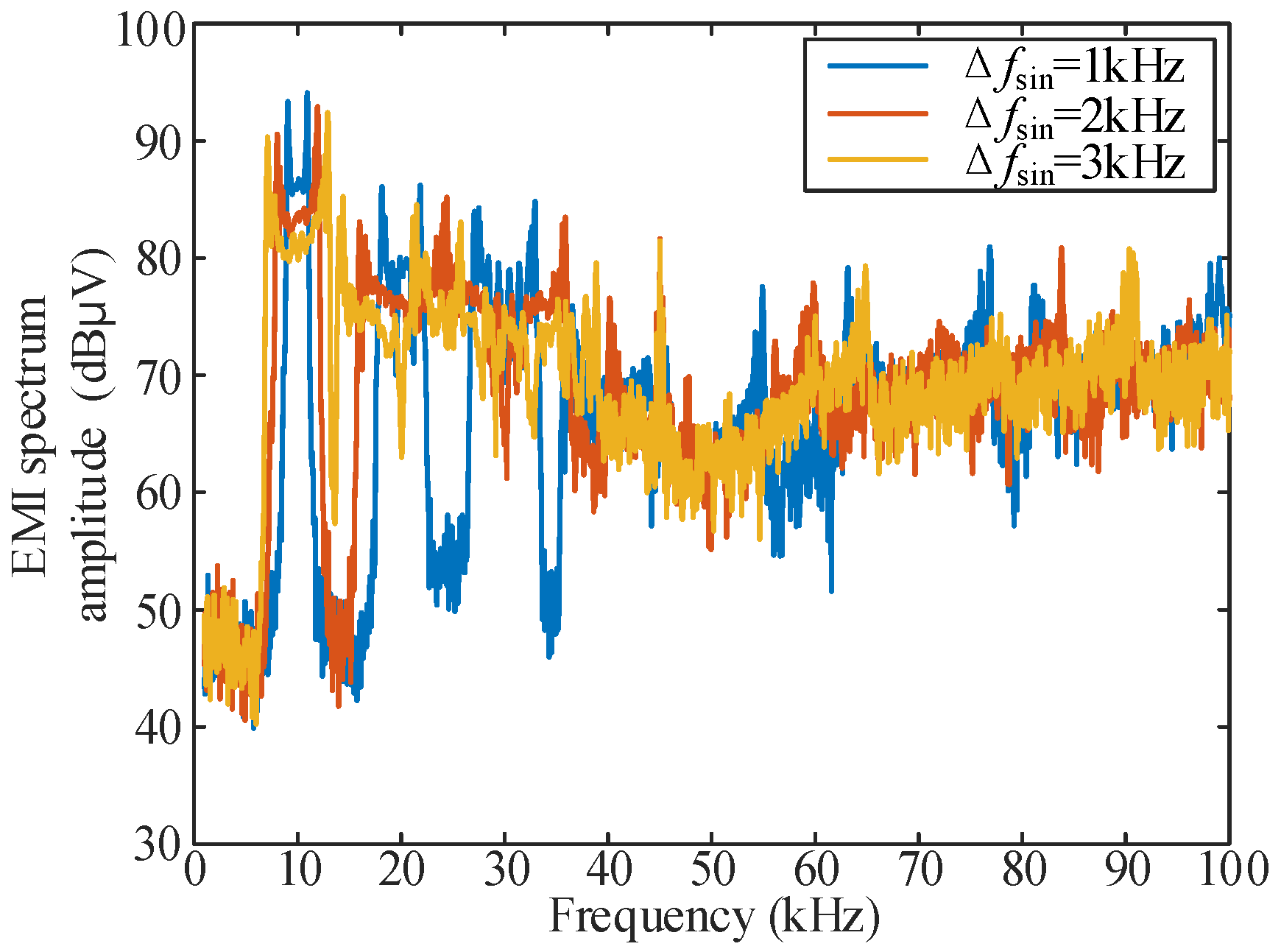
h = 1, 2, 3…. As shown in
Figure 3, the main factor affecting the diffusion degree of the EMI spectrum is Δ
f; the larger Δ
f is, the wider the diffusion degree of EMI spectrum is, and the more it can weaken the EMI spectrum peak to a greater extent. However, only increasing Δ
f to reduce the EMI peak may lead to the phenomenon of “spectrum overlap” [
20]; that is, the originally disjoint frequency bands overlap after the spread spectrum, making the EMI energy of some frequency bands rise, as shown in
Figure 3b,c.
② For periodic signal
vm(
t), the distribution of carrier frequency in different frequency bands is affected by the gradient of periodic signal [
21], which affects the spectrum distribution of EMI. Take the sinusoidal signal as an example: as shown in
Figure 4, the absolute value of the gradient of the sinusoidal signal at the value of 0 is the largest, the carrier frequency value is
fs0, and the action time of
fs0 and its nearby frequency bands is the shortest. The gradient of the sinusoidal signal at the extreme value is 0, and the carrier frequency value is
fs0 ± Δ
f;
fs0 ± Δ
f and its nearby frequency band have the longest action time. Therefore, when
vm(
t) is the sinusoidal signal, the frequency distribution of the carrier will present a trend of “high on both sides and low in the middle”.
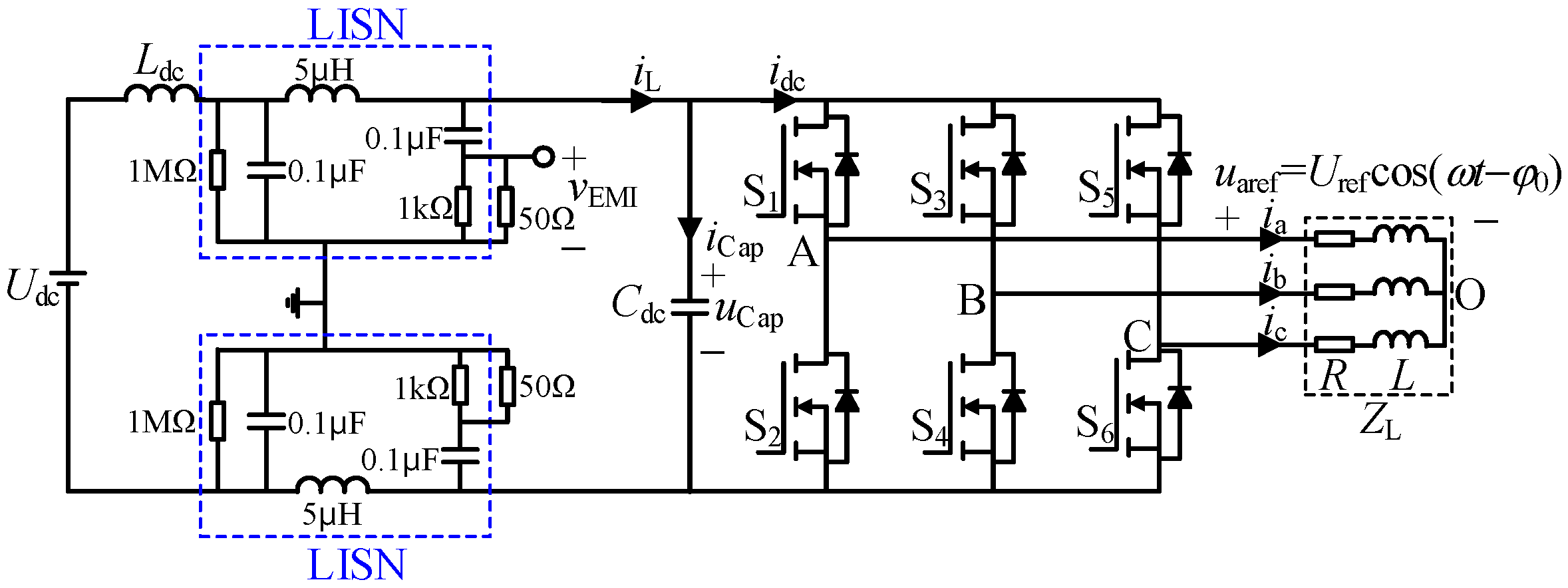
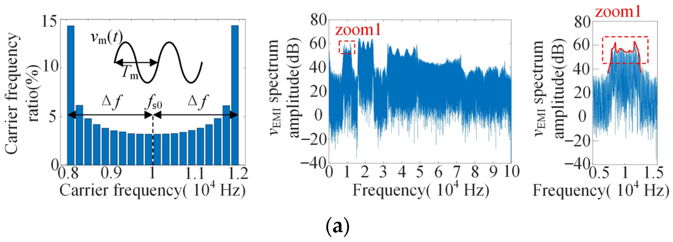
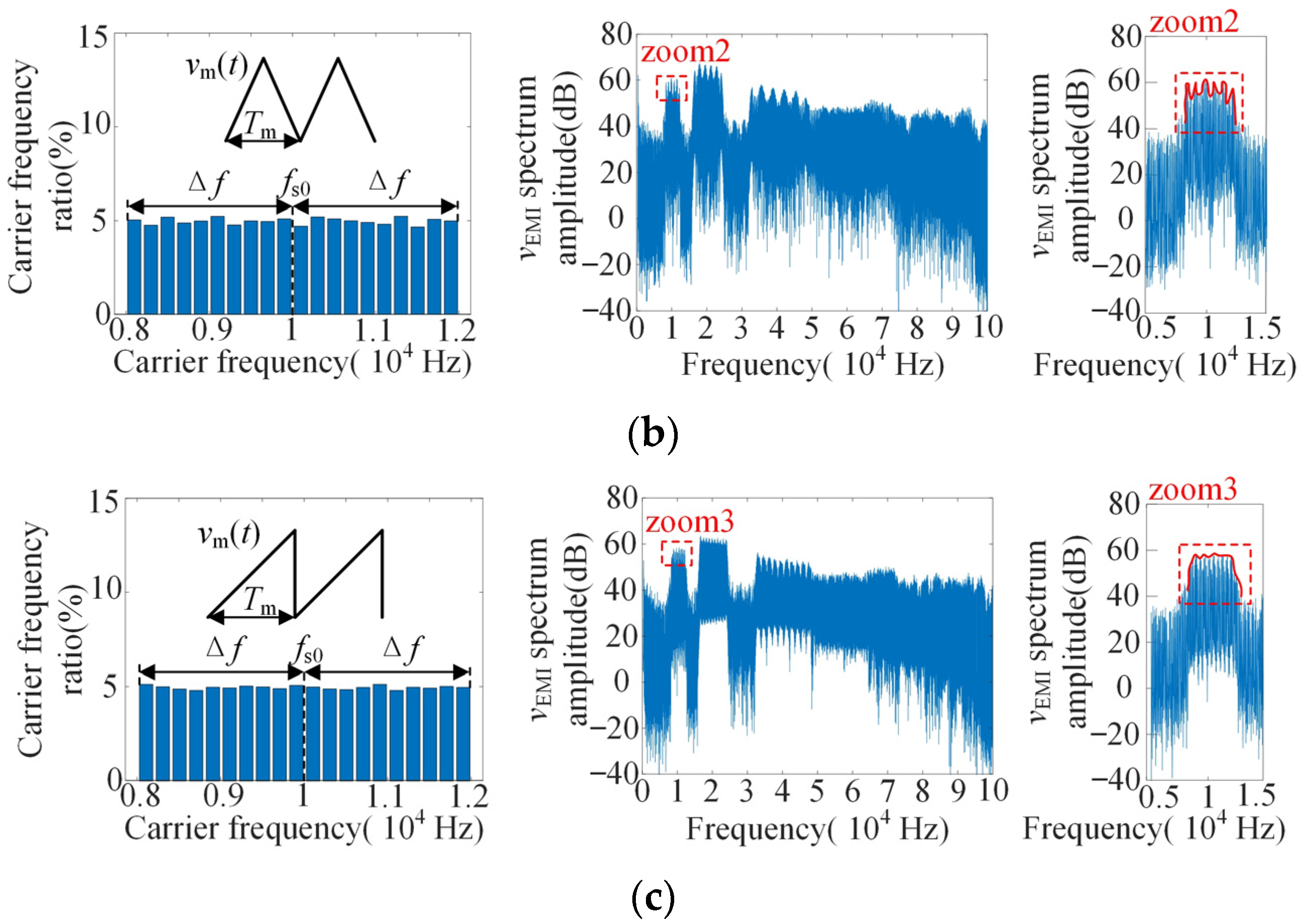
The voltage on the output impedance of LISN (i.e.,
vEMI in
Figure 1) is analyzed by DFT, and its voltage spectrum is used to replace the EMI spectrum to analyze the influence of carrier frequency characteristics on EMI. At Δ
f = 2 kHz,
m = 0.9,
fs0 = 10 kHz,
f1 = 50 Hz,
fm = 30 Hz. When
vm(
t) are sine, triangle and sawtooth, the simulation results are shown in
Figure 5. The figure shows the carrier frequency ratio and the corresponding EMI spectrum distribution.
As shown in the
Figure 5, the distribution characteristics of
vEMI spectrum at the frequency band [
fs0 − Δ
f,
fs0 + Δ
f] is similar to that of the carrier frequency ratio.
3.2. Equivalent Analysis of Voltage and Current Ripple Under Spread Spectrum Modulation
3.2.1. DC Side Voltage Ripple
According to Equation (2), the fluctuation of DC voltage at the input side will, on the one hand, affect the stability of output voltage. On the other hand, the higher voltage ripple has higher requirements for the design of DC support capacitor
Cdc [
17], which will increase the volume and weight of the controller. Therefore, it is necessary to establish a quantitative model for the influence of the spread spectrum modulation strategy on input voltage ripple.
According to the current relationship in the inverter topology in
Figure 1, the capacitor current
iCap, the inductor current
iL and the DC input side current
idc satisfy
iCap =
iL −
idc. The current is decomposed into the sum form of the average value and the fluctuation value:
where
ICap,
IL and
Idc represent the average current value of capacitor
Cdc, the stray inductor
Ldc, and
idc, respectively.
iCap_rip,
iL_rip and
idc_rip represent the corresponding current ripple components. Among them, the relationship of current ripple components satisfies
iCap_rip =
iL_rip −
idc_rip. When the DC filter capacitor is large enough, almost all the ripple components of the input current of the inverter flow through the capacitor, and the ripple current
iL_rip is negligible compared with the ripple current
idc_rip [
17], obtaining:
where
uCap_r is the input voltage ripple.
It can be seen from Equation (11) that the ripple is the integral of the fluctuation quantity with respect to time. Under the spread spectrum modulation, the change of carrier period will affect the input and output waveform ripple.
According to Equations (3) and (4),
idc is determined by
ia,
ib and
ic, and is a cosine function with amplitude
Io, denoted
idc as
Io·cos[
α(
t)], and
α(
t) is the phase of the cosine function with time, which is determined by
ia,
ib and
ic. Ideally,
Io satisfies
, where
R and
L are the resistance and inductance in the load impedance
ZL, respectively; therefore, Equation (11) can be expanded as:
The average value of
idc is expressed as:
So that the voltage ripple expression can be obtained.
According to Equation (11), the DC voltage ripple at the input side can be calculated theoretically, and the quantitative relationship between voltage ripple and each modulation parameter can be established. According to Equation (12), the factors affecting voltage ripple are the integration time Ts and the amplitude of the integration current. Here, Ts = 1/fs(t) = 1/[fs0 + Δf·vm(t)], and the amplitude of the integrated current is related to m and f1. Therefore, according to the above derivation process, the modulation parameters affecting voltage ripple are fs0, Δf, vm(t) (including fm), m and f1, respectively.
3.2.2. AC Side Output Current Ripple
In this section, in order to achieve fast and accurate evaluation of inverter output waveform quality under different modulation methods, the effective value model of motor stator flux fluctuation under the spread spectrum modulation strategy is constructed, which is equivalent to the sum of three-phase output current fluctuation, and can be used to analyze and compare the influence of different periodic signals and spread spectrum modulation parameters on inverter output waveform quality. The steps are as follows: in the vector synthesis process, there is an error voltage vector between the basic vector and the reference vector at any time [
18,
19], and the reference voltage vector is defined as
Uref. Without loss of generality, when the reference vector
Uref is located in sector I, the corresponding error voltage vectors are
U4_err and
U6_err. When the basic voltage vectors
U4 and
U6 act is shown in
Figure 6.
The expressions of the error voltage vectors
U4_err,
U6_err and
U0_err are:
The direction of the reference vector
Uref is defined as the d-axis, and the direction of the leading d-axis π/2 is defined as the q-axis. The error voltage vectors
U4_err,
U6_err and
U0_err are decomposed into the d-axis and the q-axis:
Define
ud0~
ud2 and
uq1~
uq2 as:
According to the motor voltage equation, the integral of the error voltage vector with respect to time within the carrier period
Ts is the stator flux fluctuation
ψrip, as shown in the following equation:
Among them, ud and uq are error voltage components of d-axis and q-axis in different time periods, and their values in different time periods can be represented by ud0~ud2 and uq1~uq2 respectively, as shown in Equation (16).
Furthermore, the effective value
ψrip_rms of the flux fluctuation quantity in time
T can be calculated as:
Among them, to ensure that fs(t) and i(t) contained in the selected time period are all integer periods, T should take at minimum the least common multiple of 1/fm and 1/f1.
According to Equations (16) and (17), the amplitude of flux fluctuation is affected by modulation parameters similar to input voltage ripple, which is mainly determined by the integration time Ts (Ts = 1/[fs0 + Δf·vm(t)]) and the amplitude of the integral component. According to Equation (16), the integral components ud and uq are mainly determined by the amplitude |Uref|, since the modulation parameters affecting ψrip_rms are fs0, Δf, vm(t) (including fm) and m, respectively.
3.2.3. Analysis of the Influence of Spread Spectrum Modulation Parameters on Ripple
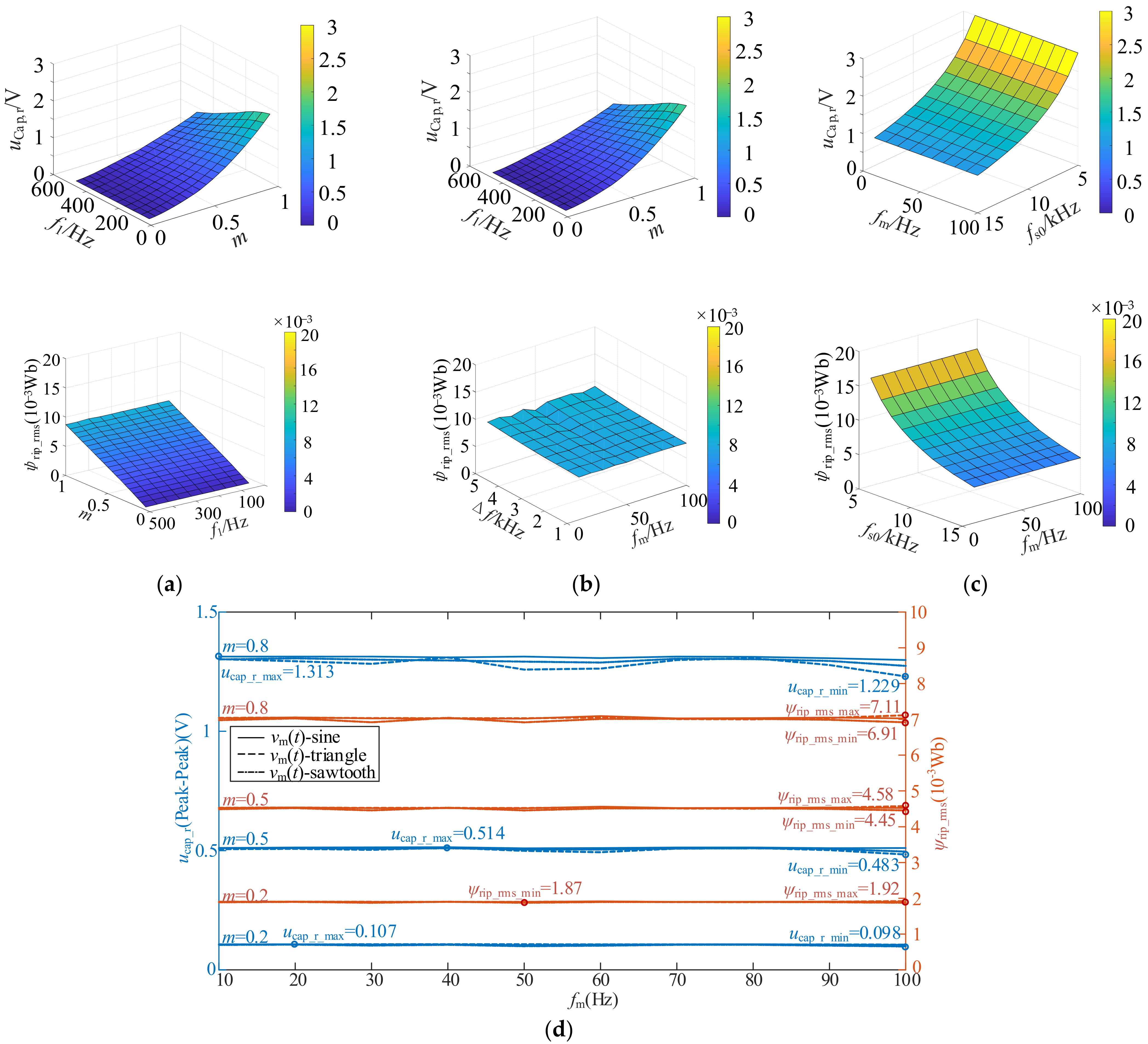
In this section, under the conditions of Udc = 600 V, R = 2.75 Ω, L = 1 mH, Cdc = 1680 μF, the input voltage ripple and flux fluctuation are calculated according to the derived expressions.
The initial values of the five modulation parameters affecting the two indicators are set as follows: fs0 = 10 kHz, Δf = 0 kHz, f1 = 50 Hz, m = 0.9 and fm = 30 Hz, and any two of the five parameters are changed to present the calculation results in the form of a 3D surface graph.
When
vm(
t) is the sawtooth signal, the calculation results are shown in
Figure 7. The results are highly similar when
vm(
t) is sinusoidal signal or triangular signal. Among them,
m = 0.05:0.05:1 means that the modulation index
m starts from 0.05 and changes in the amplitude of 0.05 each time until
m = 1, and the other parameters are expressed in the same way. The integration time
T for calculating the effective value of flux fluctuation quantity in Equation (18) is 1 s. According to the results shown in
Figure 7a–c, the voltage ripple and flux fluctuation are mainly affected by the four parameters of
m,
f1, Δ
f and
fs0, and are not significantly affected by
fm. According to the above results, the variation rules of input voltage ripple and flux fluctuation with each parameter are shown in
Table 1.
In practical applications, the carrier center frequency fs0 is usually fixed, and the modulation index m and fundamental frequency f1 usually change with the change of load conditions. Therefore, the only degrees of freedom that can be changed are Δf and the type of periodic signal vm(t) (including fm).
The influence of the types of periodic signals
vm(
t) and
fm on the input voltage ripple and flux fluctuation is further quantitatively analyzed according to the above derived formula, under the three modulation indexes of
m of 0.2 (low modulation index), 0.5 (medium modulation index) and 0.8 (high modulation index), the voltage ripple and flux fluctuation of three periodic signals of sine, triangle and sawtooth under 10 sets of parameters of
fm = 10:10:100 Hz; that is, 30 sets of calculation results correspond to each modulation condition. Two sets of results and corresponding conditions for the minimum and maximum values of input voltage ripple and flux fluctuation were compared from the 30 sets of results. The other calculated conditions were
fs0 = 10 kHz, Δ
f = 1 kHz and
f1 = 50 Hz, and the specific results are shown in
Figure 7d.
Therefore, by comparing the results in
Figure 7, it can be seen that when the four parameters
m,
fs0, Δ
f and
f1 are all determined,
vm(
t) and
fm have little influence on the input voltage ripple and flux fluctuation. According to
Figure 7d, when the waveform characteristics of
vm(
t) change, the voltage ripple is basically around 1 V, which is very limited compared to the vehicle voltage platform of 800 V. For the flux ripple, which is basically equivalent to the current ripple, its order of magnitude is 10
−3 Wb, which is 1~2 orders of magnitude different from the permanent magnet flux amplitude of the vehicle motor. Therefore, it can be analyzed that in the vehicle scenario, the waveform characteristics of the periodic signal have little influence on the DC side voltage ripple of the inverter, and the influence on the AC side current ripple is relatively limited. When optimizing the modulation strategy, the influence of
vm(
t) waveform characteristics on ripple can be temporarily ignored or less considered.
3.3. Loss Analysis Under Spread Spectrum Modulation
The loss of power switching devices includes switching loss and conduction loss, and switching loss is the main one. Switching loss can be fitted as a quadratic function related to current [
22]:
where,
i(
t) is the current flowing through the switch tube at time
t, and the parameters
A1,
B1 and
C1 can be obtained by curve fitting with double-pulse experimental data. The total loss is usually determined by the single turn-on and turn-off loss of the switch tube and the total switching times per unit time [
22]. In a carrier cycle, the upper and lower switches of the same bridge arm are turned on and off once, so the switching loss can be evaluated equivalently by analyzing the number of carriers included in the corresponding modulation strategy per unit time. The number of carriers included in different modulation strategies within 1 s is shown in
Table 2.
As can be seen from
Table 2, under different Δ
f for different periodic signals, since
fs always fluctuates periodically around
fs0, the number of carriers included in unit time is almost the same, and compared with the fixed carrier frequency condition, the number of carriers is not significantly increased, so it can be considered that the spread spectrum modulation strategy has almost no effect on the switching loss of the inverter. Therefore, based on the above analysis, the influence of modulation strategy on switching loss can be less considered when designing periodic spread spectrum modulation strategy.
3.4. Summary
In summary, for the three parameters of periodic signals, vm(t), fm and Δf, that need to be considered in the design of spread spectrum modulation strategy, it can be concluded that vm(t) and fm have no significant influence on ripple and loss through the mathematical model. Under the premise of weighing multiple indicators, when designing a new spread spectrum modulation strategy, it only needs to focus on limiting Δf to ensure that under the same conditions, compared with the traditional spread spectrum modulation strategy, the conducted EMI is reduced to a greater extent.
4. “Secondary Frequency Modulation” Spread Spectrum Modulation Strategy
According to the above analysis, this paper further proposes a “secondary frequency modulation (secondary FM)” spread spectrum modulation strategy based on sinusoidal signal waveform characteristics, which can reduce the peak value of conducted EMI to a greater extent than single periodic signal spread spectrum modulation within the same frequency fluctuation range, and does not increase additional ripple and loss. The schematic diagram of the spectrum dispersion effect is shown in
Figure 8a. The main idea is explained as follows: on the basis of the spread spectrum modulation of
vm(
t) for sinusoidal signal, the concentrated part of the uneven frequency band of high-frequency and low-frequency is dispersed, so as to further reduce the conducted EMI peak. The spread spectrum modulation of a single sinusoidal signal is denoted as “primary frequency modulation”, and the modulation strategy of dispersing a specific frequency band based on the “primary frequency modulation” is denoted as “secondary FM”. The schematic diagram of carrier frequency change after secondary FM is shown in
Figure 8c, and the design basis of the parameters in the figure is explained as follows:
4.1. Determine the Frequency Band and Diffusion Mode for Secondary Diffusion Based on the Waveform Characteristics of Periodic Signals
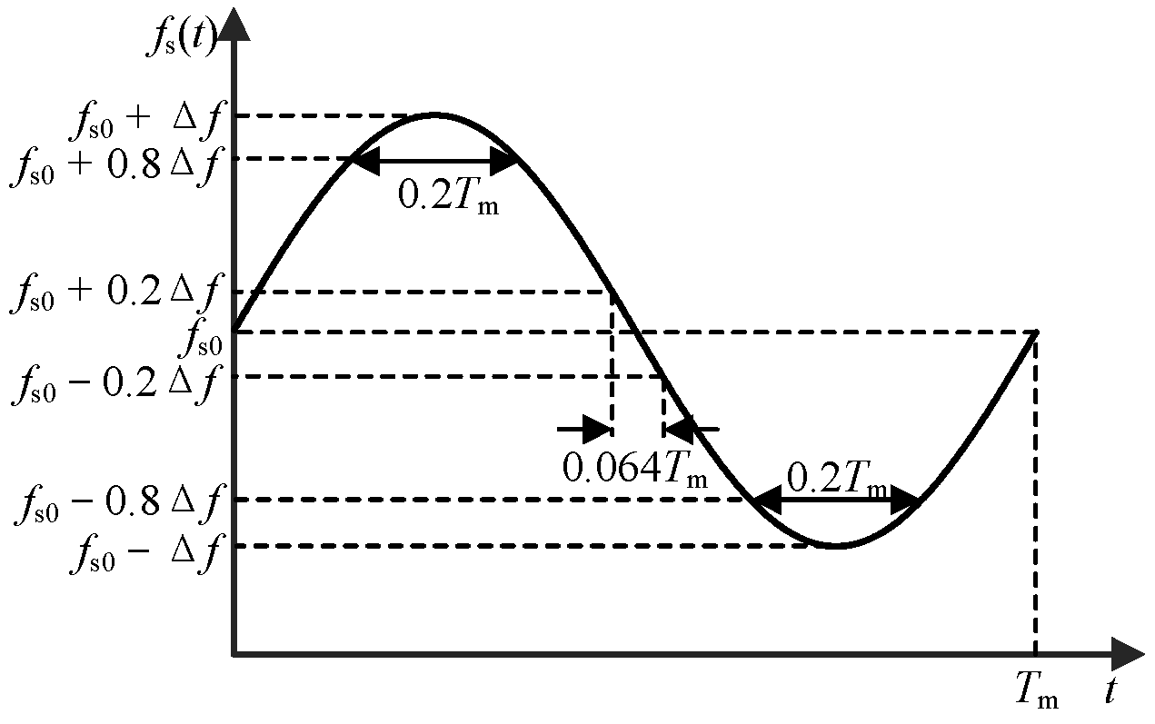
According to
Figure 5a, when
vm(
t) is a sinusoidal signal, part of the frequency bands with uneven carrier frequency distribution are mainly concentrated on both sides of the full frequency band, and the proportion content of the other frequency bands is significantly lower than that of the triangular signal and sawtooth signal. The frequency bands are defined as follows: [
fs0 − Δ
f,
fs0 − 0.8Δ
f] for frequency band ①(FB①), [
fs0 − 0.8Δ
f,
fs0 + 0.8Δ
f] for frequency band ②(FB②), and [
fs0 + 0.8Δ
f,
fs0 + Δ
f] for frequency band ③(FB③). Through the simulation analysis, the EMI peaks of sinusoidal, triangular and sawtooth signals in different frequency bands and adjacent bands are shown in the following table. The parameters of the simulation are:
fs0 = 10 kHz,
m = 0.9,
fm = 30,
f1 = 50 Hz, Δ
f =3 kHz.
As can be seen from
Table 3, when
vm(
t) is a sinusoidal signal, the peak of the
vEMI spectrum is mainly distributed in narrow FB① and FB③, and the EMI spectrum peak in FB② is significantly lower than when
vm(
t) is a triangular signal or a sawtooth signal. Based on this feature, the FB① and FB③ are further spread to further reduce the conducted EMI peak.
In order to distinguish it from the Δ
f of the spread spectrum modulation of a single periodic signal, the frequency deviation variable of the “primary frequency modulation” of the sinusoidal signal in the “secondary FM” strategy is denoted as Δ
fsin. The frequency component in the original FB① is diffused to the frequency band [
fs1,
fs0 − 0.8Δ
fsin], and [
fs1,
fs0 − 0.8Δ
fsin] is denoted as spread spectrum ①(SS①). FB② remains unchanged. The FB③ is spread to [
fs0 + 0.8Δ
fsin,
fs2] band, [
fs0 + 0.8Δ
fsin,
fs2] is denoted as spread spectrum ③(SS③).
fs1 and
fs2 are the lower and upper limits of the fundamental carrier frequency band of “secondary FM”, respectively. According to
Figure 8c, after “secondary FM”, the variation law of the carrier in the two parts of the SS① and SS③ is a piecewise primary function, and
ai and
bi represent the slope and intercept of the carrier frequency expression in different periods, respectively.
4.2. Determine the Value of Δfsin
The selection principle of Δ
fsin is to fully realize the spread spectrum effect of “primary frequency modulation” and reduce the problem of “spectrum overlap” as much as possible. When
vm(
t) is a sinusoidal signal, and the value of Δ
fsin is 1, 2 and 3 kHz, the other parameters of the simulation are set as:
fs0 = 10 kHz,
m = 0.9,
fm = 30,
f1 = 50 Hz. The distribution and characteristic analysis of the EMI peak in the simulation are shown in
Table 4.
Based on the distribution characteristics of the conducted EMI spectrum under different conditions, Δfsin = 2 kHz is finally selected as the basis of the “secondary FM”.
4.3. Determine the Value Range of fs1 and fs2
According to
Figure 5a, FB① and FB③ of the uneven part account for about 20% of the full frequency band, respectively, and the proportion of each component in FB② is less than 5% at most. Therefore, from the perspective of carrier frequency dispersion, the proportion of each component in the dispersed FB① and FB③ (within the length of 0.1Δ
fsin band) should not exceed 5%, so as to ensure that the EMI peak value of the dispersed frequency band is not higher than that of other frequency bands. The width of the frequency band before dispersion is 0.2Δ
fsin, then the width of the frequency band after dispersion should be satisfied:
i.e.,
fs1 ≤
fs0 − 1.2Δ
fsin;
fs2 ≥
fs0 + 1.2Δ
fsinThe lower and upper limits of the fundamental carrier frequency change are defined as
fsmin and
fsmax, respectively. In order to reduce the overlap between “SS① double frequency” and “primary frequency modulation” original frequency band [
fs0 − Δ
fsin,
fs0 + Δ
fsin], as shown in
Figure 9, 2
fs1 ≥
fs0 + Δ
fsin should be satisfied. For
fsmax, it is determined according to |
fsmin −
fs0| = |
fsmax −
fs0|, i.e.,:
Under the condition of Δfsin = 2 kHz, according to Equations (20) and (21), the variation range of fs1 is determined to be [6 kHz,7.6 kHz], and the variation range of fs2 is determined to be [12.4 kHz,14 kHz].
5. Experimental Results and Analysis
In this section, the “secondary FM” strategy and single periodic signal spread spectrum modulation are experimentally studied, and the effect of the traditional spread spectrum modulation strategy and the “secondary FM” on reducing the conducted EMI is analyzed. The input voltage ripple, output current and controller loss under different modulation strategies or different modulation parameters are measured.
The experimental parameters are shown in
Table 5, and the experimental platform is shown in
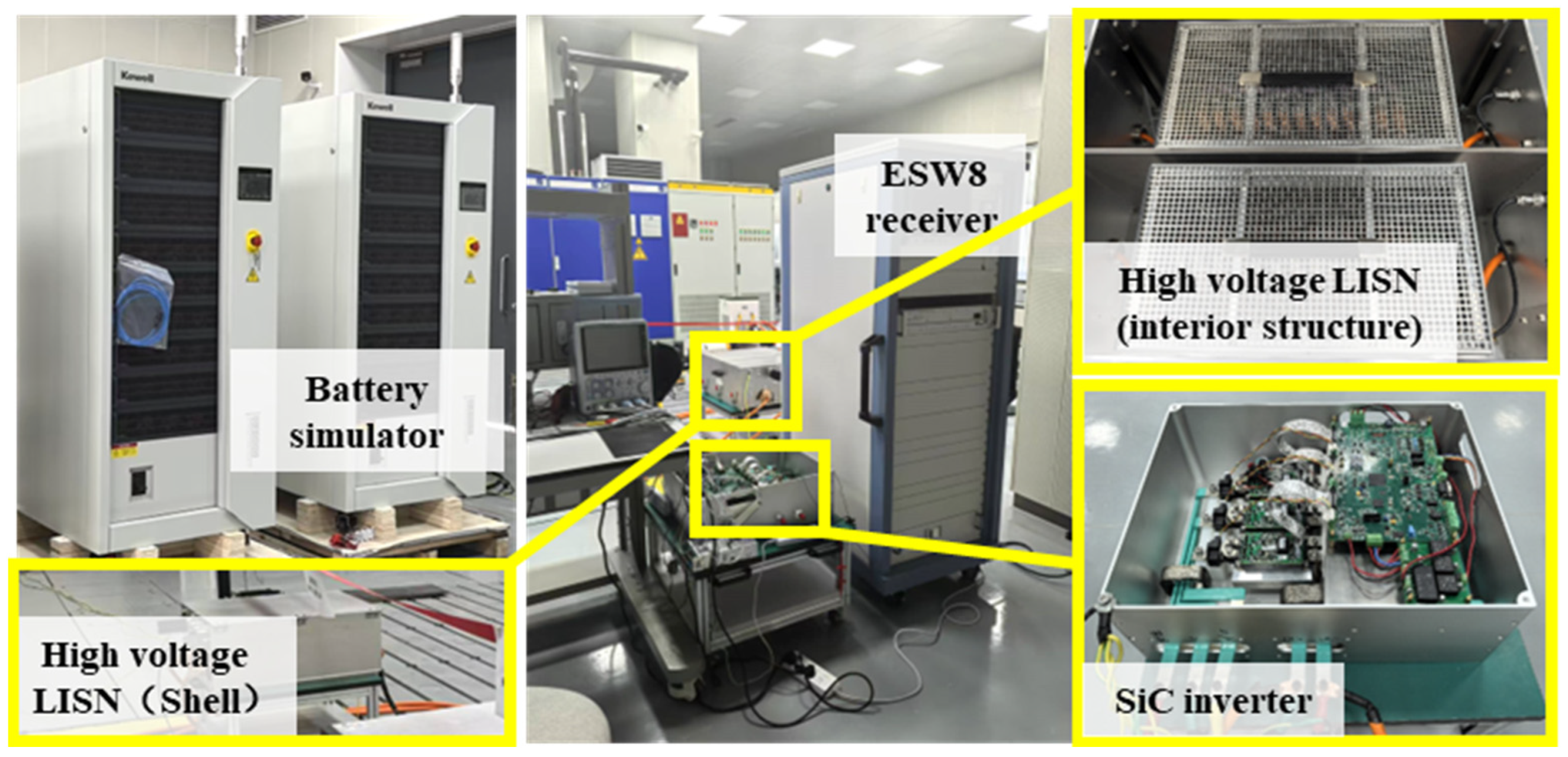
Figure 10. The chip model of the control system is DSP28379, the model of the power semiconductor module is BSM600D12P3G001 SiC module, the DC side is powered by the battery simulator as the DC power supply and connected to the inverter through the NNHV 8123-800 high-voltage LISN of Rhode&Schwartz (Munich, Germany). The LISN load end is connected to the ESW8 receiver for testing the conducted EMI spectrum. The voltage and current ripple are measured by Yokogawa oscilloscope. The loss test is divided into two parts: the double-pulse test for measuring the characteristics of the inverter switch tube, and the loss test for measuring the efficiency of the inverter. The double-pulse test is completed by the Edison DPT2K04B (Dongguan, China) power device dynamic parameter measurement instrument, and the loss test is completed by the Yokogawa (Tokyo, Japan) WT5000 power analyzer.
5.1. Experimental Parameter Design of “Secondary FM” Modulation Strategy
The EMI spectrum distribution characteristics of a single sinusoidal signal with spread spectrum modulation in three cases of Δ
fsin = 1, 2 and 3 kHz are tested experimentally, and the results are shown in
Figure 11.
According to
Figure 11, for Δ
fsin = 1, 2, 3 kHz, the lowest amplitude of the EMI spectrum of the spread spectrum modulation of the sine signal in [
fs0 − Δ
fsin,
fs0 + Δ
fsin] band is shown in
Table 6. The spectrum distribution characteristics under the three conditions in
Figure 11 are highly similar to the analysis in
Table 4, and according to the results shown in
Figure 11 and
Table 6, it can be seen that the selection of Δ
fsin = 2 kHz as the basic condition of “secondary FM” is still reasonable in the actual experiment.
5.2. Comparison of EMI Experimental Results
In this section, the traditional period spread spectrum modulation strategy and the “secondary FM” strategy proposed in this paper are tested, to verify and compare the effects of different strategies on reducing the conducted EMI peak.
5.2.1. EMI Results of Spread Spectrum Modulation of Single Periodic Signal
In order to verify the effect of spread spectrum modulation of a single periodic signal on reducing the conducted EMI spike, the EMI spectrum of fixed carrier frequency modulation and
vm(
t)-sine,
vm(
t)-triangle,
vm(
t)-sawtooth spread spectrum modulation at Δ
f = 1 kHz was tested, and the results are shown in
Figure 12.
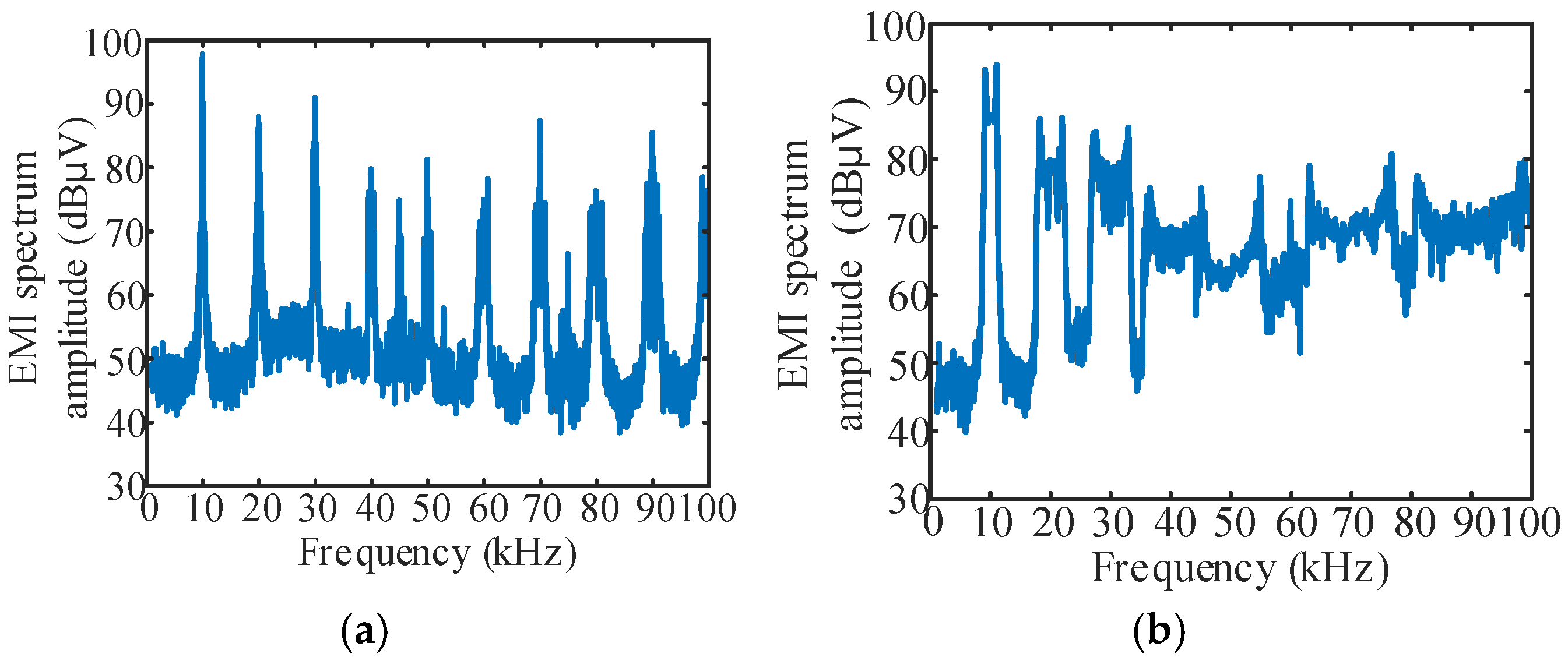
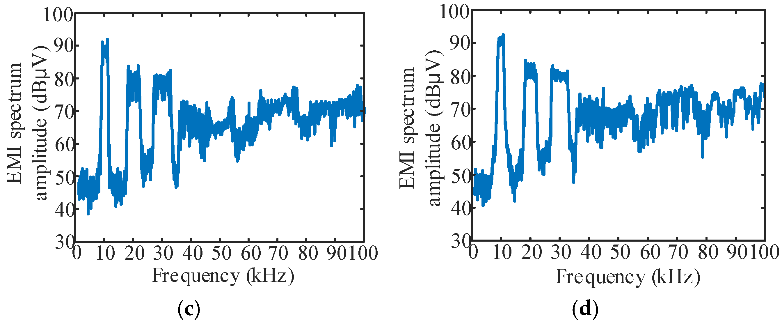
It can be seen from the figure that the peak value of conducted EMI under a fixed carrier frequency of 10 kHz is 98.03 dBμV, and the peak value of conducted EMI corresponding to sine, triangle and sawtooth signals under Δf = 1 kHz is 94.11 dBμV, 92.1 dBμV and 92.52 dBμV, respectively, which are lower than those under a fixed carrier frequency modulation.
In order to analyze the influence of
vm(
t) and Δ
f on conducted EMI,
vm(
t)-sine,
vm(
t)-triangle,
vm(
t)-sawtooth spread spectrum modulation were tested, respectively, and the conducted EMI peak values corresponding to different conditions of Δ
f = 1 kHz:0.1 kHz:4 kHz (that is, all cases of carrier frequency fluctuation in the range of 6 kHz to 14 kHz) were measured. A total of 93 groups of data were collected. The measurement results are shown in
Figure 13, where the lowest peak value of conducted EMI and the corresponding Δ
f under spread spectrum modulation are also marked.
Figure 13 shows that the EMI peak does not decrease monotonically with the increase of Δ
f, corresponding to the “spectrum overlap” phenomenon analyzed; therefore, the purpose of reducing the conducted EMI peak cannot be achieved by simply increasing Δ
f.
5.2.2. Analysis of EMI Experimental Results of “Secondary FM” Spread Spectrum Modulation Strategy
At Δ
fsin = 2 kHz, the FB① and FB③ were dispersed as described in
Section 4. That is, the frequency band of the sinusoidal signal is [8.4 kHz, 11.6 kHz], the [8 kHz, 8.4 kHz] frequency band is separately dispersed into [
fs1, 8.4 kHz], and the [11.6 kHz, 12 kHz] frequency band is dispersed into the [11.6 kHz,
fs2] frequency band. The results under different combinations of
fs1 and
fs2 parameters were tested, and partial results are shown in
Figure 14.
By comparing the results of
Figure 13 and
Figure 14a, the “secondary FM” strategy can achieve a better EMI peak reduction effect than the single periodic signal spread spectrum modulation in the
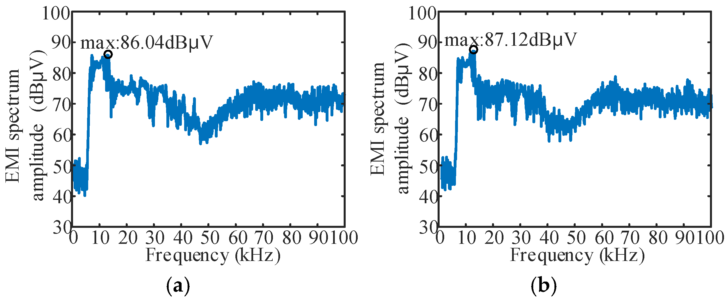
fs range of 6 k~14 kHz. The optimal effect of the “secondary FM” method is reduced by an additional 1.5 dBμV on the basis of 87.54 dBμV in
Figure 13. The comparison of results in
Figure 13 and
Figure 14b shows that with the same or lower Δ
f, “secondary FM” can also achieve better EMI peak reduction effect.
5.3. Input Voltage and Output Current Ripple
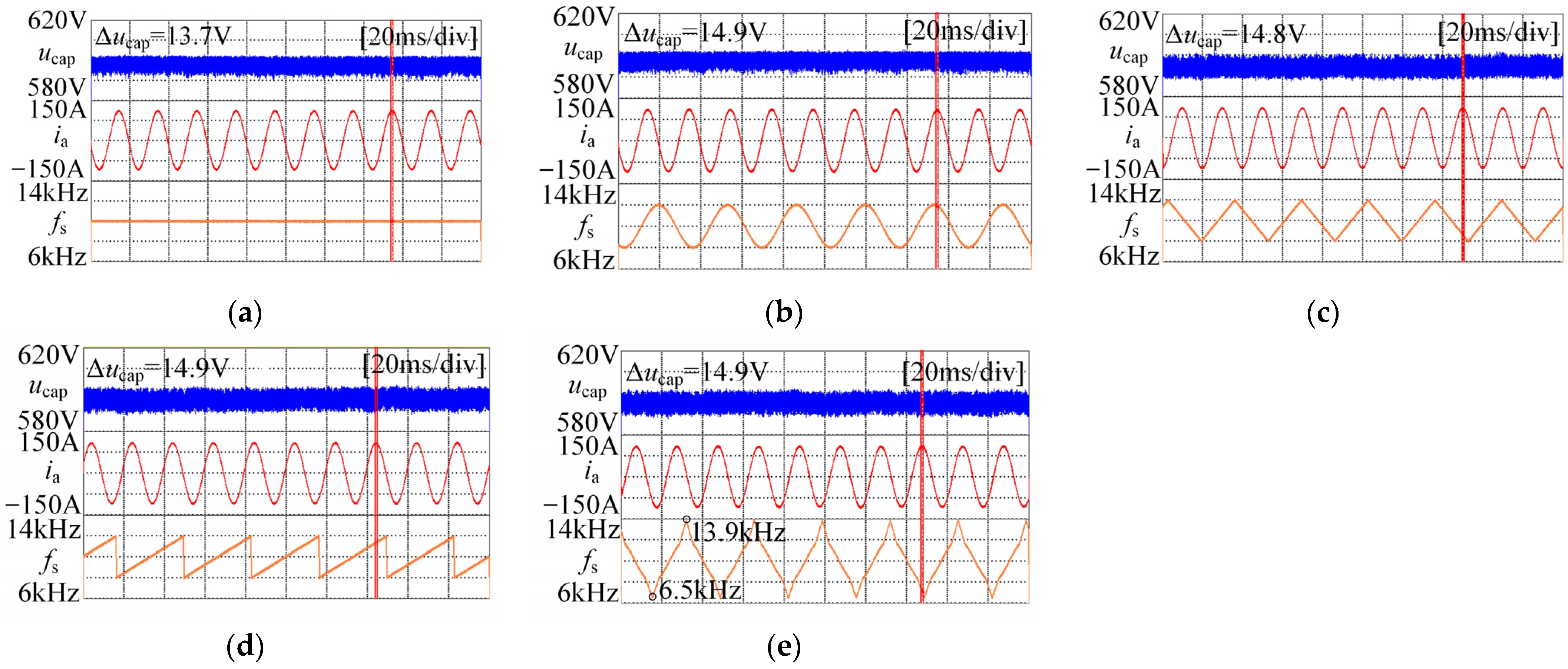
In this section, the input voltage ripple and output current of different modulation strategies are tested, respectively, and the results are shown in
Figure 15. It can be seen from the figure that for input voltage ripple, the maximum difference of voltage ripple under different conditions is only 1.2 V, which is not much different from the input voltage ripple under fixed carrier frequency. Compared with 600 V DC bus voltage, the increase of ripple is only 0.2%.
As for the output current, it can be seen from
Figure 15 that there is no obvious distortion of the output phase current, indicating that the spread spectrum modulation strategy will not significantly affect the quality of the output current.
5.4. Loss Testing
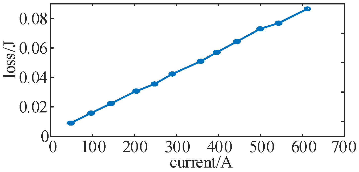
In this section, the double-pulse experiment is carried out to test the switching tube loss data under 12 different switching currents, starting from 50 A and increasing by 50 A until 600 A each time. The relationship between the corresponding current and switching loss is shown in
Figure 16.
According to the results shown in
Figure 16, each parameter in Equation (19) is identified and obtained:
Under the experimental parameters shown in
Table 5, combined with Equations (3) and (22), the expression of switching loss in a single carrier cycle at different times and different currents can be obtained as:
The total switching loss of the inverter per unit time can be obtained by accumulating the switching loss at different times. Taking the Δ
f = 1 kHz condition as an example, the numerical theoretical evaluation of switching loss within 1 s for different modulation strategies is shown in
Table 7.
When
vm(
t) is three kinds of periodic signals, the input and output power, efficiency and loss under different Δ
f are measured by the power analyzer, and the results are shown in
Figure 17. The figure contains the experimental data of three kinds of periodic signals under the condition of Δ
f = 1 kHz:0.1 kHz:4 kHz.
In addition, the loss test results of three typical modulation strategies are selected for presentation, as shown in
Figure 18.
Figure 17 and
Figure 18 show that there is almost no difference between different types of spread spectrum modulation strategies and fixed carrier frequency modulation in terms of loss and efficiency. In addition, the loss results tested by the power analyzer are very close to the loss evaluation results fitted based on the two-pulse experiment in
Table 7, which verifies the effectiveness of the method of indirectly evaluating switching loss through the number of carriers included in the unit time in the spread spectrum modulation strategy. Therefore, in general, when designing the spread spectrum modulation strategy, its impact on the loss can be ignored under the premise that the average carrier frequency does not change much.
6. Conclusions
In this paper, the factors affecting the conducted EMI of the motor controller are analyzed, and the impact level of the spread spectrum modulation strategy on the input DC voltage ripple, output AC current ripple, and controller loss is theoretically evaluated. On this basis, a “secondary FM” spread spectrum modulation strategy is further proposed. Research shows that:
(1) In the single periodic signal spread spectrum modulation, the sawtooth signal has the best suppression effect on EMI peak;
(2) When fs0 is fixed, the influence of spread spectrum modulation on input voltage ripple and stator flux fluctuation mainly depends on Δf. The larger Δf is, the larger input voltage ripple and stator flux fluctuation are, while the type of periodic signal and fm have little effect on them.
(3) The influence of spread spectrum modulation strategy on controller loss is negligible.
(4) In the limited range of carrier frequency variation, compared with the traditional period spread spectrum modulation strategy, the “secondary FM” strategy can further reduce the conducted EMI of the motor controller, the reduced amplitude of conducted EMI is 1.5 dBμV, and this method does not have significant impact on the ripple, loss and other indicators.
Compared with the existing research, the influence of spread spectrum modulation strategy on the input/output performance and loss of the inverter is theoretically analyzed in this paper. The existing research on these indicators under the spread spectrum modulation strategy is usually directly through the experiment, which lacks theoretical analysis. This paper theoretically makes up for this deficiency.


