
A Low-Voltage Low-Power Voltage-to-Current Converter with Low Temperature Coefficient Design Awareness


Abstract
1. Introduction
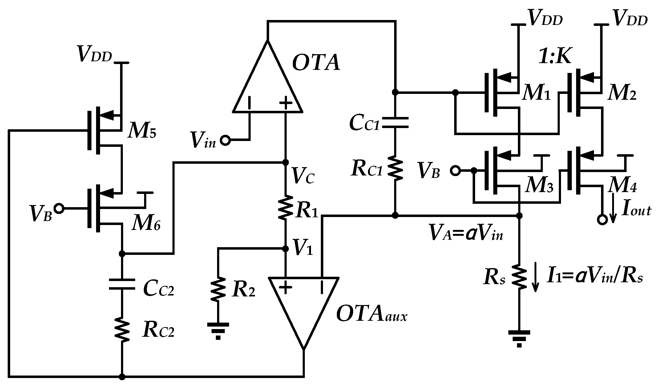
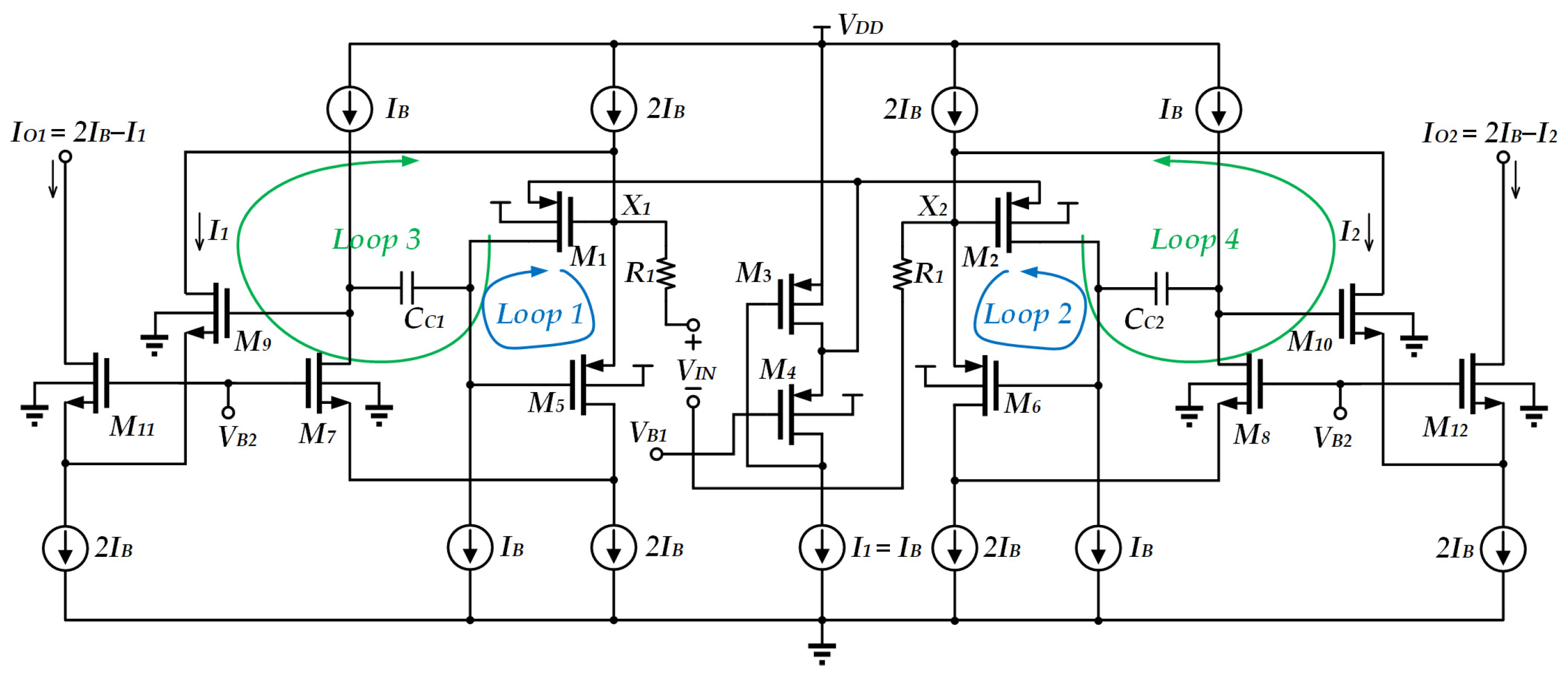
2. Review of V-I Converters
3. Proposed V-I Converter
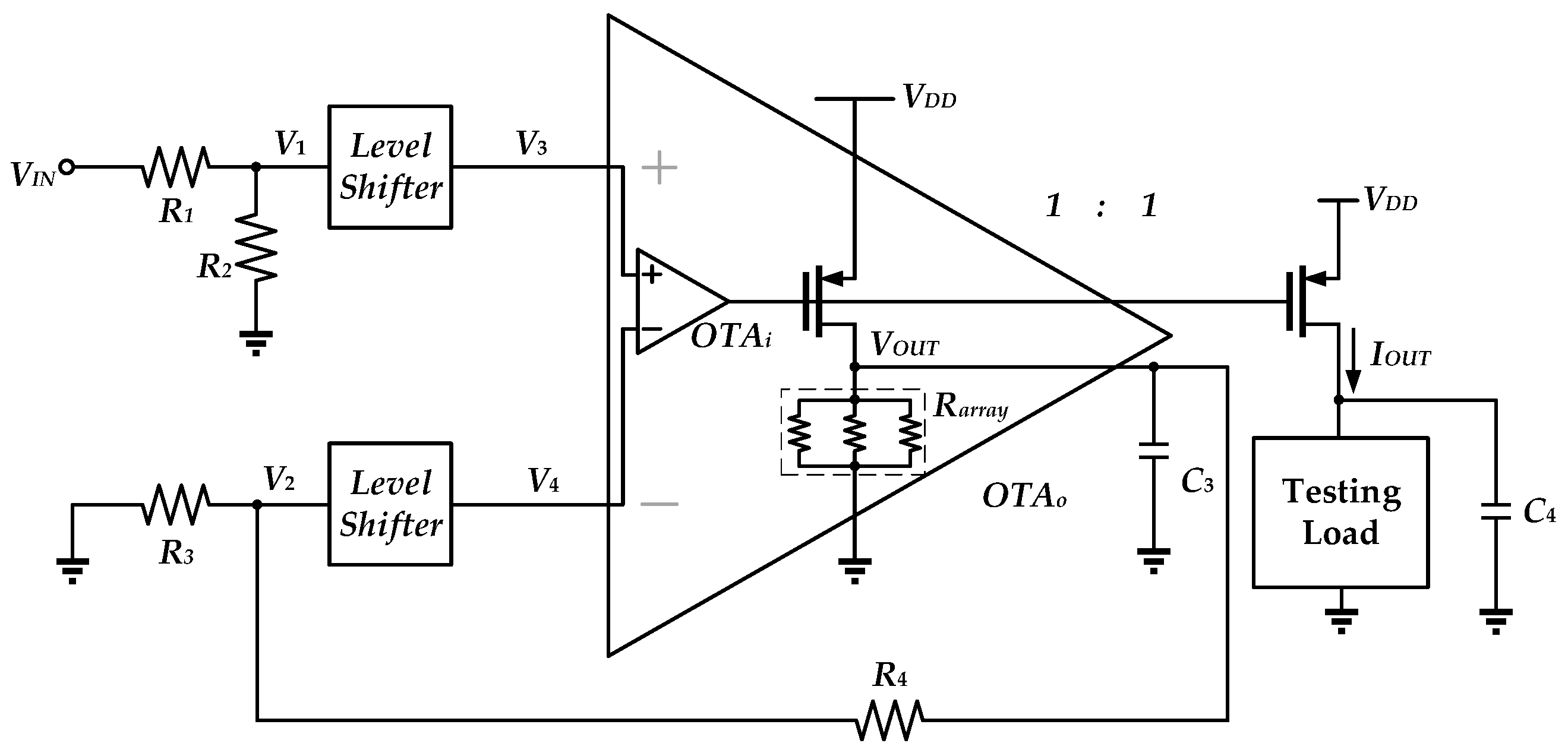
3.1. V-I Converter Architecture
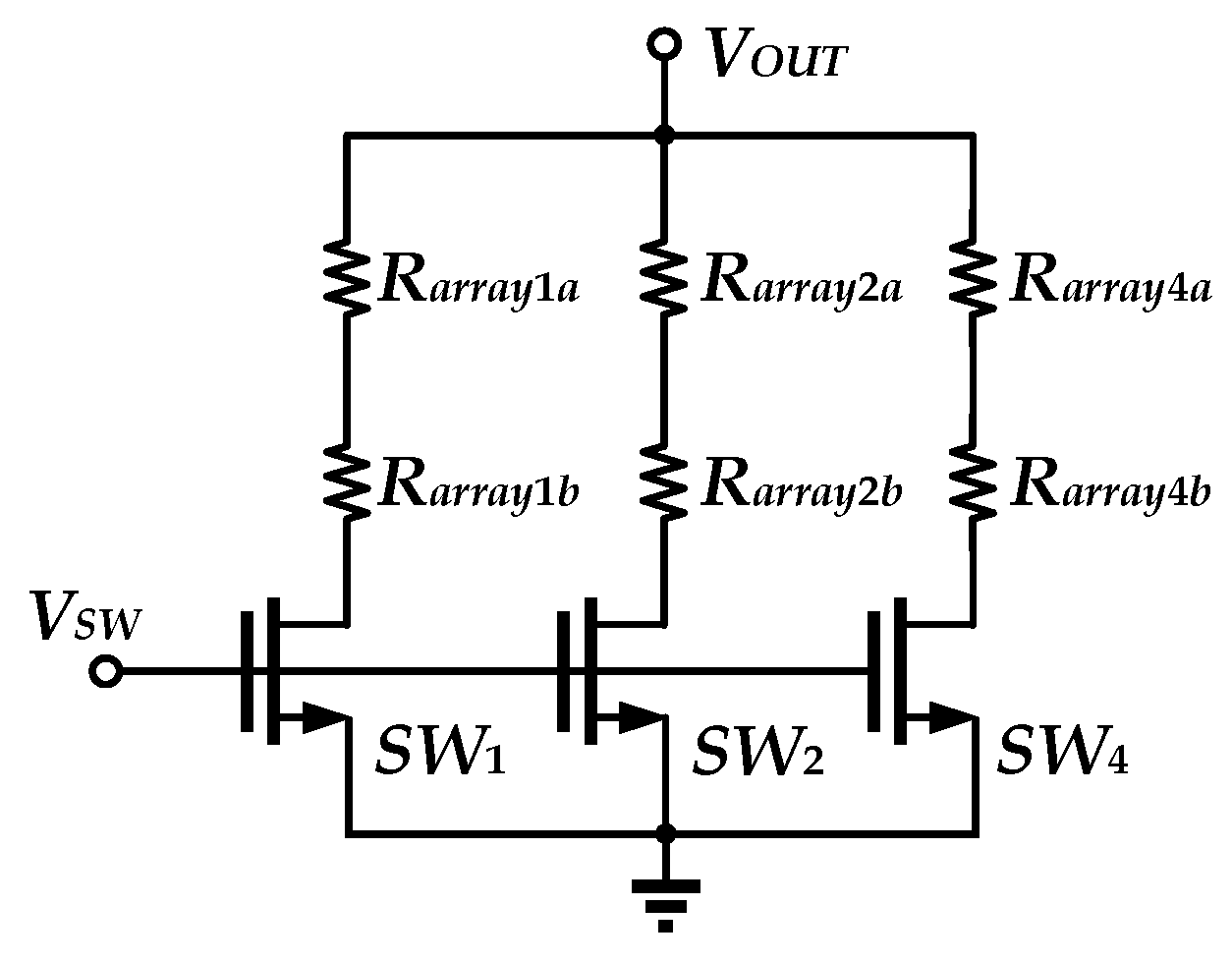
3.1.1. Design of Pseudo Resistor (PR)
3.1.2. Design of Level Shifter
3.1.3. Design of OTAo
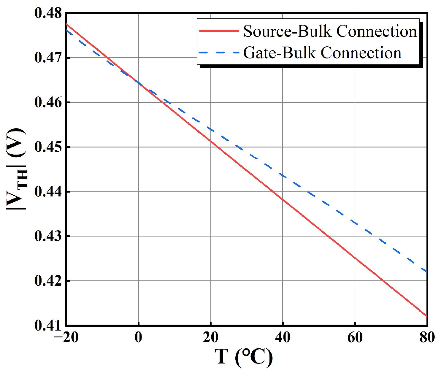
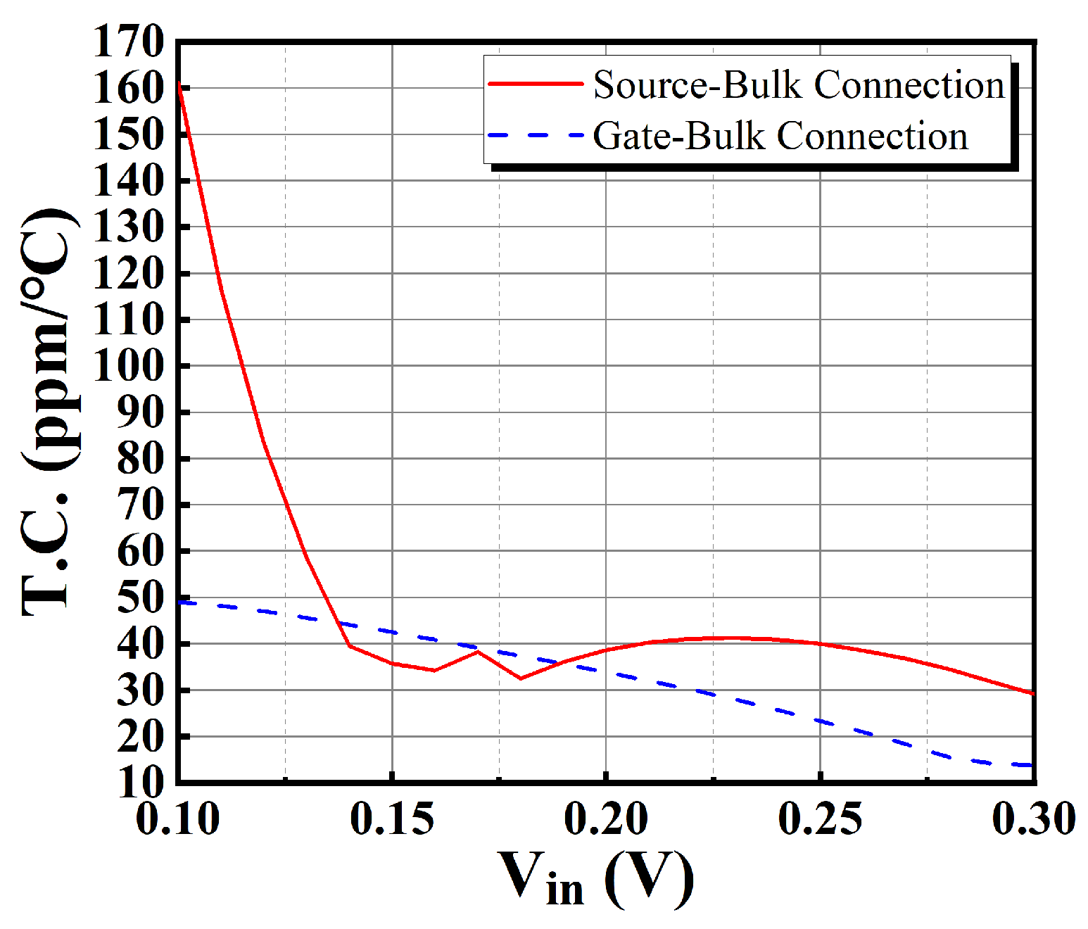
3.2. Temperature Compensation of Proposed V-I Converter
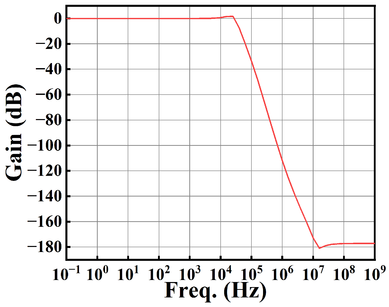
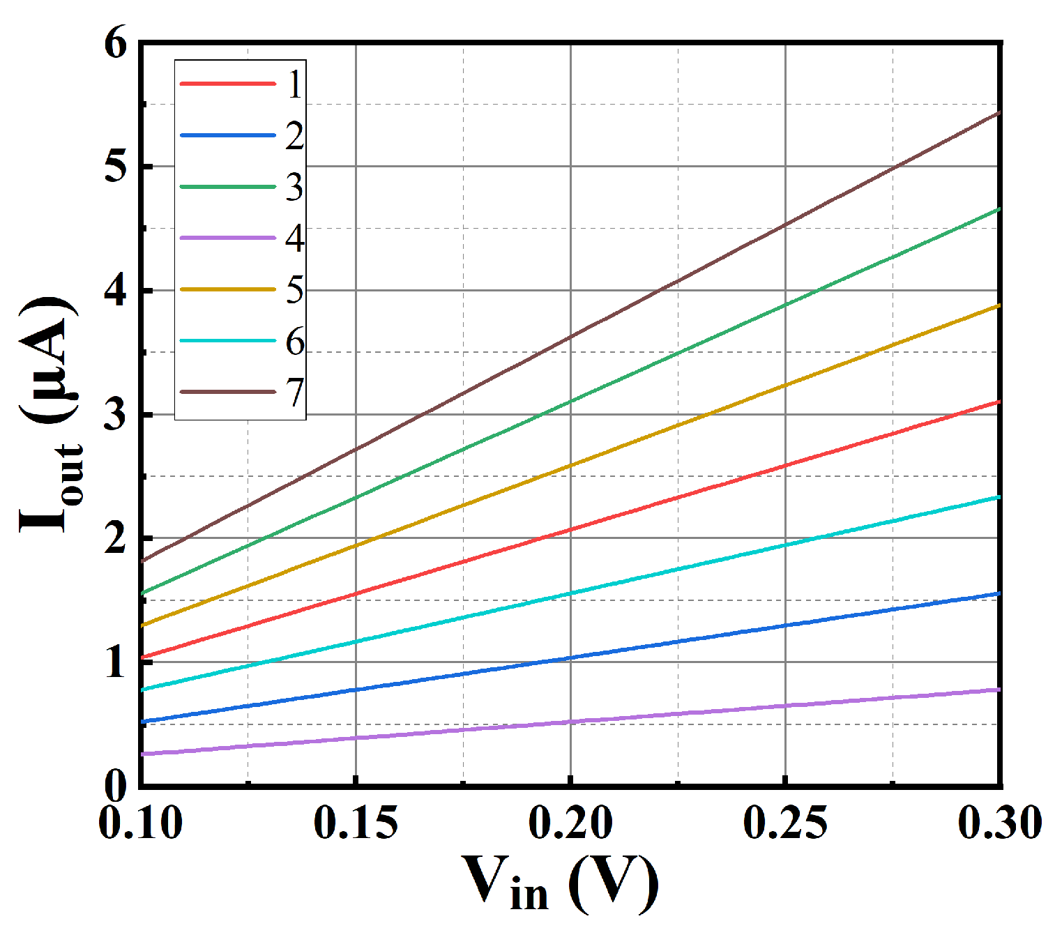
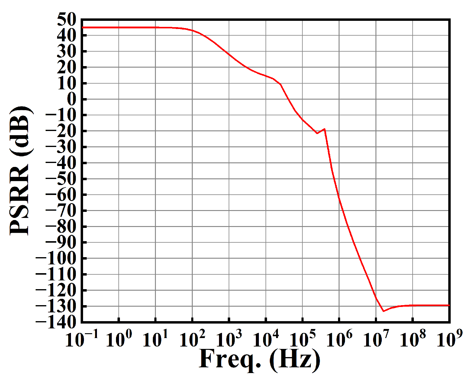
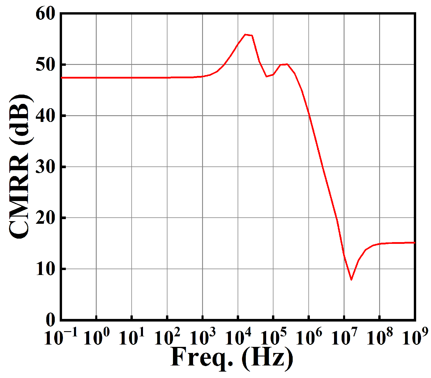
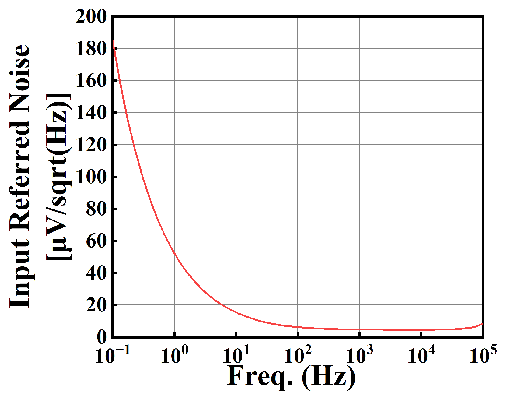
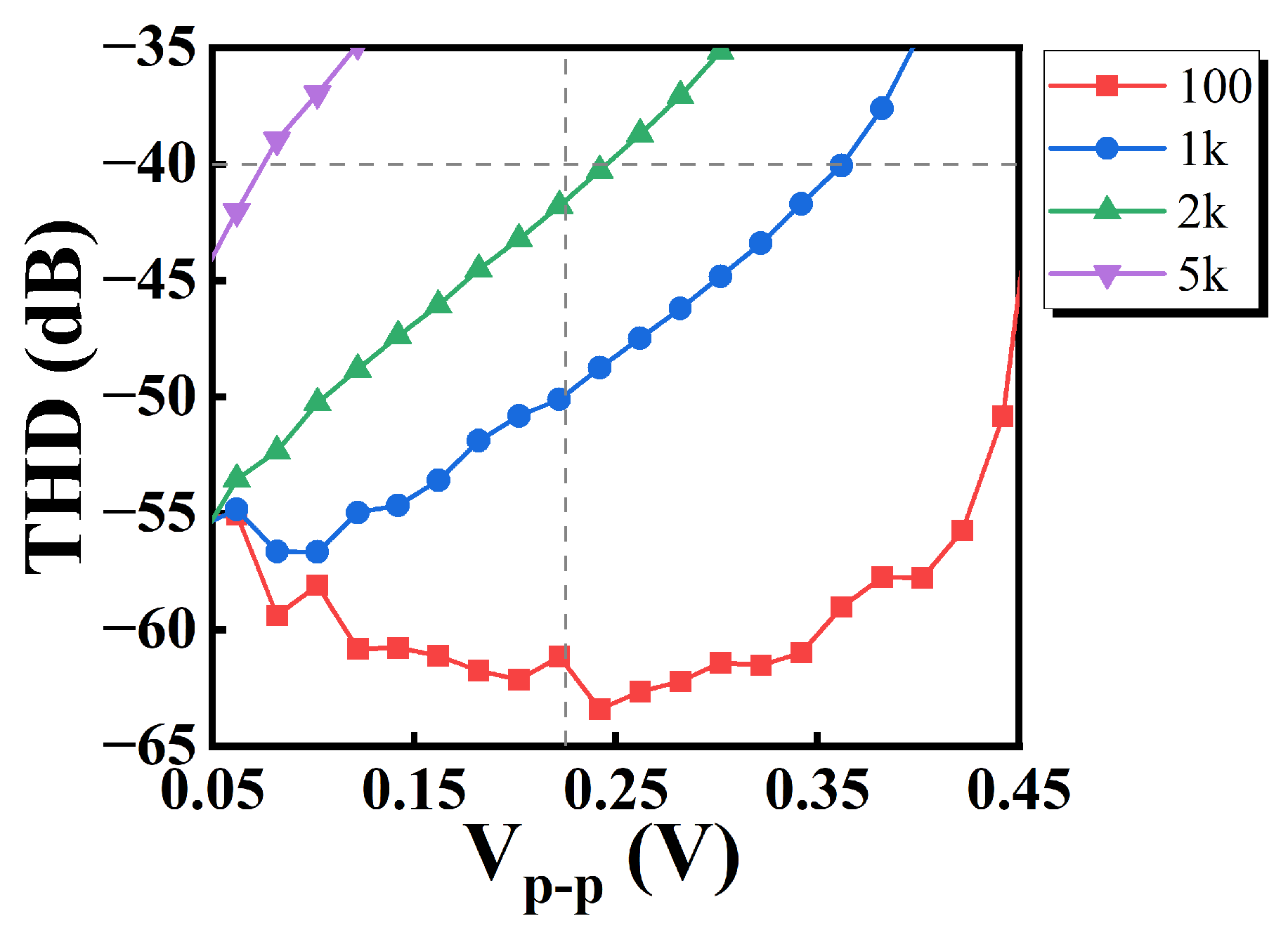
4. Results and Discussions
5. Conclusions
Author Contributions
Funding
Institutional Review Board Statement
Informed Consent Statement
Data Availability Statement
Conflicts of Interest
References
- Rakus, M.; Stopjakova, V.; Arbet, D. Comparison of gate-driven and bulk-driven current mirror topologies. In Proceedings of the 2016 IEEE 19th International Symposium on Design and Diagnostics of Electronic Circuits & Systems (DDECS), Košice, Slovakia, 20–22 April 2016; pp. 1–4. [Google Scholar] [CrossRef]
- Grasso, A.D.; Marano, D.; Palumbo, G.; Pennisi, S. Design Methodology of Subthreshold Three-Stage CMOS OTAs Suitable for Ultra-Low-Power Low-Area and High Driving Capability. IEEE Trans. Circuits Syst. I Regul. Pap. 2015, 62, 1453–1462. [Google Scholar] [CrossRef]
- Ferreira, L.H.C.; Sonkusale, S.R. A 60-dB Gain OTA Operating at 0.25-V Power Supply in 130-nm Digital CMOS Process. IEEE Trans. Circuits Syst. I Regul. Pap. 2014, 61, 1609–1617. [Google Scholar] [CrossRef]
- Lo, T.-Y.; Hung, C.-C. 1-V Linear CMOS Transconductor with -65dB THD innAno-Scale CMOS Technology. In Proceedings of the 2007 IEEE International Symposium on Circuits and Systems (ISCAS), New Orleans, LA, USA, 27–20 May 2007; pp. 3792–3795. [Google Scholar] [CrossRef]
- Colletta, G.D.; Ferreira, L.H.; Pimenta, T.C. A 0.25-V 22-nS symmetrical bulk-driven OTA for low-frequency Gm -C applications in 130-nm digital CMOS process. Analog Integr. Circuits Signal Process. 2014, 81, 377–383. [Google Scholar] [CrossRef]
- Yang, G.-Z. Implantable Sensors and Systems: From Theory to Practice; Springer: Cham, Switzerland, 2018; pp. 387–390. [Google Scholar] [CrossRef]
- Azcona, C.; Calvo, B.; Celma, S.; Medrano, N.; Martinez, P.A. Low-Voltage Low-Power CMOS Rail-to-Rail Voltage-to-Current Converters. IEEE Trans. Circuits Syst. I Regul. Pap. 2013, 60, 2333–2342. [Google Scholar] [CrossRef]
- Jakusz, J.; Jendernalik, W.; Blakiewicz, G.; Kłosowski, M.; Szczepański, S. A 1-nS 1-V Sub-1-µW Linear CMOS OTA with Rail-to-Rail Input for Hz-Band Sensory Interfaces. Sensors 2020, 20, 3303. [Google Scholar] [CrossRef]
- Silva-Martinez, J.; Salcedo-Suner, J. A CMOS automatic gain control for hearing aid devices. In Proceedings of the 1998 IEEE International Symposium on Circuits and Systems (ISCAS), Monterey, CA, USA, 31 May–3 June 1998; Volume 1, pp. 297–300. [Google Scholar] [CrossRef]
- Li, F.; Yang, H.; Liu, F.; Yin, T.; Wang, X. Dual-mode gain control for a 1 V CMOS hearing aid device with enhanced accuracy and energy-efficiency. Analog Integr. Circuits Signal Process. 2012, 72, 495–504. [Google Scholar] [CrossRef]
- Wang, Y.; Cao, R.; Li, C.; Dean, R.N. Concepts, Roadmaps and Challenges of Ovenized MEMS Gyroscopes: A Review. IEEE Sens. J. 2021, 21, 92–119. [Google Scholar] [CrossRef]
- Singhal, N.; Sharma, R.K. Design of 4.9 GHz Current starved VCO for PLL and CDR. In Proceedings of the 2018 5th International Conference on Signal Processing and Integrated Networks (SPIN), Noida, India, 22–23 February 2018; pp. 864–867. [Google Scholar] [CrossRef]
- Wang, C.-C.; Lee, T.-J.; Li, C.-C.; Hu, R. An All-MOS High-Linearity Voltage-to-Frequency Converter Chip with 520-kHz/V Sensitivity. IEEE Trans. Circuits Syst. 2 Analog Digit. Signal Process. 2006, 53, 744–747. [Google Scholar] [CrossRef]
- López-Martín, A.J.; Ramirez-Angulo, J.; Carvajal, R.G. 1.5 V 3 mW CMOS V–I converter with 75 dB SFDR for 6 V pp input swings. Electron. Lett. 2007, 43, 336–338. [Google Scholar] [CrossRef]
- Khateb, F.; Kulej, T.; Vlassis, S. Extremely Low-Voltage Bulk-Driven Tunable Transconductor. Circuits Syst. Signal Process. 2017, 36, 511–524. [Google Scholar] [CrossRef]
- Ghosh, S.; Bhadauria, V. An ultra-low-power near rail-to-rail pseudo-differential subthreshold gate-driven OTA with improved small and large signal performances. Analog Integr. Circuits Signal Process. 2021, 109, 345–366. [Google Scholar] [CrossRef]
- Rico-Aniles, H.D.; Ramirez-Angulo, J.; Lopez-Martin, A.J.; Carvajal, R.G. 360 nW Gate-Driven Ultra-Low Voltage CMOS Linear Transconductor With 1 MHz Bandwidth and Wide Input Range. IEEE Trans. Circuits Syst. II Express Briefs 2020, 67, 2332–2336. [Google Scholar] [CrossRef]
- Delbruck; Mead, C.A. Adaptive photoreceptor with wide dynamic range. In Proceedings of the 1994 IEEE International Symposium on Circuits and Systems (ISCAS), London, UK, 30 May–2 June 1994; Volume 4, pp. 339–342. [Google Scholar] [CrossRef]
- Ramirez-Angulo, J.; Carvajal, R.G.; Galan, J.A.; Lopez-Martin, A. A free but efficient low-voltage class-AB two-stage operational amplifier. IEEE Trans. Circuits Syst. II Express Briefs 2006, 53, 568–571. [Google Scholar] [CrossRef]
- Djekic, D.; Fantner, G.; Lips, K.; Ortmanns, M.; Anders, J. A 0.1% THD, 1-M Ω to 1-G Ω Tunable, Temperature-Compensated Transimpedance Amplifier Using a Multi-Element Pseudo-Resistor. IEEE J. Solid-State Circuits 2018, 53, 1913–1923. [Google Scholar] [CrossRef]
- Benko, P.L.; Galeti, M.; Pereira, C.F.; Lucchi, J.C.; Giacomini, R. Innovative approach for electrical characterisation of pseudo-resistors. Electron. Lett. 2016, 52, 2031–2032. [Google Scholar] [CrossRef]
- Wang, S.; Lopez, C.M.; Ballini, M.; Van Helleputte, N. Leakage compensation scheme for ultra-high-resistance pseudo-resistors in neural amplifiers. Electron. Lett. 2018, 54, 270–272. [Google Scholar] [CrossRef]
- Lau, S.K.; Mok, P.K.T.; Leung, K. A Low-Dropout Regulator for SoC With Q-Reduction. IEEE J. Solid-State Circuits 2007, 42, 658–664. [Google Scholar] [CrossRef]
- Leung, K.; Mok, P.K.T. Analysis of multistage amplifier-frequency compensation. IEEE Trans. Circuits Syst. 1 Fundam. Theory Appl. 2001, 48, 1041–1056. [Google Scholar] [CrossRef]
- Zhang, J.; Chan, P.K. A CMOS PSR Enhancer with 87.3 mV PVT-Insensitive Dropout Voltage for Sensor Circuits. Sensors 2021, 21, 7856. [Google Scholar] [CrossRef] [PubMed]
- Wang, D.; Tan, X.L.; Chan, P.K. A 65-nm CMOS Constant Current Source With Reduced PVT Variation. IEEE Trans. Very Large Scale Integr. Syst. 2017, 25, 1373–1385. [Google Scholar] [CrossRef]
- Cheng, Y.; Chan, M.; Hui, K.; Jeng, M.-C.; Liu, Z.; Huang, J.; Chen, K.; Chen, J.; Tu, R.; Ko, P.K.; et al. BSIM3v3 Manual; University of California: Berkeley, CA, USA, 1995; pp. 2–7. [Google Scholar]
- Fan, X.; Gao, F.; Chan, P.K. Design of a 0.5 V Chopper-Stabilized Differential Difference Amplifier for Analog Signal Processing Applications. Sensors 2023, 23, 9808. [Google Scholar] [CrossRef]
- Comer, D.T.; Comer, D.J. CMOS voltage to current converter for low voltage applications. Analog Integr. Circuits Signal Process. 2001, 26, 117–124. [Google Scholar] [CrossRef]
- Khateb, F.; Kulej, T.; Akbari, M.; Steffan, P. 0.3-V Bulk-DrivennAnopower OTA-C Integrator in 0.18 µm CMOS. Circuits Syst. Signal Process. 2019, 38, 1333–1341. [Google Scholar] [CrossRef]


| Device | Type | Size (W/L) | Device | Type | Size (W/L) |
|---|---|---|---|---|---|
| MB1 | pch_lvt | 10 μm/1 μm | M9 | pch_lvt | 840 μm/10 μm |
| MB2 | pch_lvt | 2 μm/1 μm | RB1 | rppolywo | 4 MΩ |
| MB3 | pch_lvt | 50.8 μm/20 μm | RB3 | rppolywo | 4.5 MΩ |
| MB4,S1 | pch_lvt | 50 μm/20 μm | R1–R4 | pch_lvt | 600 nm/110 nm |
| MB5,B6 | nch_lvt | 200 nm/6 μm | Rarray1a | rppoly | 7.25 kΩ |
| MB13 | nch | 120 nm/1 μm | Rarray2a | rppoly | 14.5 kΩ |
| MB14 | nch | 5 μm/1 μm | Rarray4a | rppoly | 24.5 kΩ |
| MB15,B16 | pch_lvt | 28 μm/1 μm | Rarray1b | rppolywo | 89 kΩ |
| MB17 | nch_lvt | 2.5 μm/1 μm | Rarray2b | rppolywo | 178 kΩ |
| MB18 | nch_lvt | 12 μm/1 μm | Rarray4b | rppolywo | 360.5 kΩ |
| MS2 | pch_lvt | 19 μm/200 nm | CB1 | cap | 10 pF |
| M0 | nch_lvt | 30 μm/1 μm | CB2 | cap | 10 pF |
| M1,2 | nch_lvt | 50 μm/1 μm | CB5,B6 | cap | 10 pF |
| M3,4 | pch_lvt | 8 μm/1 μm | C1 | cap | 1 pF |
| M5,8 | pch_lvt | 70 μm/200 nm | C2 | cap | 5 pF |
| M6,7 | nch_lvt | 6 μm/1 μm | C3 | cap | 10 pF |
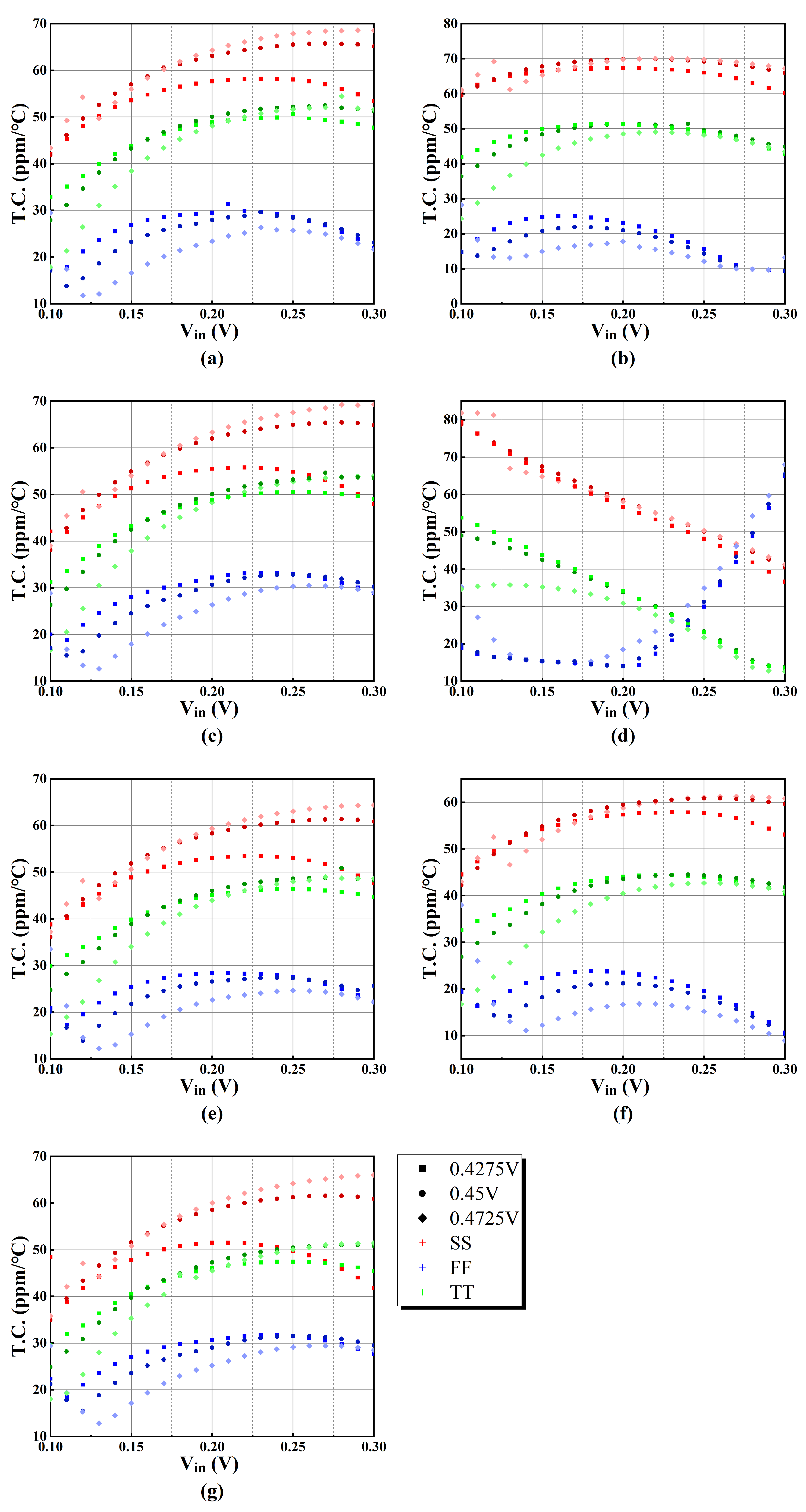
| VDD (V) | Process Corner | DC Gain (dB) | PM (°) | BW (Hz) | UGB (kHz) |
|---|---|---|---|---|---|
| 0.4275 | TT 1 | 66.6 | 82.29 | 19.95 | 65.45 |
| SS 2 | 67.75 | 79.06 | 13.94 | 51.58 | |
| FF 3 | 65.12 | 85.52 | 30.96 | 86.37 | |
| 0.45 | TT | 67.97 | 79.12 | 17.69 | 70.04 |
| SS | 69.2 | 75.34 | 12.23 | 55.13 | |
| FF | 66.53 | 82.76 | 27.43 | 93.07 | |
| 0.4725 | TT | 68.94 | 75.39 | 16.42 | 74.99 |
| SS | 70.2 | 71.08 | 11.29 | 58.84 | |
| FF | 67.49 | 79.55 | 25.45 | 100.1 |
| 1 | 2 | 3 | 4 | 5 | 6 | 7 | |
|---|---|---|---|---|---|---|---|
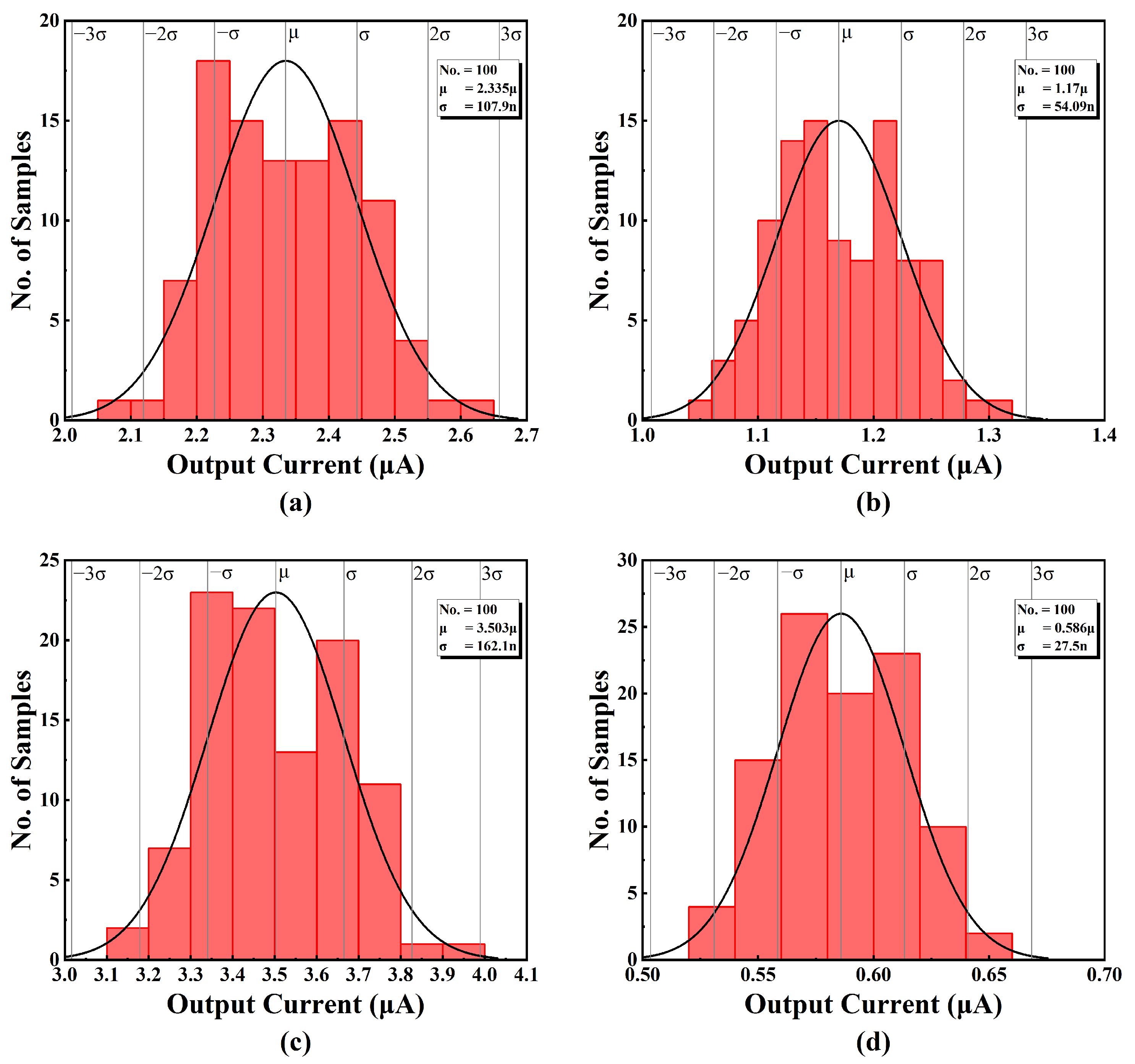
| μ (μA) | 2.335 | 1.17 | 3.503 | 0.586 | 2.92 | 1.755 | 4.087 |
| σ (nA) | 107.9 | 54.09 | 162.1 | 27.5 | 135.5 | 81.53 | 189.4 |
| Sensitivity of Output currents [(σ/μ)%] | 4.62 | 4.62 | 4.63 | 4.69 | 4.64 | 4.65 | 4.63 |
| VDD(V) | 0.4275 | 0.45 | 0.4725 | Overall | ||||
|---|---|---|---|---|---|---|---|---|
| T.C. (ppm/°C) | Min. | Max. | Min. | Max. | Min. | Max. | Min. | Max. |
| TT 1 | 13.56 | 53.83 | 13.80 | 54.68 | 12.60 | 62.11 | 12.60 | 62.11 |
| SS 2 | 36.72 | 79.48 | 34.97 | 78.78 | 35.88 | 81.85 | 34.97 | 81.85 |
| FF 3 | 9.33 | 64.95 | 9.43 | 65.39 | 8.88 | 68.03 | 8.88 | 68.03 |
| Min. | 9.33 | 9.43 | 8.88 | NA 4 | ||||
| Max. | 79.48 | 78.78 | 81.85 | NA | ||||
| 1 | 2 | 3 | 4 | 5 | 6 | 7 | |
|---|---|---|---|---|---|---|---|
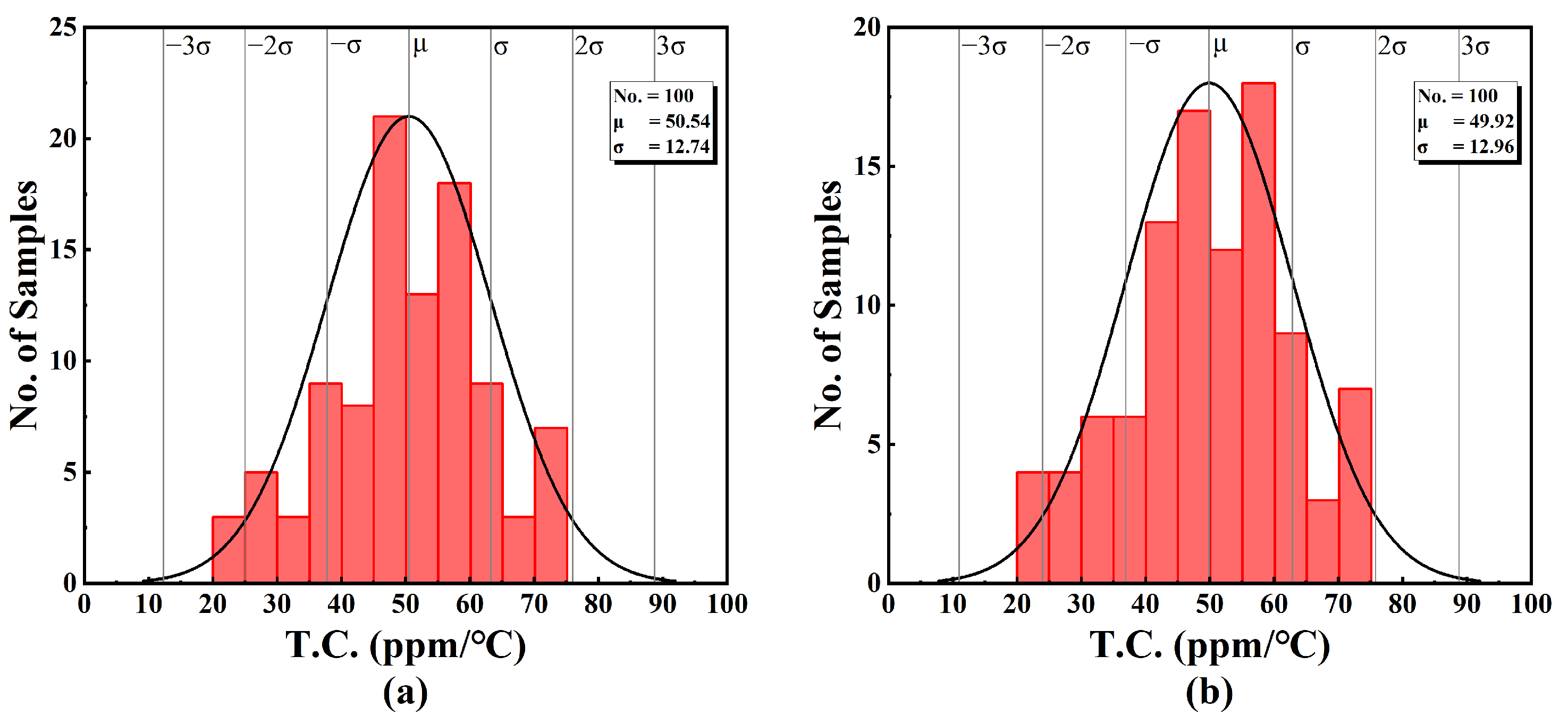
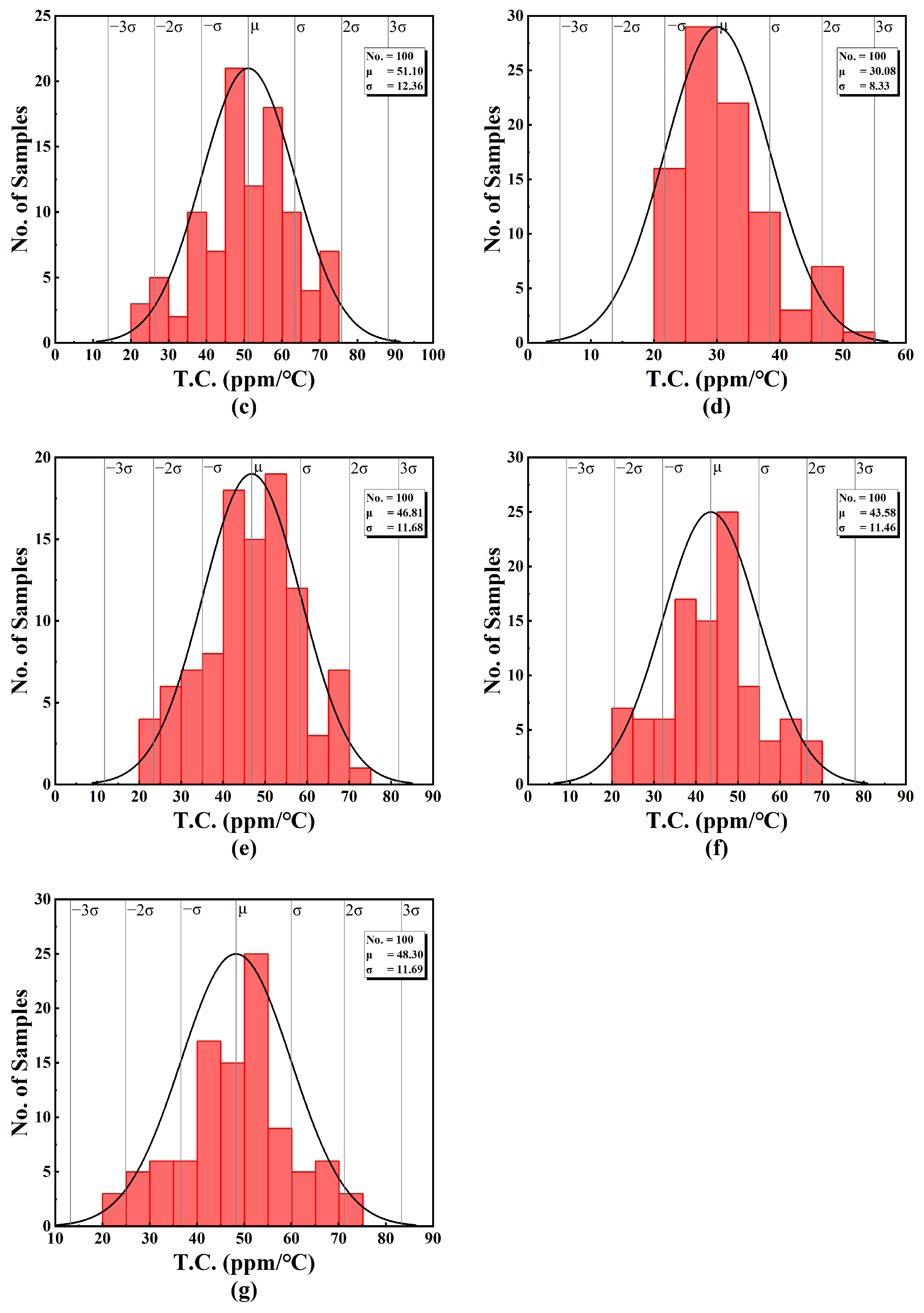
| μ (ppm/°C) | 50.54 | 49.92 | 51.10 | 30.08 | 46.81 | 43.58 | 48.30 |
| σ (ppm/°C) | 12.74 | 12.96 | 12.36 | 8.33 | 11.68 | 11.46 | 11.69 |
| Sensitivity of T.C. [(σ/μ)%] | 25.20 | 25.96 | 24.19 | 27.69 | 24.95 | 26.30 | 24.20 |
| 2001 [29] | 2007 [14] | 2013 [7] | 2019 [30] | 2020 [17] | This Work | |
|---|---|---|---|---|---|---|
| Technology (μm) | NA 1 | 0.5 | 0.18 | 0.18 | 0.13 | 0.04 |
| Supply voltage (V) | +1/−2 | ±1.5 | 1.2 | 0.3 | ±0.2 | 0.45 |
| Input range (V) | NA | 0–3 | 0–1.1 | 0–0.3 | −0.1–0.1 | 0.1–0.3 |
| Temperature range (°C) | 0–70 | NA | −40–120 | NA | NA | −20–80 |
| T.C. (ppm/°C) | 276 | NA | 113 | NA | NA | 54.68 |
| Power consumption (μW) | NA | 3000 | 85 | 0.01–0.1 | 0.36 | 0.36–2.76 |
| BW (Hz) | NA | 90 M | 14.1 M | 50–334 | 1.1 M | 34.45 k |
| PSRR (dB) | 46.2 | 35/43 | 47.8 | 50.2 | 52 | 45.58 |
| CMRR (dB) | NA | 62 | NA | 54.9 | 70 | 47.35 |
| Input referred noise [µV/sqrt(Hz)] | NA | 1.7 | 0.26 | 1.33 | 0.99 | 4.93 |
| THD (dB@Vpp@kHz) | NA | −60@6@100 | −44.2@1@100 | −46@0.1@0.1 | −41.61@0.1@10 | −56.66@0.1@1 |
| FOM {µW·[µV/sqrt(Hz)]/Hz} | NA | 5.67 × 10⁻⁷ | 1.56 × 10⁻⁶ | 3.98 × 10⁻⁴ | 3.24 × 10⁻⁷ | 5.15 × 10⁻⁵ |
Disclaimer/Publisher’s Note: The statements, opinions and data contained in all publications are solely those of the individual author(s) and contributor(s) and not of MDPI and/or the editor(s). MDPI and/or the editor(s) disclaim responsibility for any injury to people or property resulting from any ideas, methods, instructions or products referred to in the content. |
© 2025 by the authors. Licensee MDPI, Basel, Switzerland. This article is an open access article distributed under the terms and conditions of the Creative Commons Attribution (CC BY) license (https://creativecommons.org/licenses/by/4.0/).
Share and Cite
Chen, H.; Chan, P.K. A Low-Voltage Low-Power Voltage-to-Current Converter with Low Temperature Coefficient Design Awareness. Sensors 2025, 25, 1204. https://doi.org/10.3390/s25041204
Chen H, Chan PK. A Low-Voltage Low-Power Voltage-to-Current Converter with Low Temperature Coefficient Design Awareness. Sensors. 2025; 25(4):1204. https://doi.org/10.3390/s25041204
Chicago/Turabian StyleChen, Haoze, and Pak Kwong Chan. 2025. "A Low-Voltage Low-Power Voltage-to-Current Converter with Low Temperature Coefficient Design Awareness" Sensors 25, no. 4: 1204. https://doi.org/10.3390/s25041204
APA StyleChen, H., & Chan, P. K. (2025). A Low-Voltage Low-Power Voltage-to-Current Converter with Low Temperature Coefficient Design Awareness. Sensors, 25(4), 1204. https://doi.org/10.3390/s25041204