
Design and Optimization of a Gold and Silver Nanoparticle-Based SERS Biosensing Platform

Abstract
1. Introduction
2. Materials and Methods
2.1. Materials
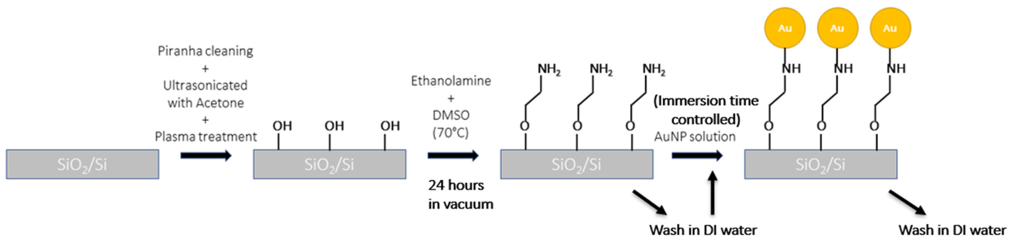
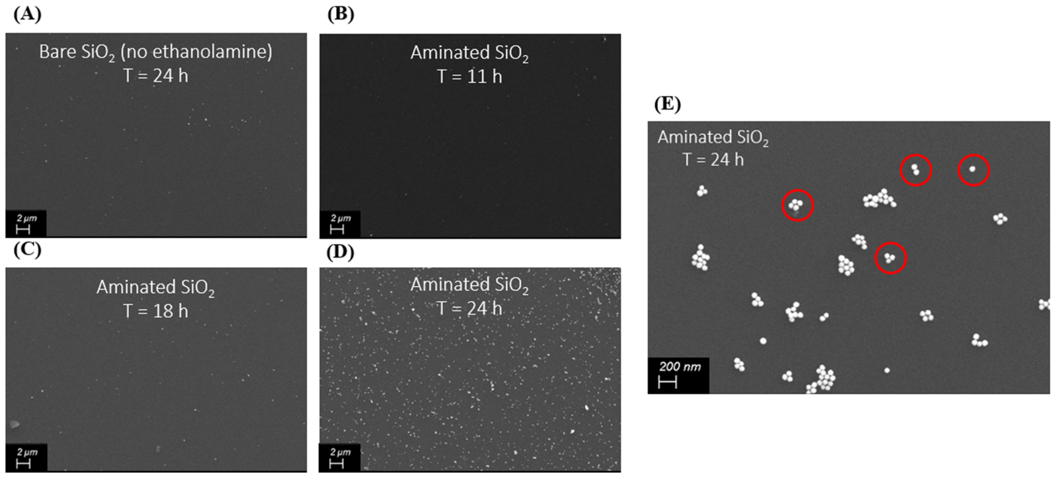
2.2. Fabrication
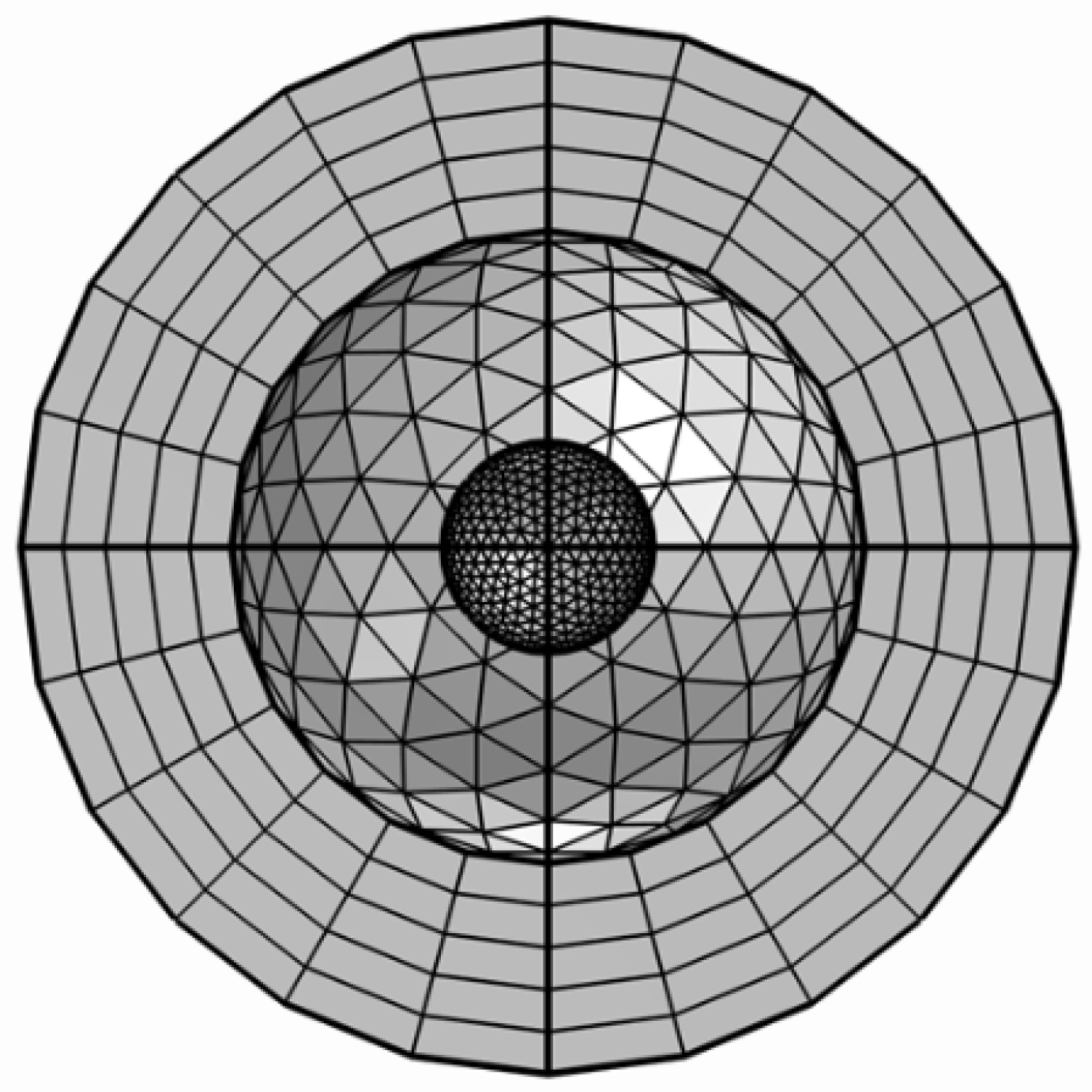
2.3. Simulations
3. Results and Discussion
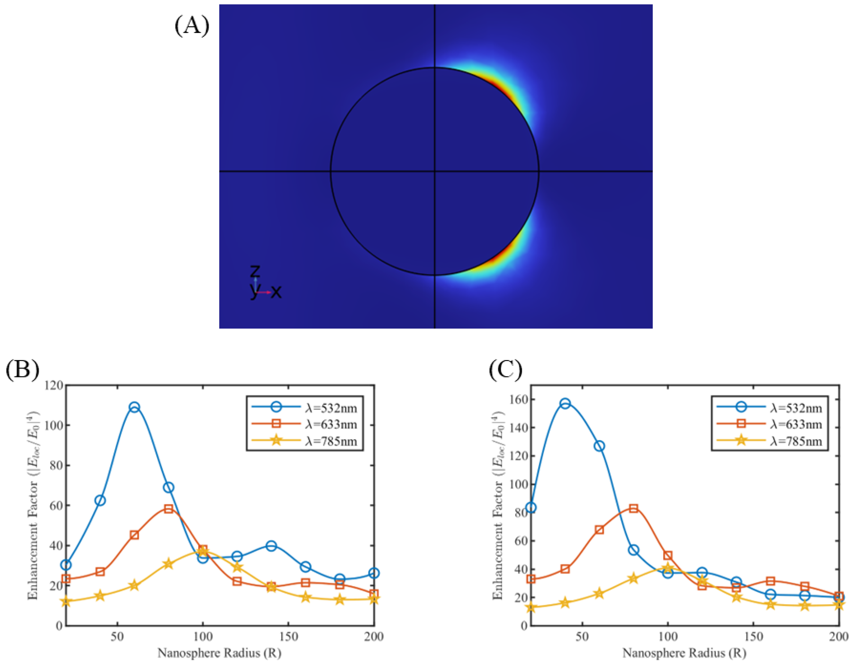
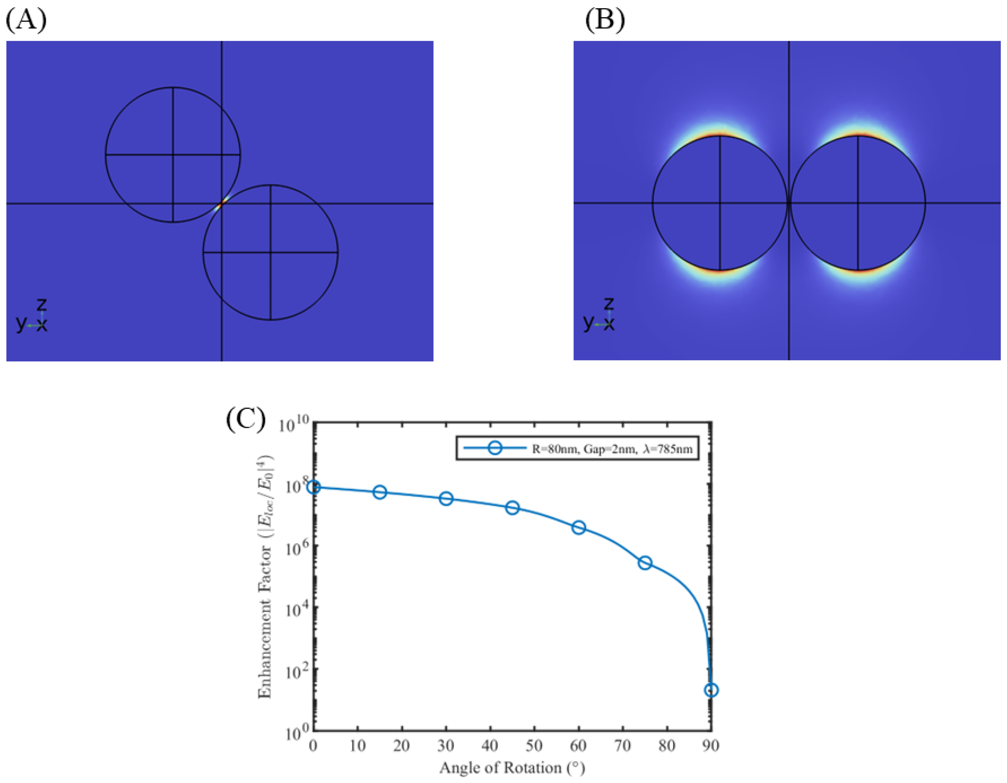
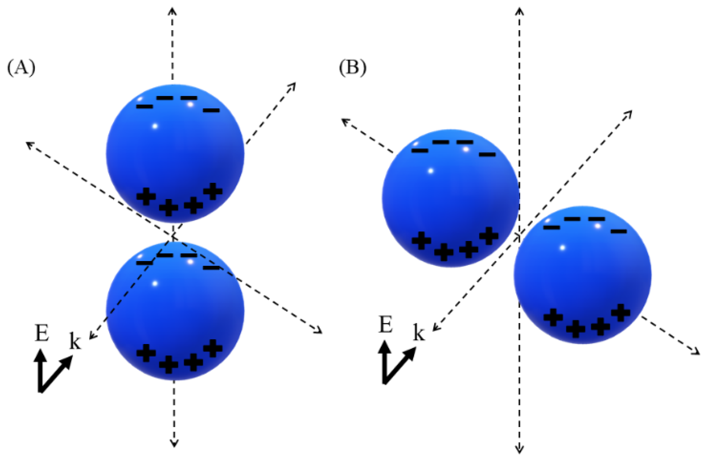
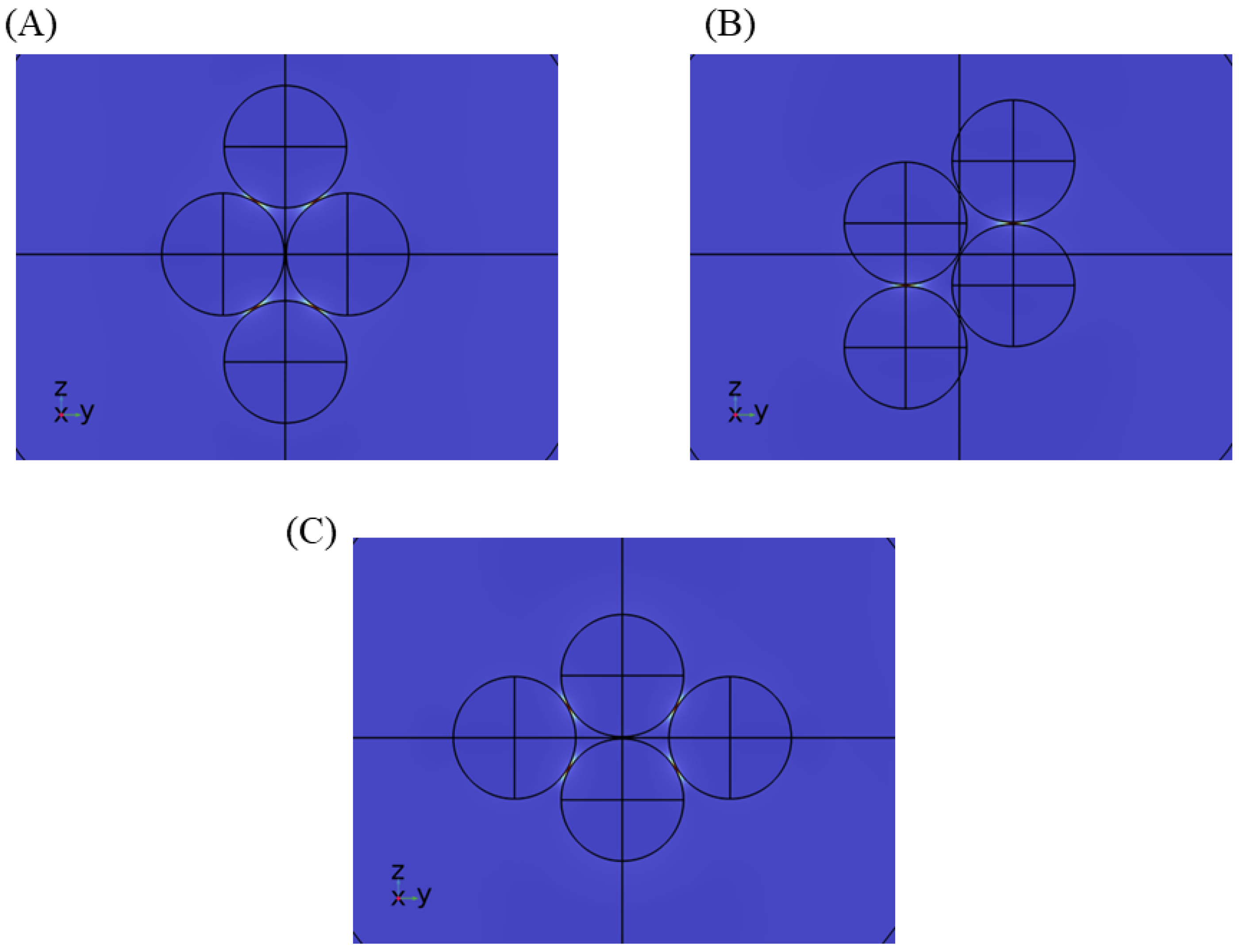
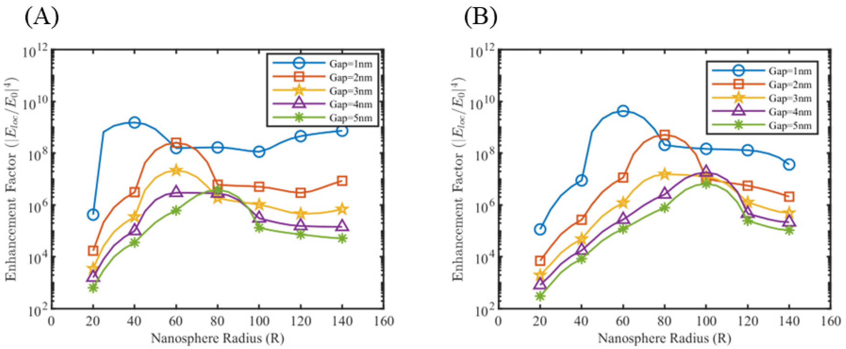
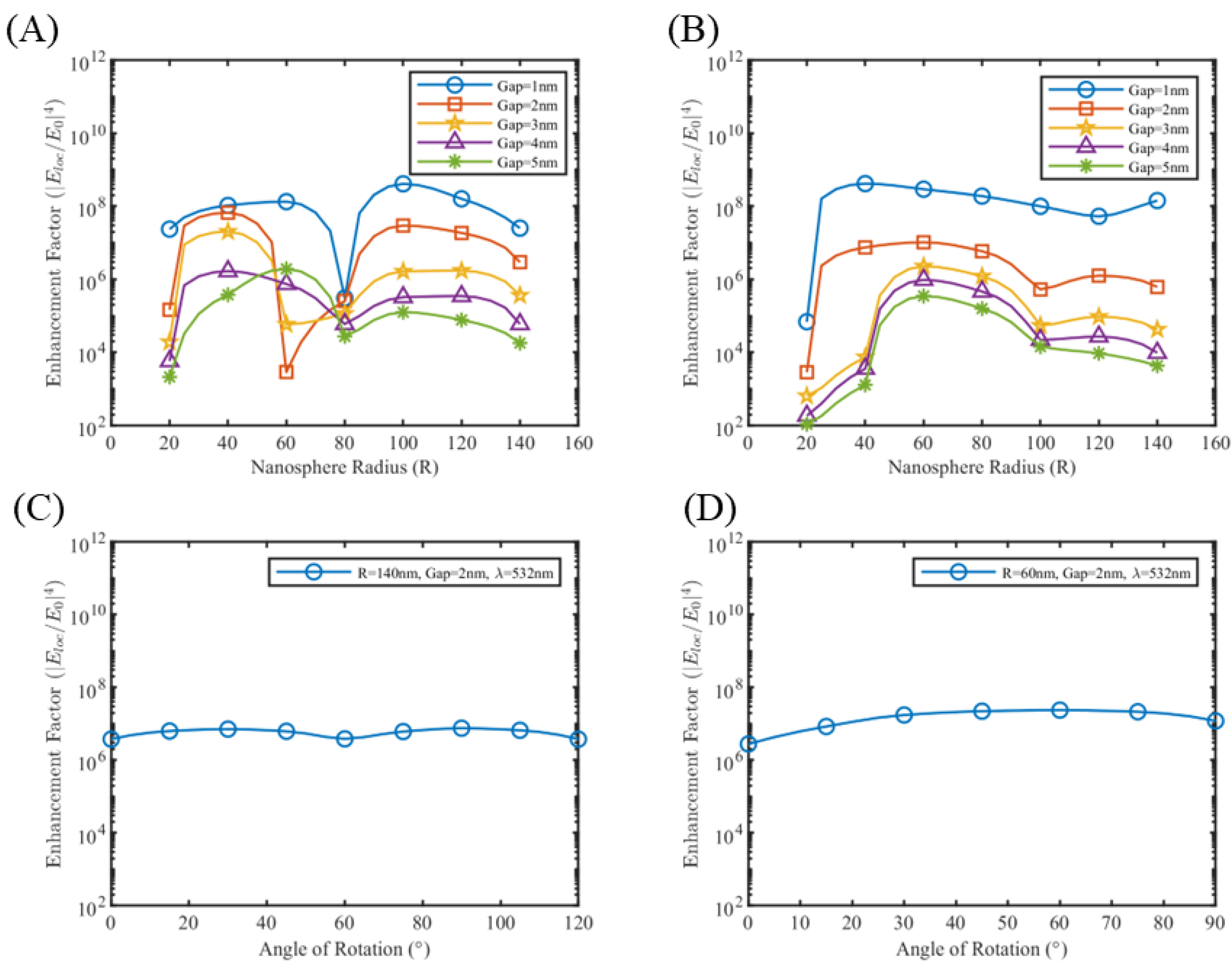
3.1. Near Field Simulations and Optimization of Nanoparticle Systems
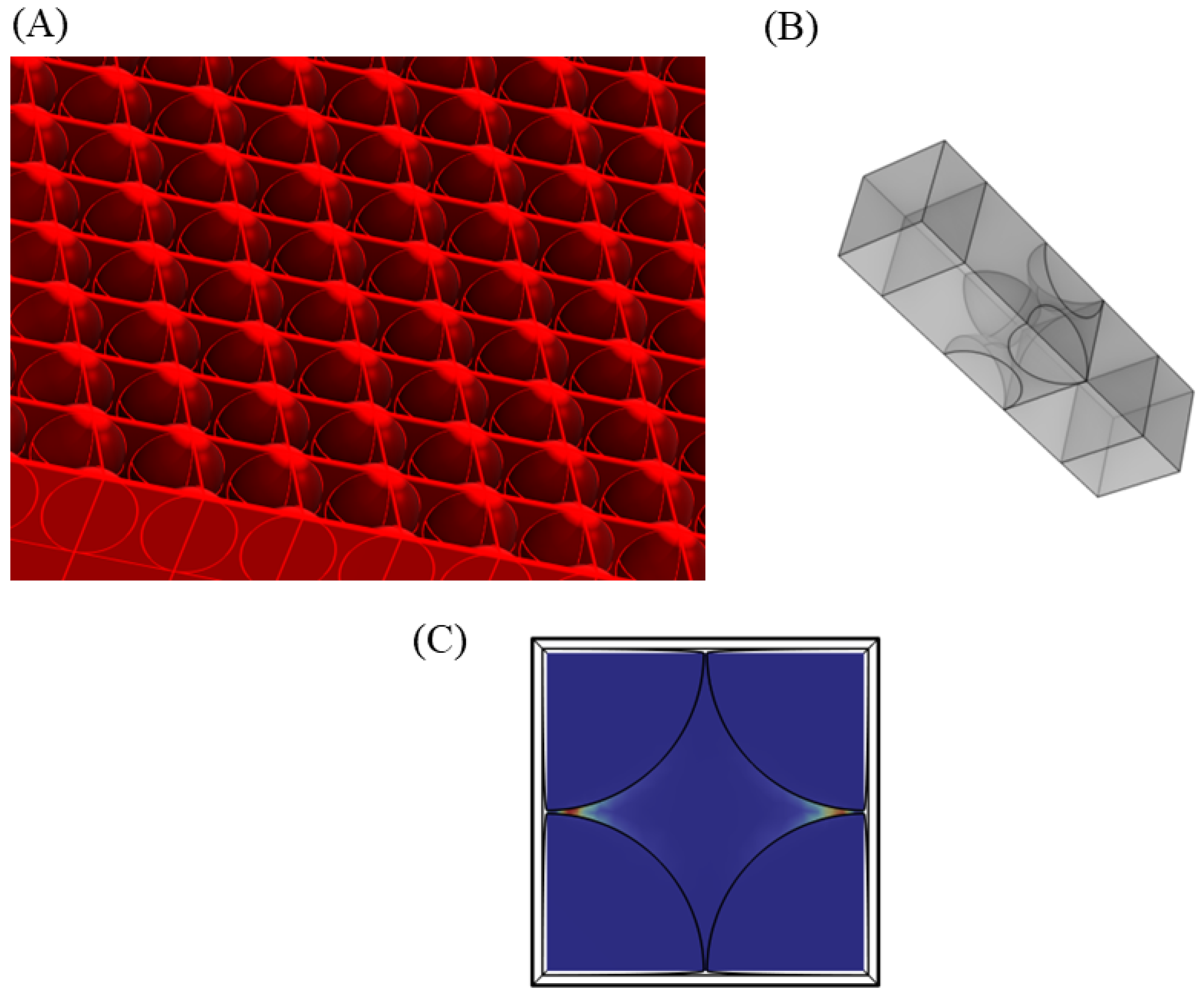
3.2. Near Field Simulations and Optimization of Periodic Nanoparticle Array
3.3. Limitation of the Model
3.4. Raman Spectroscopy with Raman Probe Molecule
4. Conclusions
Supplementary Materials
Author Contributions
Funding
Institutional Review Board Statement
Informed Consent Statement
Data Availability Statement
Acknowledgments
Conflicts of Interest
References
- McCreery, R.L. Raman Spectroscopy for Chemical Analysis; John Wiley & Sons: Hoboken, NJ, USA, 2005. [Google Scholar]
- Mosier-Boss, P.A. Review of SERS substrates for chemical sensing. Nanomaterials 2017, 7, 142. [Google Scholar] [CrossRef]
- Lee, W.; Lee, S.Y.; Briber, R.M.; Rabin, O. Self-assembled SERS substrates with tunable surface plasmon resonances. Adv. Funct. Mater. 2011, 21, 3424–3429. [Google Scholar] [CrossRef]
- Li, W.; Camargo, P.H.C.; Lu, X.; Xia, Y. Dimers of silver nanospheres: Facile synthesis and their use as hot spots for surface-enhanced Raman scattering. Nano Lett. 2009, 9, 485–490. [Google Scholar] [CrossRef] [PubMed]
- Joseph, V.; Matschulat, A.; Polte, J.; Rolf, S.; Emmerling, F.; Kneipp, J. SERS enhancement of gold nanospheres of defined size. J. Raman Spectrosc. 2011, 42, 1736–1742. [Google Scholar] [CrossRef]
- Ponlamuangdee, K.; Hornyak, G.L.; Bora, T.; Bamrungsap, S. Graphene oxide/gold nanorod plasmonic paper—A simple and cost-effective SERS substrate for anticancer drug analysis. New J. Chem. 2020, 44, 14087–14094. [Google Scholar] [CrossRef]
- Dong, J.; Qi, J.; Li, H.; Li, J.; Wang, R.; Fang, Y.; Li, X. Nanoscale vertical arrays of gold nanorods by self-assembly: Physical mechanism and application. Nanoscale Res. Lett. 2019, 14, 118. [Google Scholar] [CrossRef] [PubMed]
- Zhang, J.; Irannejad, M.; Cui, B. Bowtie nanoantenna with single-digit nanometer gap for surface-enhanced Raman scattering (SERS). Plasmonics 2015, 10, 831–837. [Google Scholar] [CrossRef]
- Hatab, N.A.; Rouleau, C.M.; Retterer, S.T.; Eres, G.; Hatzinger, P.B.; Gu, B. An integrated portable Raman sensor with nanofabricated gold bowtie array substrates for energetics detection. Analyst 2011, 136, 1697–1702. [Google Scholar] [CrossRef] [PubMed]
- Jalali, M.; Hosseini, I.I.; AbdelFatah, T.; Montermini, L.; Hogiu, S.W.; Rak, J.; Mahshid, S. Plasmonic nanobowtiefluidic device for sensitive detection of glioma extracellular vesicles by Raman spectrometry. Lab Chip 2021, 21, 855–866. [Google Scholar] [CrossRef]
- Liebig, F.; Henning, R.; Sarhan, R.M.; Prietzel, C.; Bargheer, M.; Koetz, J. A new route to gold nanoflowers. Nanotechnology 2018, 29, 185603. [Google Scholar] [CrossRef] [PubMed]
- Zheng, D.; Pisano, F.; Collard, L.; Balena, A.; Pisanello, M.; Spagnolo, B.; Mach-Batlle, R.; Tantussi, F.; Carbone, L.; De Angelis, F.; et al. Toward Plasmonic Neural Probes: SERS Detection of Neurotransmitters through Gold-Nanoislands-Decorated Tapered Optical Fibers with Sub-10 nm Gaps. Adv. Mater. 2023, 35, 2200902. [Google Scholar] [CrossRef]
- LimLim, H.; Kim, D.; Kwon, G.; Kim, H.-J.; You, J.; Kim, J.; Eguchi, M.; Nanjundan, A.K.; Na, J.; Yamauchi, Y. Synthesis of uniformly sized mesoporous silver films and their SERS application. J. Phys. Chem. C 2020, 124, 23730–23737. [Google Scholar] [CrossRef]
- Karn-Orachai, K. Gap-dependent surface-enhanced Raman scattering (SERS) enhancement model of SERS substrate–probe combination using a polyelectrolyte nanodroplet as a distance controller. Langmuir 2021, 37, 10776–10785. [Google Scholar] [CrossRef]
- Benz, F.; Chikkaraddy, R.; Salmon, A.; Ohadi, H.; De Nijs, B.; Mertens, J.; Carnegie, C.; Bowman, R.W.; Baumberg, J.J. SERS of individual nanoparticles on a mirror: Size does matter, but so does shape. J. Phys. Chem. Lett. 2016, 7, 2264–2269. [Google Scholar] [CrossRef]
- Sugawa, K.; Akiyama, T.; Tanoue, Y.; Harumoto, T.; Yanagida, S.; Yasumori, A.; Tomita, S.; Otsuki, J. Particle size dependence of the surface-enhanced Raman scattering properties of densely arranged two-dimensional assemblies of Au(core)–Ag(shell) nanospheres. Phys. Chem. Chem. Phys. 2014, 17, 21182–21189. [Google Scholar] [CrossRef] [PubMed]
- Pilot, R.; Massari, M. Silver nanoparticle aggregates: Wavelength dependence of their SERS properties in the first transparency window of biological tissues. Chem. Phys. Impact 2021, 2, 100014. [Google Scholar] [CrossRef]
- COMSOL Multiphysics® Software. Available online: https://www.comsol.com/wave-optics-module (accessed on 5 March 2023).
- Jin, J.M. The Finite Element Method in Electromagnetics; John Wiley & Sons: Hoboken, NJ, USA, 2015. [Google Scholar]
- Saini, R.K.; Sharma, A.K.; Agarwal, A.; Prajesh, R. Near field FEM simulations of plasmonic gold nanoparticle based SERS substrate with experimental validation. Mater. Chem. Phys. 2022, 287, 126288. [Google Scholar] [CrossRef]
- McMahon, J.M.; Henry, A.I.; Wustholz, K.L.; Natan, M.J.; Freeman, R.G.; Van Duyne, R.P.; Schatz, G.C. Gold nanoparticle dimer plasmonics: Finite element method calculations of the electromagnetic enhancement to surface-enhanced Raman spectroscopy. Anal. Bioanal. Chem. 2009, 394, 1819–1825. [Google Scholar] [CrossRef] [PubMed]
- Micic, M.; Klymyshyn, N.; Suh, Y.D.; Lu, H.P. Finite element method simulation of the field distribution for AFM tip-enhanced surface-enhanced Raman scanning microscopy. J. Phys. Chem. B 2003, 107, 1574–1584. [Google Scholar] [CrossRef]
- Gu, Z.; Wang, J.; Miao, B.; Zhao, L.; Liu, X.; Wu, D.; Li, J. Highly sensitive AlGaN/GaN HEMT biosensors using an ethanolamine modification strategy for bioassay applications. RSC Adv. 2019, 9, 15341–15349. [Google Scholar] [CrossRef] [PubMed]
- Ebner, A.; Hinterdorfer, P.; Gruber, H.J. Comparison of different aminofunctionalization strategies for attachment of single antibodies to AFM cantilevers. Ultramicroscopy 2007, 107, 922–927. [Google Scholar] [CrossRef] [PubMed]
- Rakić, A.D.; Djurišić, A.B.; Elazar, J.M.; Majewski, M.L. Optical properties of metallic films for vertical-cavity optoelectronic devices. Appl. Opt. 1998, 37, 5271–5283. [Google Scholar] [CrossRef]
- Le Ru, E.C.; Etchegoin, P.G. Quantifying SERS enhancements. MRS Bull. 2013, 38, 631–640. [Google Scholar] [CrossRef]
- Nie, S.; Emory, S.R. Probing single molecules and single nanoparticles by surface-enhanced Raman scattering. Science 1997, 275, 1102–1106. [Google Scholar] [CrossRef] [PubMed]
- Kneipp, K.; Wang, Y.; Kneipp, H.; Perelman, L.T.; Itzkan, I.; Dasari, R.R.; Feld, M.S. Single molecule detection using surface-enhanced Raman scattering (SERS). Phys. Rev. Lett. 1997, 78, 1667. [Google Scholar] [CrossRef]
- Hao, F.; Nordlander, P. Plasmonic coupling between a metallic nanosphere and a thin metallic wire. Appl. Phys. Lett. 2006, 89, 103101. [Google Scholar] [CrossRef]
- Knorr, I.; Christou, K.; Meinertz, J. Prediction and Optimization of Surface-Enhanced Raman Scattering Geometries using COMSOL Multiphysics. In Proceedings of the COMSOL Conference, Hannover, Germany, 4–6 November 2008. [Google Scholar]
- Le Ru, E.C.; Blackie, E.; Meyer, M.; Etchegoin, P.G. Surface enhanced Raman scattering enhancement factors: A comprehensive study. J. Phys. Chem. C 2007, 111, 13794–13803. [Google Scholar] [CrossRef]
- Ciou, S.H.; Cao, Y.W.; Huang, H.C.; Su, D.Y.; Huang, C.L. SERS enhancement factors studies of silver nanoprism and spherical nanoparticle colloids in the presence of bromide ions. J. Phys. Chem. C 2009, 113, 9520–9525. [Google Scholar] [CrossRef]
- Le Ru, E.C.; Etchegoin, P.G. Principles of Surface-Enhanced Raman Spectroscopy; Elsevier: Amsterdam, The Netherlands, 2009. [Google Scholar]
- Jin, C.; Du, Z.; Liu, C.; Liu, F.; Hu, J.; Han, M. Two orders of magnitude extra SERS enhancement on silver nanoparticle-based substrate induced by laser irradiation in nitrogen ambient. Spectrochim. Acta Part A Mol. Biomol. Spectrosc. 2022, 265, 120372. [Google Scholar] [CrossRef] [PubMed]
- Yang, Y.; Matsubara, S.; Xiong, L.; Hayakawa, T.; Nogami, M. Solvothermal synthesis of multiple shapes of silver nanoparticles and their SERS properties. J. Phys. Chem. C 2007, 111, 9095–9104. [Google Scholar] [CrossRef]
- He, R.X.; Liang, R.; Peng, P.; Norman Zhou, Y. Effect of the size of silver nanoparticles on SERS signal enhancement. J. Nanoparticle Res. 2017, 19, 267. [Google Scholar] [CrossRef]
- Huang, J.; Zhang, L.; Chen, B.; Ji, N.; Chen, F.; Zhang, Y.; Zhang, Z. Nanocomposites of size-controlled gold nanoparticles and graphene oxide: Formation and applications in SERS and catalysis. Nanoscale 2010, 2, 2733–2738. [Google Scholar] [CrossRef] [PubMed]
- Szekeres, G.P.; Kneipp, J. SERS probing of proteins in gold nanoparticle agglomerates. Front. Chem. 2019, 7, 30. [Google Scholar] [CrossRef] [PubMed]
- Green, M.A. Self-consistent optical parameters of intrinsic silicon at 300 K including temperature coefficients. Sol. Energy Mater. Sol. Cells 2008, 92, 1305–1310. [Google Scholar] [CrossRef]
- Mao, L.; Li, Z.; Wu, B.; Xu, H. Effects of quantum tunneling in metal nanogap on surface-enhanced Raman scattering. Appl. Phys. Lett. 2009, 94, 243102. [Google Scholar] [CrossRef]
- OriginLab. Origin: Data Analysis and Graphing Software. Available online: https://www.originlab.com/index.aspx?go=Products/Origin#Data_Analysis_and_Statistics (accessed on 15 March 2023).
- Xiao, G.N.; Man, S.Q. Surface-enhanced Raman scattering of methylene blue adsorbed on cap-shaped silver nanoparticles. Chem. Phys. Lett. 2007, 447, 305–309. [Google Scholar] [CrossRef]
- Ruan, C.; Wang, W.; Gu, B. Single-molecule detection of thionine on aggregated gold nanoparticles by surface enhanced Raman scattering. J. Raman Spectrosc. 2007, 38, 568–573. [Google Scholar] [CrossRef]
- Saha, S. A Simulation Study of Nanoparticle-Based SERS Biosensing Platform with Application Towards Glioma Detection. Master’s Thesis, University of Waterloo, Waterloo, ON, Canada, 2023. [Google Scholar]


Disclaimer/Publisher’s Note: The statements, opinions and data contained in all publications are solely those of the individual author(s) and contributor(s) and not of MDPI and/or the editor(s). MDPI and/or the editor(s) disclaim responsibility for any injury to people or property resulting from any ideas, methods, instructions or products referred to in the content. |
© 2025 by the authors. Licensee MDPI, Basel, Switzerland. This article is an open access article distributed under the terms and conditions of the Creative Commons Attribution (CC BY) license (https://creativecommons.org/licenses/by/4.0/).
Share and Cite
Saha, S.; Sachdev, M.; Mitra, S.K. Design and Optimization of a Gold and Silver Nanoparticle-Based SERS Biosensing Platform. Sensors 2025, 25, 1165. https://doi.org/10.3390/s25041165
Saha S, Sachdev M, Mitra SK. Design and Optimization of a Gold and Silver Nanoparticle-Based SERS Biosensing Platform. Sensors. 2025; 25(4):1165. https://doi.org/10.3390/s25041165
Chicago/Turabian StyleSaha, Soumyadeep, Manoj Sachdev, and Sushanta K. Mitra. 2025. "Design and Optimization of a Gold and Silver Nanoparticle-Based SERS Biosensing Platform" Sensors 25, no. 4: 1165. https://doi.org/10.3390/s25041165
APA StyleSaha, S., Sachdev, M., & Mitra, S. K. (2025). Design and Optimization of a Gold and Silver Nanoparticle-Based SERS Biosensing Platform. Sensors, 25(4), 1165. https://doi.org/10.3390/s25041165