1. Introduction
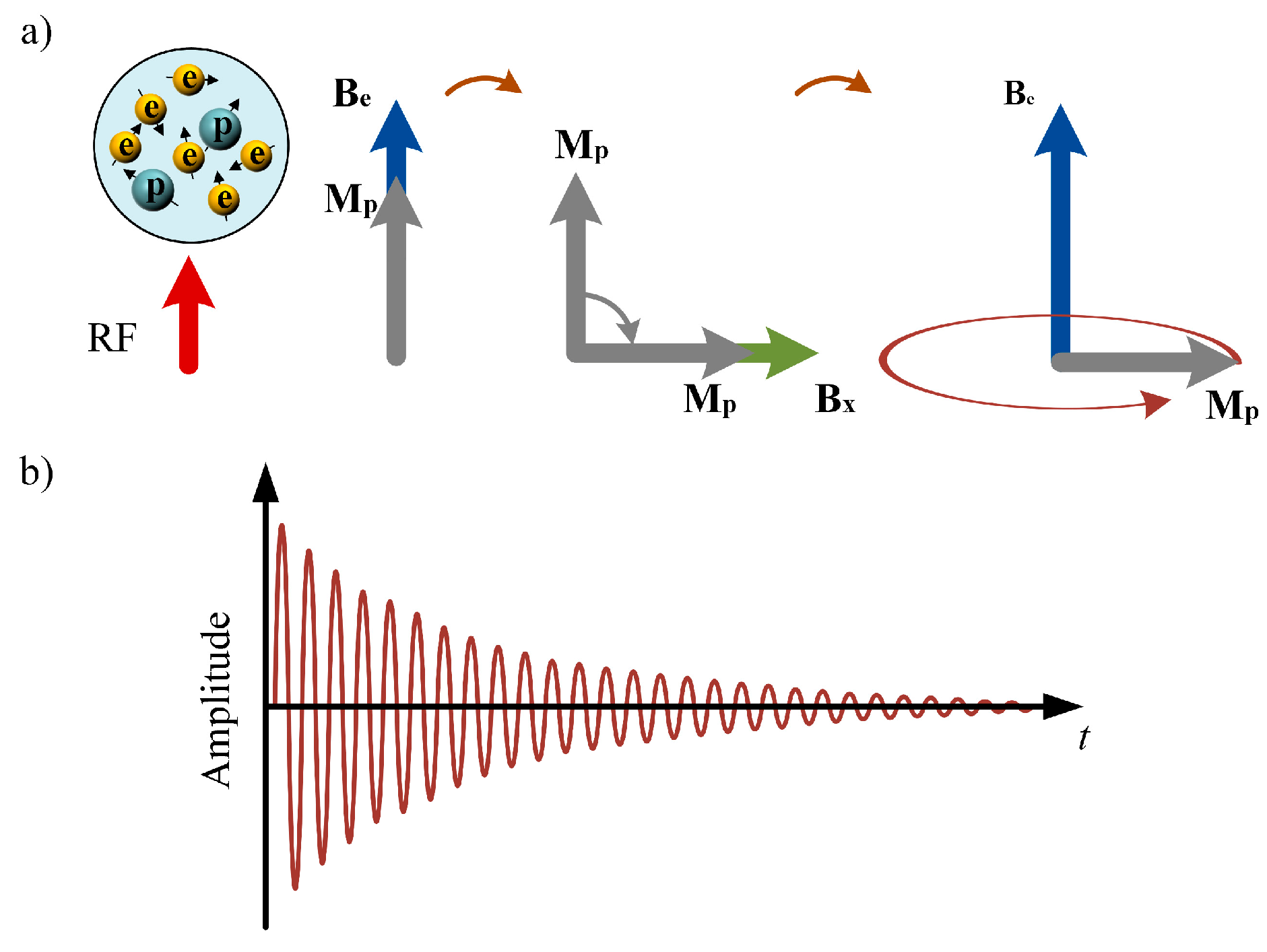
The Overhauser magnetometer (OVM) is a proton precession magnetometer which uses electron–nuclear double resonance to enhance the proton polarization [
1]. Its polarization strength is dozens of times higher than that of traditional proton magnetometers [
2]. Due to its advantages, such as low power, high sensitivity, high absolute accuracy, excellent portability, and stable performance, the OVM has been widely used in many fields such as geomagnetic field measurement, magnetic target detection, and magnetic device calibration [
3,
4,
5,
6].
Sensitivity is a key indicator of the OVM, representing the statistical uncertainty observed during repeated measurements of the same magnetic field [
7]. It reflects the instrument’s measurement noise, which is primarily determined by the signal-to-noise ratio (SNR) of the Larmor signal [
8]. To improve sensitivity, previous research has mainly focused on two aspects: FID signal processing and hardware optimization.
In terms of signal processing, the primary research focus is on suppressing different types of noise embedded in the free induction decay (FID) signal [
9]. Tan et al. [
10] proposed an optimal multi-average (OMAM) frequency measurement algorithm that achieved a sensitivity of 0.2 nT/
, effectively enhancing frequency precision. Wang et al. [
11] introduced a segmented linear regression method to recover FID signals suppressed by saturation, thereby improving signal stability. Luo et al. [
12] further proposed an intelligent full-wavenumber fitting algorithm for low-SNR FID signals, achieving 0.067 nT sensitivity and strong robustness against interference. These studies significantly improved frequency extraction accuracy but mainly focused on algorithmic optimization, without analyzing the intrinsic noise sources that fundamentally limit sensitivity.
In terms of hardware, Liu et al. [
13] developed an adjustable tuning–matching framework that broadened the sensing coil bandwidth and reduced the noise floor, effectively doubling the SNR and sensitivity under strong interference. Wang et al. [
14] designed an integrated dual-mode magnetometer with a sensitivity better than 0.06 nT, demonstrating high precision and system stability. Commercial OVMs, such as those produced by GEM Systems (Canada), have already achieved sensitivities of approximately 0.01 nT.
However, these works primarily addressed circuit filtering optimization and external interference suppression, while the intrinsic noise mechanisms within the sensor and circuit remain insufficiently investigated. By contrast, other weak magnetic field sensing technologies have developed more mature and systematic noise analyses. In magnetoresistive (MR) heads, thermal magnetization fluctuations have been identified as a fundamental white-noise limit that scales inversely with sensor volume [
15]. Giant magnetoimpedance (GMI) wires and multilayer thin films have been shown to exhibit intrinsic magnetic noise governed by magnetization dynamics, anisotropy, and damping, with equivalent noise reaching the sub-nT to pT/
range [
16,
17]. Magnetic tunnel junction (MTJ) magnetometers have further established unified equivalent-noise models that incorporate sensor, front-end electronics, and feedback-coil contributions, with the latter often dominating at low frequencies [
18]. These studies highlight the well-developed understanding of intrinsic noise in sensors, whereas intrinsic noise in the OVM remains relatively unexplored.
The study of the inherent noise characteristics of the OVM helps us understand the composition of noise sources and the contributions of various noise sources, and this is important for intrinsic noise suppression and SNR enhancement in order to obtain high sensitivity. For this purpose, an equivalent noise model for OVM is established, and the optimized sensor parameters according to this noise model are used to obtain a high SNR Larmor signal, hence the high sensitivity. First, a comprehensive noise model combined with the sensor and the receiving circuit is proposed to analyze the impact of various types of noise on the SNR of the FID signal. Second, the influence of circuit transmission characteristics on noise is investigated, and the noise transmission characteristics are obtained, and the influence of various electrical parameters of the sensor and circuit on the noise was analyzed. Finally, the correctness of the noise model was verified, and the sensitivity under low instrument background noise was estimated, experimentally. The main contributions of this work are as follows:
- (1)
A comprehensive noise model is developed to describe the intrinsic noise sources within the OVM, including sensor noise and circuit noise.
- (2)
The proposed noise model is used to guide the optimization of sensor parameters and circuit design, effectively reducing the total output noise and improving the SNR.
- (3)
The accuracy of the proposed model and the sensitivity of the optimized OVM are experimentally verified. The results confirm that the developed noise model can accurately reflect system noise behavior and provide theoretical guidance for low-noise design.
Therefore, this study aims to construct a comprehensive quantitative noise model for the OVM, systematically identifying both intrinsic physical noise sources and circuit-induced noise pathways. By resolving the noise contributions of each stage in the analog and validating them through dedicated experiments, the study offers practical design guidance for improving its SNR performance.
3. Analytical Noise Model of OVMs
The audio coil, as an electromagnetic induction sensor, can operate under various conditions, including critical damping in time-domain induction, resonance in frequency-domain induction, and negative feedback in broadband induction. In this work, the OVM operates in the resonant state of frequency-domain induction. By modeling the coil noise under this resonant condition, the coil parameters can be optimized to enhance the system performance and suppress excessive inherent noise.
3.1. Noise Model of the Audio Coil and Preamplifier
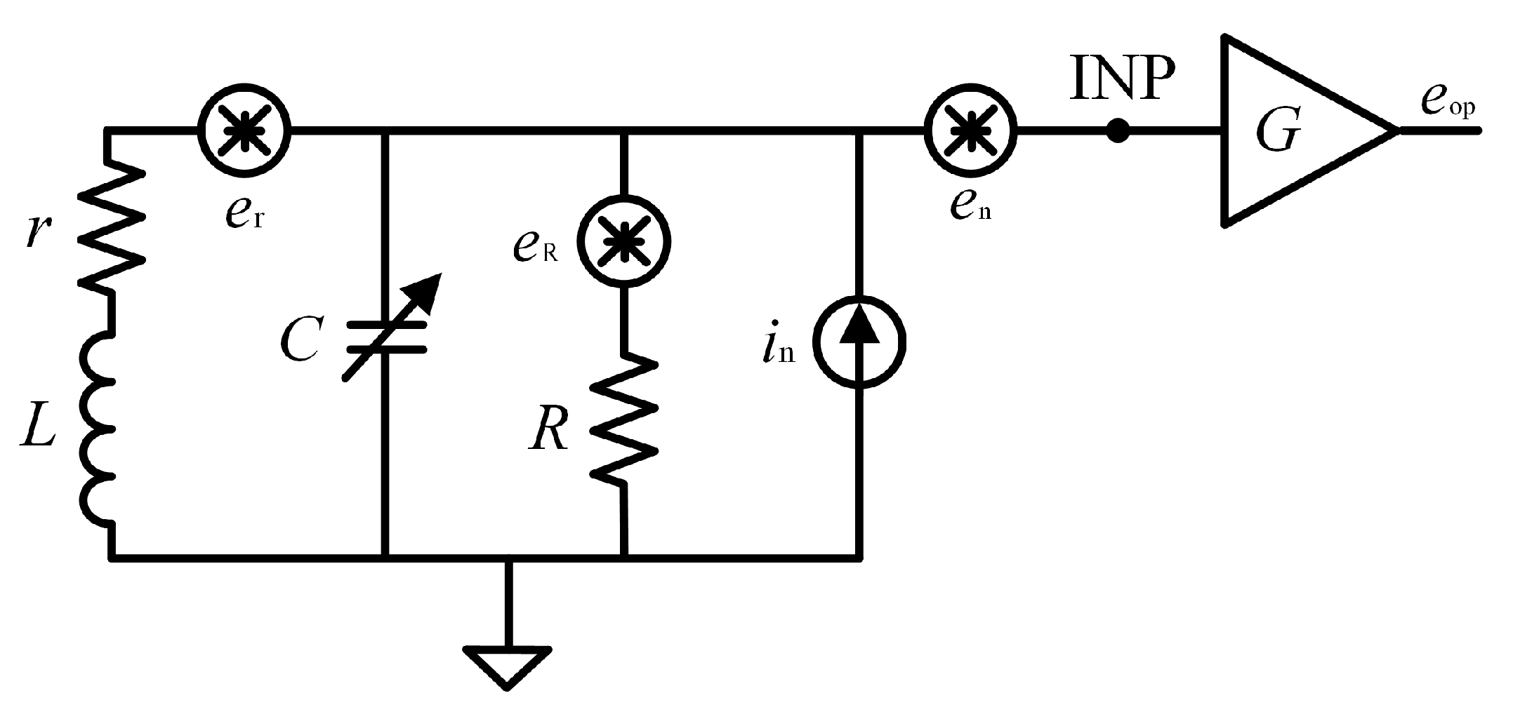
As shown in
Figure 3, the sensor coil can be equivalent to a series circuit model composed of inductance
L and resistance
r, and a tuning capacitor
C is connected in parallel to the sensor coil, which forms an LC resonant circuit, where
R is the matching resistor that determines the
Q of the circuit, and
G is the gain of the preamplifier.
The thermal noise spectral density of the audio coil resistance contribution
er is
where
k is the Boltzmann constant, and
T is the temperature. The contribution of
er to the noise at the preamplifier input node INP is
where
is the angular frequency of LC resonance and is
The thermal noise spectral density of the matching resistor contribution
eR is
The contribution of the matching resistor thermal noise
eR to the noise at the preamplifier input node INP is
The voltage noise of the preamplifier presents 1/f noise in the low-frequency band, and the noise corner frequency usually occurs at several Hz. The measurement range of the OVM is 851 Hz to 5109 Hz, so in this frequency band, the voltage noise en can be regarded as a constant, and its contribution to the noise of the preamplifier input node is also en.
The current noise
in of the preamplifier represents current fluctuations at the input of an otherwise noise-free amplifier with open inputs and can be expressed as
The total noise at the preamplifier output is
Considering (4)–(10),
is simplified as
According to (11), we can see that the audio coil resistor thermal noise, the matching resistor thermal noise, and current noise are mainly affected by the resonant circuit, and their spectral densities reach a maximum at the resonance point and gradually decrease away from the resonance point. The voltage noise spectral density of the preamplifier, on the other hand, is not affected by the resonant circuit.
3.2. Impact of Transmission Characteristics on Noise
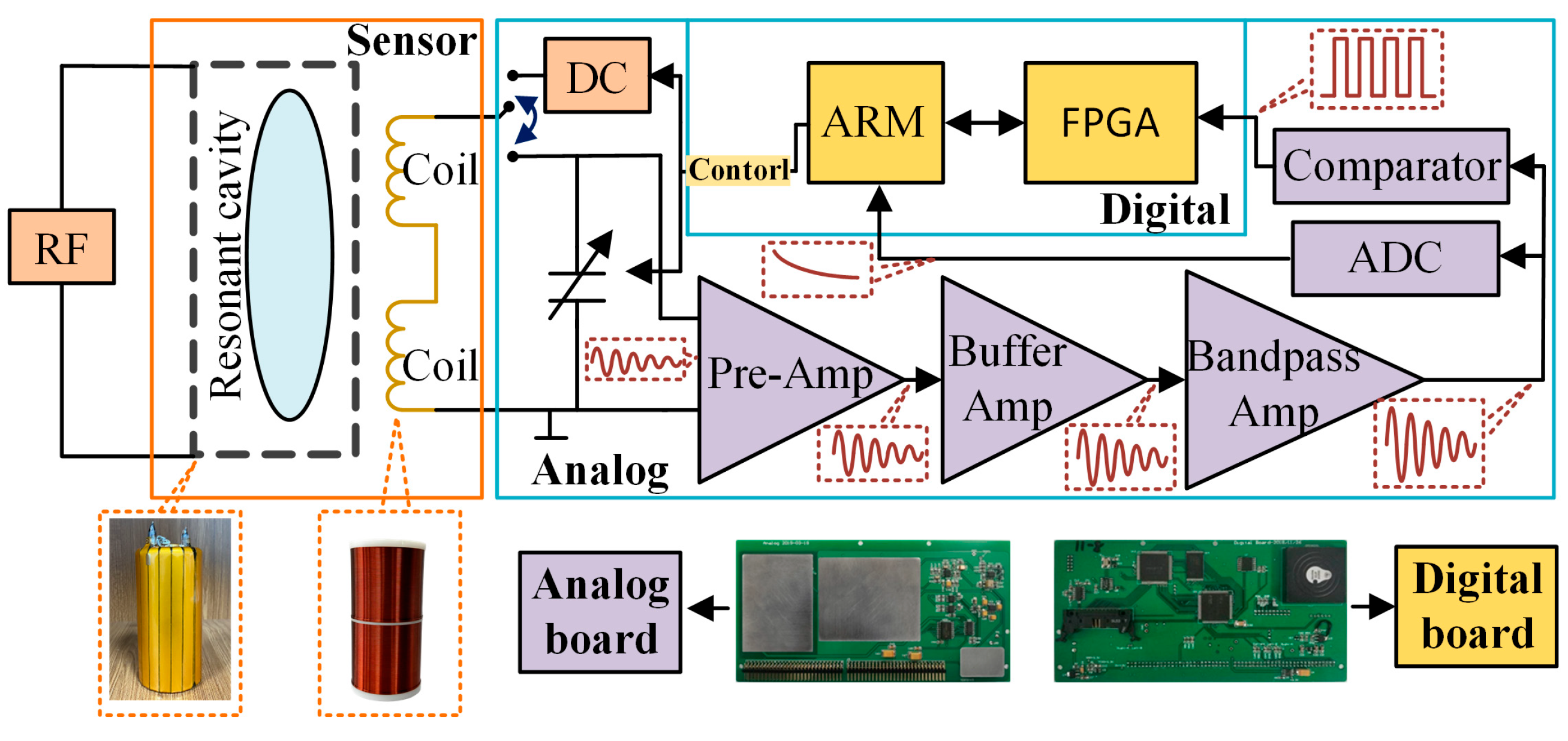
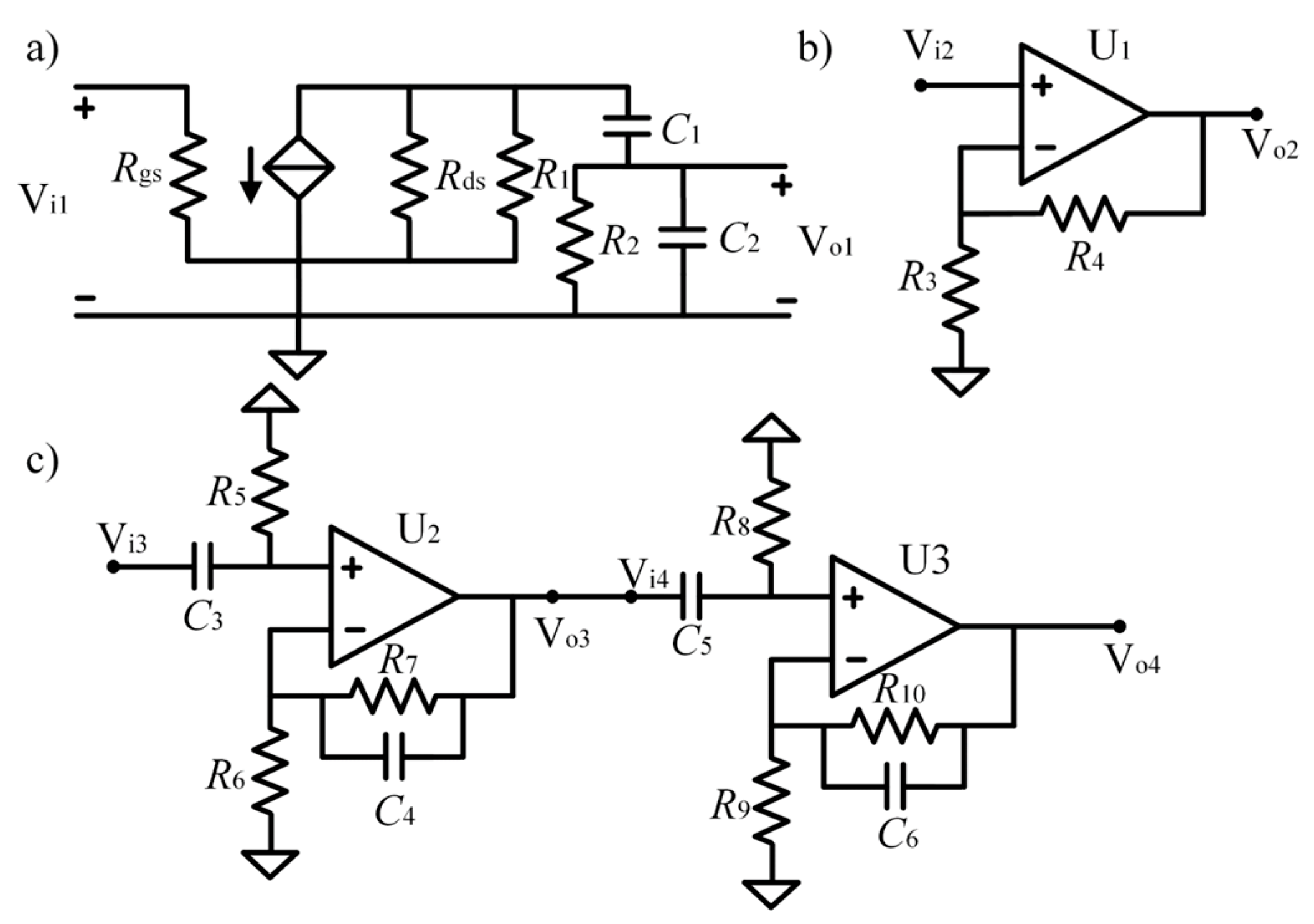
From the above analysis, it can be seen that the LC resonant circuit will affect the noise spectral density, and the signal conditioning circuit of the OVM is used to amplify and filter the signal, and its amplitude-frequency characteristics will also further affect the noise spectral density. In order to establish the comprehensive noise model of the OVM, the transmission characteristics of the signal conditioning circuit will be analyzed in this paper. The signal conditioning circuit of OVMs includes preamplification, buffer amplification, and bandpass filter amplification, as shown in
Figure 4.
The preamplifier used is a low-noise JFET, the equivalent small signal model circuit diagram is shown in
Figure 4a, and the transfer function is
Figure 4.
Signal conditioning circuits. (a) JFET preamplifier circuit small signal model. (b) Buffer amplifier circuit equivalent circuit. (c) Bandpass amplifier circuit equivalent circuit.
Figure 4.
Signal conditioning circuits. (a) JFET preamplifier circuit small signal model. (b) Buffer amplifier circuit equivalent circuit. (c) Bandpass amplifier circuit equivalent circuit.
The buffer amplifier circuit is used to increase the load capacity and reduce the influence of the load on the signal source. The equivalent circuit diagram is shown in
Figure 4b, and its transfer function is
The bandpass filter amplifier is mainly designed to suppress low-frequency noise, such as 50 Hz, and to provide −40 dB/decade attenuation in the high-frequency section to ensure a stable amplitude of the FID signal within the measurement range. The equivalent circuit is shown in
Figure 4c, and the first-stage transfer function is
Similarly, the transfer function of the second-stage circuit is
The transfer function
Hs of the signal conditioning circuit is
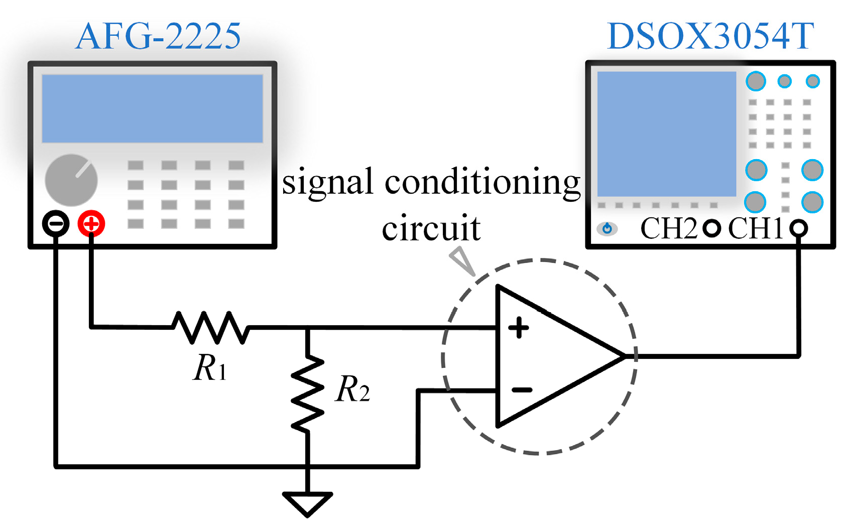
To verify the correctness of the theoretical model, we set up an experimental test platform in the laboratory, using a function generator (GW Instek AFG-2225, New Taipei City, Taiwan) to generate sinusoidal signals in the range of 500–5100 Hz and a high-precision oscilloscope (Keysight DSOX3054T, Santa Rosa, CA, USA) to measure the signals at the output, and the test configuration is shown in
Figure 5. The measured transmission characteristic is shown in
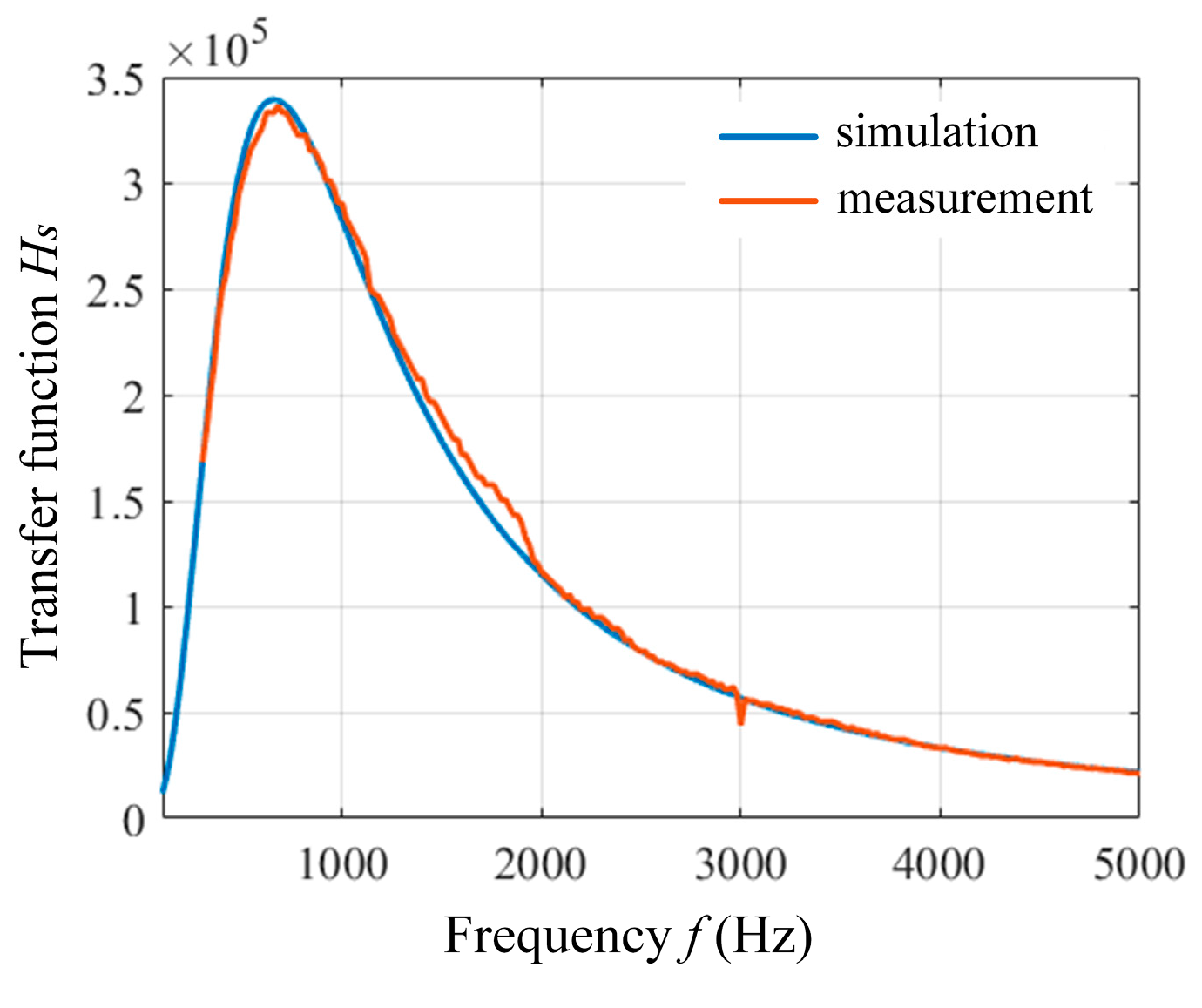
Figure 6 (orange curve). The theoretical calculation of the transfer function of the signal conditioning circuit was performed according to (12)–(16), and the results are shown in
Figure 6 (blue curve). The results show that the theoretical calculation is highly consistent with the measured data, verifying the correctness of the transfer function model. According to the noise analysis results at the amplifier input node INP in the previous section, combined with the transmission characteristics of the signal conditioning circuit, we can establish the total noise model of the OVM, which can be expressed as
where
ee represents the interference of EMI and other noise in the environment, which is random and uncontrollable, and depends only on the external environment.
4. Low-Noise OVM Design
As shown in (17), the output noise of the OVM mainly comes from resistive thermal noise, amplifier voltage noise, and amplifier current noise. In order to complete the design of a magnetometer with high SNR, this paper will further analyze the influence mechanism of each type of noise and discuss the strategy to reduce the output noise. When analyzing the impact of a certain type of noise on system performance, other noise sources will be assumed with reasonable reference values to ensure the pertinence of the analysis.
4.1. Matching Resistance Determination
The quality factor and bandwidth of the LC resonant circuit vary with the matching resistance
R, and different
R values correspond to different thermal noise. In order to determine the optimal
R, an equivalent source impedance
Rs at the input of the amplifier can be written as
In order to optimize the selection of source impedance, we use the noise figure (
NF) to estimate the effect of different source impedances on the noise performance of the system. The
NF is defined as the ratio of the input
SNRin to the output
SNRout, which can be expressed as
where
Po is the output noise power, which is composed of the current noise (
GinRs)
2, voltage noise (
Gen)
2, and source impedance thermal noise (
)
2;
Pi is the noise power at the input, which is mainly contributed by the source impedance thermal noise. Supposing that the bandwidth of the LC resonant circuit is
BW, after substituting each part of the noise, (19) can be further expressed as
Suppose that the coil resistance, inductance, voltage noise, and current noise are 34.2 mH, 18.2 Ω, 1.4 nV/
and 0.1 pA/
[
26], respectively, we calculate the effect of the source impedance
Rs on the noise figure
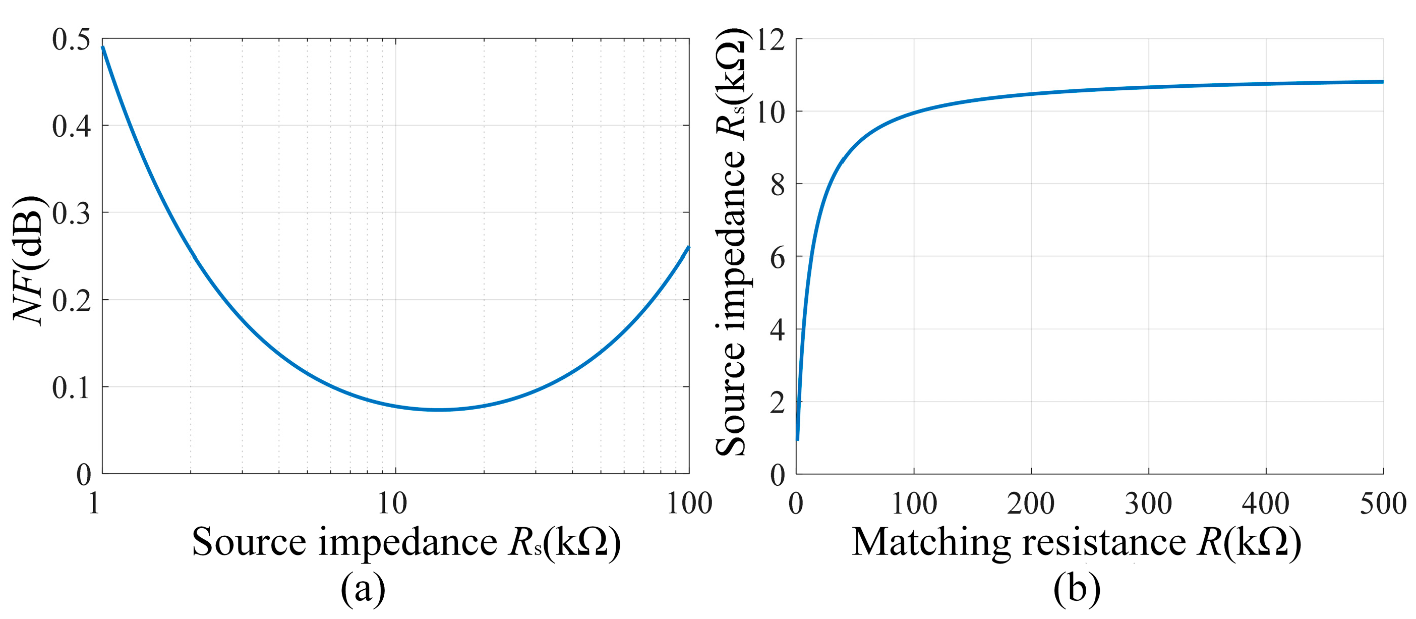
NF at 2.1 kHz according to (20), and the result is shown in
Figure 7a. The results show that there exists a minimum value of the noise figure
NF when the source impedance
Rs is varied in the range of 1~100 kΩ, and the minimum value of
NF occurs when
Rs is between 10 kΩ and 20 kΩ.
In addition, we calculate the variation of source impedance
Rs with matching resistance according to (19). It can be seen from
Figure 7b that the source impedance
Rs remains unchanged when the matching resistance is larger than 100 kΩ. Given that the minimum value of the
NF corresponds to
Rs of about 10~20 kΩ and considering that a larger matching resistance also means a higher quality factor
Q, which helps to improve the resonance performance, the matching resistance is finally chosen to be 100 kΩ.
Figure 7.
(a) The source impedance Rs vs. matching resistance R. (b) Noise figure NF vs. source impedance Rs.
Figure 7.
(a) The source impedance Rs vs. matching resistance R. (b) Noise figure NF vs. source impedance Rs.
4.2. Parameter Analysis of Sensor Audio Coil and Preamplifier
The noise of the audio coil depends on its resistance, which is determined by both the number of turns and the wire diameter. When the number of turns is small and the wire diameter is large, the resistance is low, but the signal amplitude also decreases. To achieve a balance between signal strength and noise control, it is necessary to optimize the design of the coil, including the number of turns and wire diameter. For simplicity, we suppose that the wire diameter is constant and the influence of the number of turns on the SNR will be investigated to determine the optimal number of turns.
The relationship between the resistance value and the number of turns of the coil is
where
is the coil resistivity, and
d is the coil wire diameter. When the coil frame is determined, the inductance of the finite field multi-layer hollow coil is [
27]
where
kn is the fixed coefficient. According to (3), the initial amplitude of the FID signal can be expressed by
n as
where
E0 is the constant product in (3). The equivalent value of the noise at the output of the system can be calculated by the following equation
where
f1 and
f2 are the lower and upper cutoff frequencies of the bandpass filter, respectively. The SNR of the OVM output is
where
f0 is the LC circuit resonant frequency, and
Hs(
f0) is the gain of the signal conditioning circuit transfer function
Hs at the frequency
f0. According to (17), (21)–(25), and assuming that the voltage noise of the preamplifier is 1 nV/
and the current noise is 0.1 pA/
, the effect of the number of turns
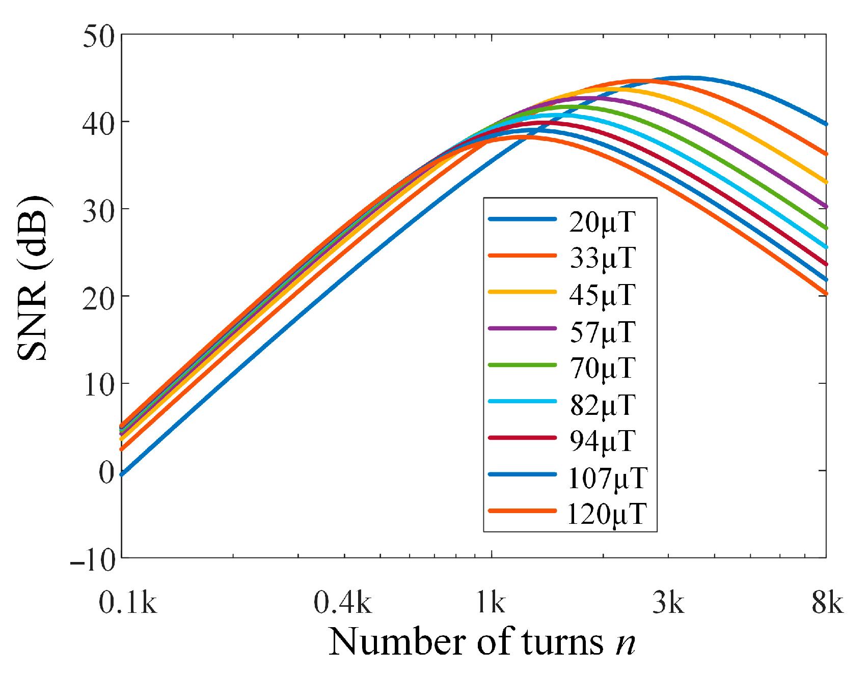
n on the SNR at different resonant frequencies is calculated, and the results are shown in
Figure 8.
From the results in
Figure 8, it can be seen that there is an optimal number of coil turns within the measurement range of 20 μT (851 Hz)–120 μT (5109 Hz). When the number of turns is around 1500, the SNR in the range of 20 μT–120 μT is averaged to the maximum value, and the difference in SNR between different field strengths is small. Insufficient turns result in a lower amplitude of the Larmor signal, leading to a poor overall SNR. However, excessive turns lead to a decrease in SNR and enlarge the difference in SNR. Moreover, increasing the number of turns increases the volume of the sensor, reducing the portability of the system. Comprehensively, we selected 1400 turns of enameled copper wire with a wire diameter of 0.54 mm, and the resistance and inductance are 22.5 Ω and 33.5 mH, respectively.
According to (9) and (24), we calculated the impact of the voltage and current noise of JFET on the root mean square (rms) value of the system output noise. The calculation results show that both the voltage noise and current noise output by the system increase linearly with the increase of JFET’s own noise, and this indicates that the noise performance of the device itself has a significant impact on the system output noise. In order to reduce system output noise, JFET devices with low voltage noise and low current noise should be prioritized, and these two parts of noise should not be higher than the coil resistance thermal noise. Based on this analysis, we select 2N6550 as the preamplifier, whose voltage noise is 1.4 nV/ and current noise is 0.1 pA/.
Finally, the optimized low-noise design parameters are listed in
Table 1. Combining (17) and the parameters in
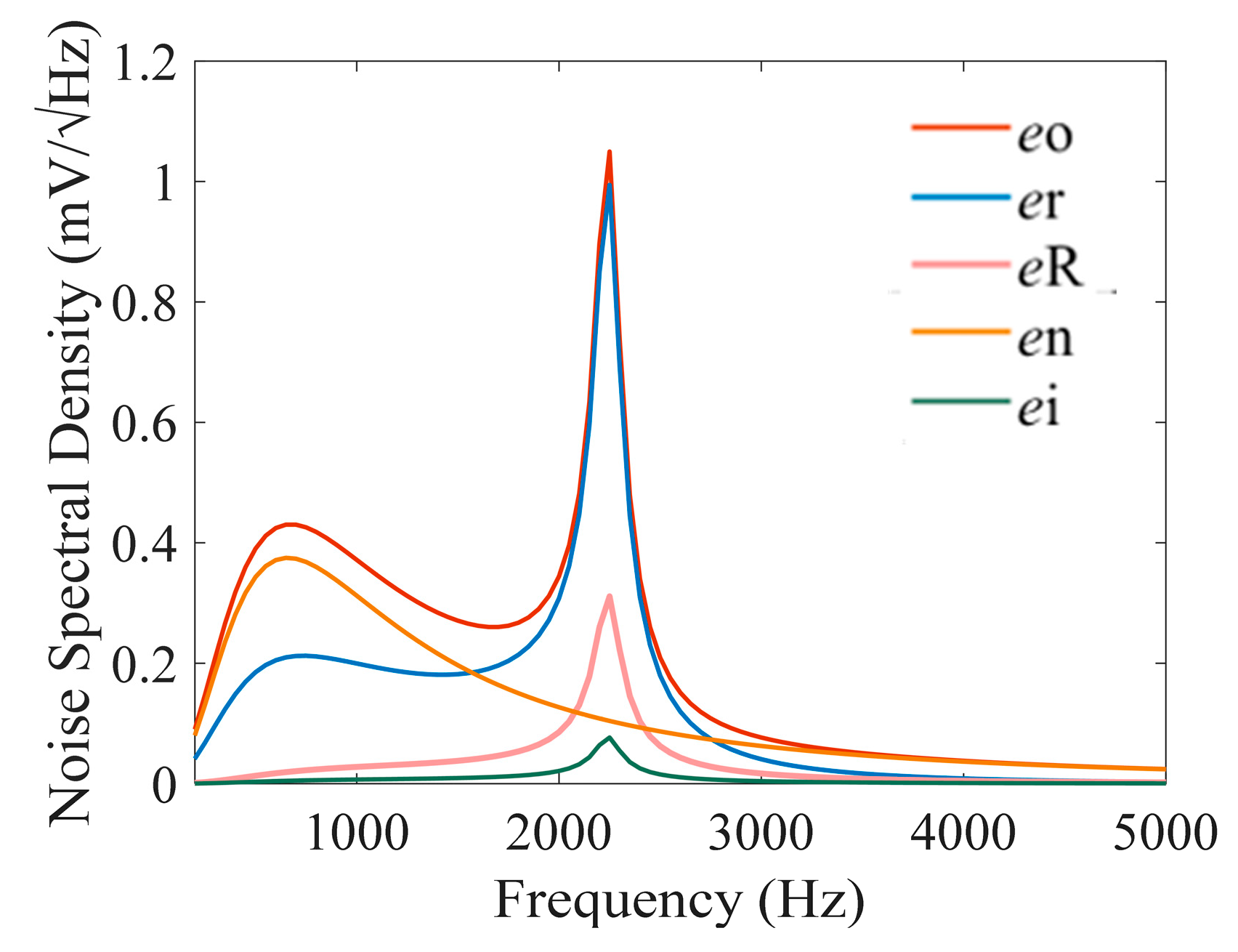
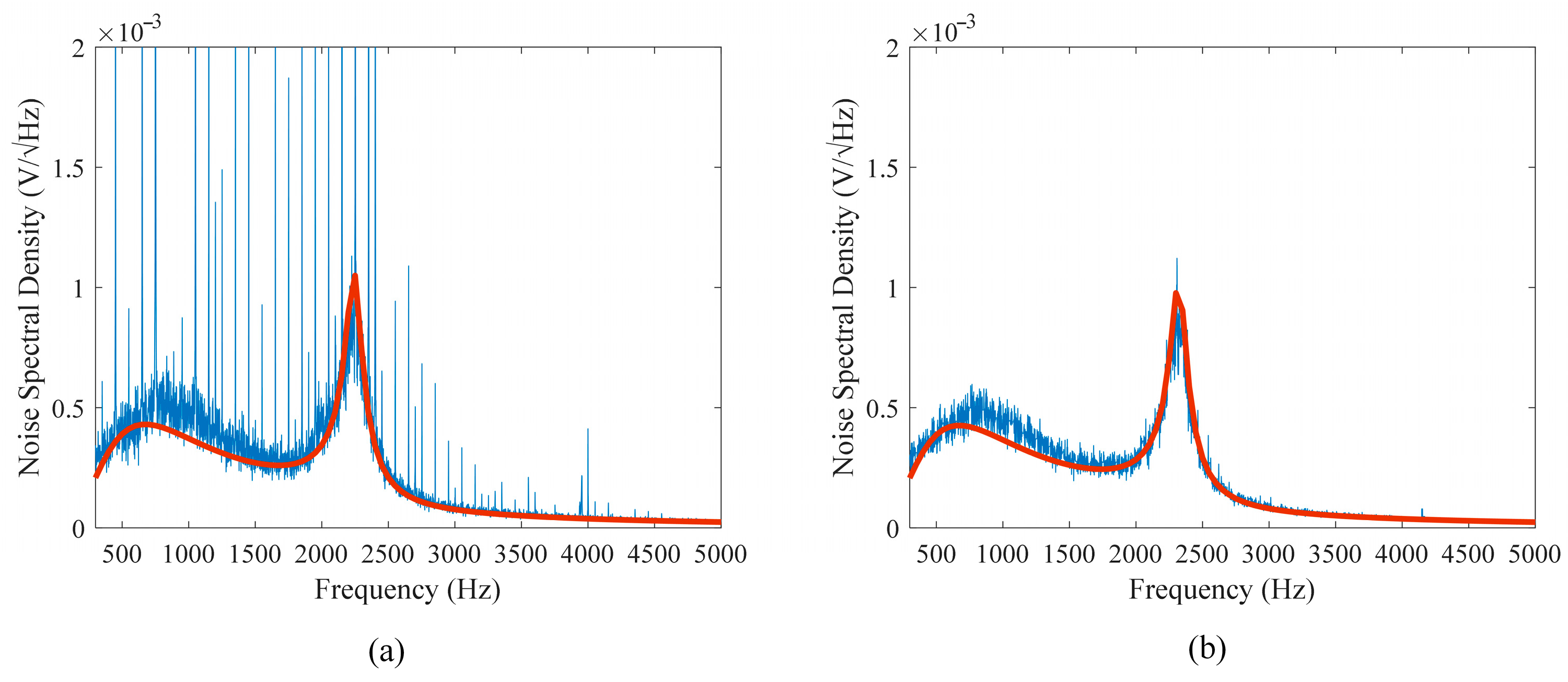
Table 1, the calculated equivalent noise spectral density is shown in
Figure 9. Results indicate that noise at resonant frequency is mainly contributed by the coil resistance thermal noise, whose noise density can reach 1.0 mV/
; Outside the resonant frequency band, the main source of the noise is the voltage noise, whose maximum noise density can reach 0.4 mV/
.
Figure 9.
Estimated noise contributions after the signal conditioning circuit.
Figure 9.
Estimated noise contributions after the signal conditioning circuit.
Table 1.
Optimized vs. unoptimized audio coil and preamplifier electrical parameters.
Table 1.
Optimized vs. unoptimized audio coil and preamplifier electrical parameters.
| Parameter | Optimized Value | Unoptimized Value |
|---|
| Audio coil resistance r | 22.5 Ω | 28 Ω |
| Audio coil inductance L | 33.5 mH | 34 mH |
| Matched resistance R | 100 kΩ | 50 kΩ |
| Resonance frequency f0 | 2.3 kHz | 2.3 kHz |
| Gain of preamplifier G | 32 | 32 |
| Preamplifier voltage noise en | | |
| Preamplifier current noise in | | |
According to (24) and the parameters in
Table 1, the rms of different types of noise is calculated and shown in
Table 2. The results show that the total noise output of the optimized system is 23.93 mV, compared to 28.6 mV for the unoptimized parameters, representing a theoretical noise reduction of 4.7 mV. The main noise sources are the thermal noise of the coil resistor (17.62 mV) and the voltage noise of the preamplifier (15.51 mV). Compared to the voltage noise and thermal noise of coil resistance, the contribution of the current noise and the thermal noise of the matching resistor is negligible.
6. Conclusions
An equivalent circuit model of noise is proposed to investigate the intrinsic noise characteristics of the OVM. Calculated results show that the intrinsic noise of the OVM mainly comes from the resistance thermal noise of the sensor audio coil and the voltage noise of the JFET preamplifier. The amplitude-frequency characteristics of the circuit significantly influence the noise bandwidth, thus affecting the final spectral characteristics of the noise.
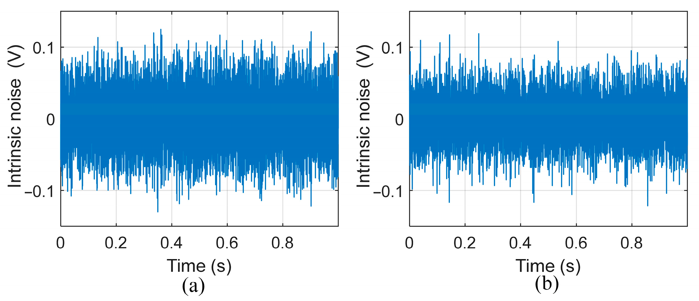
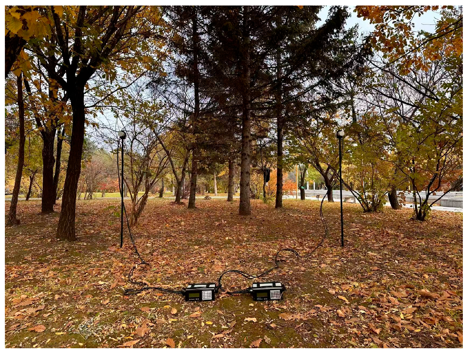
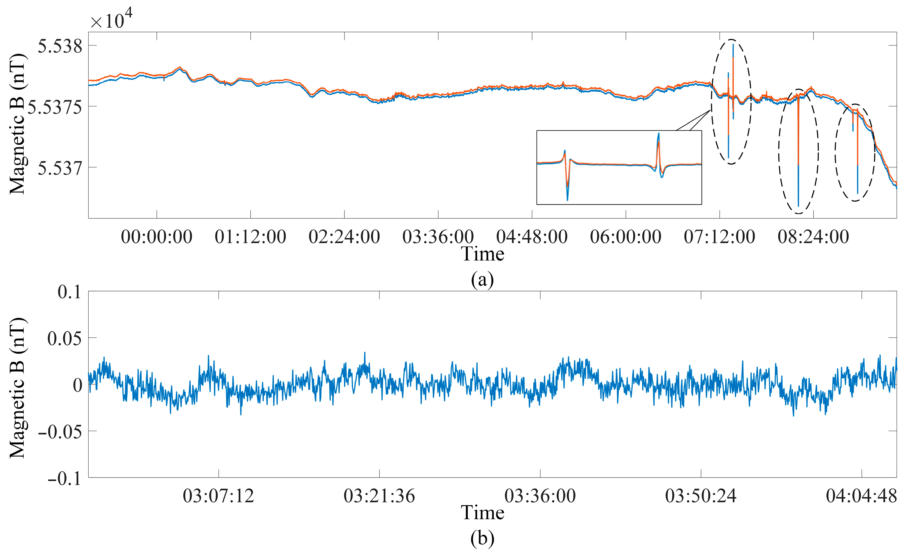
The parameters of the OVM sensor, matching resistor, and preamplifier were optimized based on the noise model proposed in this article. The intrinsic noise of the system is measured in the natural environment, and the results show that the measured rms of the system noise is 26.7 mV, representing a 12% deviation from the theoretical value of 23.9 mV. Sensitivity is estimated in the natural magnetic field by using two synchronized instruments, and the sensitivity of the OVM is 0.0079 nT at 3 s. This sensitivity is significantly lower than the usual 0.01 nT at the same cycling time, indicating the effectiveness of this noise model in suppressing inherent noise. Compared to the method that improves SNR through signal processing algorithms, this method is simpler and more efficient, making it more suitable for real-time measurement.
The noise model proposed in this paper is not only suitable for low-noise OVM design, but also for other instruments with sensor coils.
