Article

High-Density Arrayed Spectrometer with Microlens Array Grating for Multi-Channel Parallel Spectral Analysis

Tsinghua Shenzhen International Graduate School, Tsinghua University, Shenzhen 518055, China
*
Author to whom correspondence should be addressed.
Sensors 2025, 25(15), 4833; https://doi.org/10.3390/s25154833
Submission received: 30 June 2025 / Revised: 31 July 2025 / Accepted: 2 August 2025 / Published: 6 August 2025

Abstract

To enable multi-channel parallel spectral analysis in array-based devices such as micro-light-emitting diodes (Micro-LEDs) and line-scan spectral confocal systems, the development of compact array spectrometers has become increasingly important. In this work, a novel spectrometer architecture based on a microlens array grating (MLAG) is proposed, which addresses the major limitations of conventional spectrometers, including limited parallel detection capability, bulky structures, and insufficient spatial resolution. By integrating dispersion and focusing within a monolithic device, the system enables simultaneous acquisition across more than 2000 parallel channels within a 10 mm × 10 mm unit consisting of an f = 4 mm microlens and a 600 lines/mm blazed grating. Optimized microlens and aperture alignment allows for flexible control of the divergence angle of the incident light, and the system theoretically achieves nanometer-scale spectral resolution across a 380–780 nm wavelength range, with inter-channel measurement deviation below 1.25%. Experimental results demonstrate that this spectrometer system can theoretically support up to 2070 independently addressable subunits. At a wavelength of 638 nm, the coefficient of variation (CV) of spot spacing among array elements is as low as 1.11%, indicating high uniformity. The spectral repeatability precision is better than 1.0 nm, and after image enhancement, the standard deviation of the diffracted light shift is reduced to just 0.26 nm. The practical spectral resolution achieved is as fine as 3.0 nm. This platform supports wafer-level spectral screening of high-density Micro-LEDs, offering a practical hardware solution for high-precision industrial inline sorting, such as Micro-LED defect inspection.

1. Introduction

As a core instrument for characterizing the wavelength–intensity relationship, the spectrometer plays a crucial role in a wide range of applications, including spectral analysis of light-emitting devices, confocal microscopy, multi-component atmospheric pollutant monitoring, ophthalmic diagnostics, and climate observation [1,2,3,4,5]. Taking spectral confocal technology as an example, this high-precision, non-contact optical measurement technique leverages the wavelength-dependent focal response of a broadband light source along the axial direction [6,7,8,9]. By employing spectroscopic analysis, it decodes displacement [10,11,12,13,14,15,16,17,18], film thickness [19,20,21,22,23,24], roundness [25,26,27], and surface reflectivity [28,29,30] information that is encoded in the wavelength of the reflected light. This approach demonstrates excellent resolution and accuracy, even though many traditional and emerging techniques are also available for obtaining such measurement information [31,32,33].
To meet the demands of these diverse applications, spectrometer technology has evolved toward broader spectral coverage, miniaturization, and higher levels of integration in recent years [34,35,36,37,38]. On the one hand, advances in the fabrication of concave gratings with large groove constants and high curvature have enabled the development of compact spectrometers with broad spectral coverage [39,40,41,42,43]. Although approaches based on metasurfaces, integrated photonics, and compressive sensing have enabled compact and broadband spectrometer designs, these methods often face challenges such as complex fabrication, limited throughput, or the need for intensive computational reconstruction, which may impede their use in high-density parallel detection [3,5]. On the other hand, the rapid development of integrated photonics and multi-emitter sources—such as vertical-cavity surface-emitting laser (VCSEL) arrays, Micro-LED arrays, and spectral confocal line-scan systems—has led to a significant increase in the demand for multi-channel parallel processing aimed at planar scanning and even three-dimensional information acquisition. These trends impose higher requirements on both the measurement efficiency and data processing capabilities of modern spectrometers [44,45,46,47]. In response, researchers have proposed new array-based spectrometer architectures that enable high-throughput spectral analysis through multi-channel parallel processing [48,49,50,51,52,53].
Commercial multi-channel spectrometers typically adopt stacked architectures composed of multiple single-channel modules. Representative examples include the Ocean Optics eight-channel spectrometer (180–1100 nm, 0.1 nm resolution, 7 kg) and the HORIBA 96-channel spectrometer (360–780 nm, <3.5 nm resolution) [54,55]. These conventional designs are constrained by their bulky size, heavy weight, and limited channel scalability, making them ill-suited for high-density and highly integrated applications in industrial manufacturing. To overcome these limitations, recent efforts have focused on integrating dispersive and focusing functions within miniaturized optical components [56,57,58,59]. For example, Traut et al. [60] employed photolithographic holography to fabricate microlens–grating composite structures (resolution > 10 nm); Hirano et al. [61] constructed a blazed grating–microlens array system via physical vapor deposition and electron beam lithography; and Shi et al. [62] applied thermal reflow self-assembly to realize microlens array gratings with a resolution of 6.9 nm. However, these approaches often encounter significant technical challenges, such as the need for cleanroom conditions and material shrinkage during polymer curing. In parallel, miniature spectrometers using Fresnel lenses have been developed to further reduce system footprint and enhance compactness [63,64,65]. While such designs can achieve high spectral resolution (down to 0.2 nm), they face scalability issues when increasing the number of parallel detection channels.
Several recent strategies have been proposed to enable multi-channel parallel spectral analysis. For instance, Shan et al. [66] developed a microlens array–grating (MLAG) technique using soft lithography to integrate multiple spectral units, achieving a 220 μm channel pitch and sub-pixel spot center repeatability, thus demonstrating strong potential for high-density parallel detection. However, the system still relies on external optics to adjust divergence angles. Fathy et al. [67] proposed a multi-interferometer approach based on micro-electro-mechanical systems (MEMS) that improves spectral resolution through multipath interference, achieving up to a threefold enhancement, though its performance is limited by the thermal stability of MEMS actuators. Hybrid micro-optical systems have also been explored to bridge performance gaps. For example, Hao et al. [68] introduced a multi-aperture snapshot imaging spectrometer employing tilted linear variable filters (LVFs) and a microlens array, realizing an 11 × 6 spectral channel matrix, albeit with spectral distortion at large apertures. Similarly, Chen et al. [69] proposed an infrared array spectrometer achieving high resolution at the expense of optical throughput (i.e., photon efficiency). Collectively, these approaches underscore an enduring trade-off in multiplexed spectral sensing: scalability versus performance.
To address this challenge, we propose a novel spectrometer architecture specifically designed for multi-channel parallel spectral detection. The core element of the system is a double-sided integrated microlens array grating (MLAG) that simultaneously performs dispersion and focusing. This is complemented by a dual-microlens aperture assembly that enables flexible adjustment of the divergence angle of the incident light. A CMOS sensor serves as the detection module, while spectral data are processed by a higher-level computing system to enable multispectral co-analysis. Building upon previous work [66], this study further advances the overall optical design, experimentally validates the performance of the array-based spectrometer, and proposes an image enhancement algorithm to improve resolution. The results show that the fabricated device comprises up to 2070 spectral units, exhibiting high uniformity and consistent dispersion characteristics. Single-channel spectral measurements confirm effective dispersion, with spectral resolution at the nanometer level and repeatability better than 1 nm.

2. Structure and Operating Principle of Multi-Channel Spectrometers

2.1. Structural Composition of Multi-Channel Spectrometers

Figure 1 illustrates the structural schematic of the proposed multi-array, multi-channel spectrometer system. The system is designed for testing array-based light sources, such as Micro-LED arrays and spectral confocal line-scan probes. The light source is initially focused and its sub-source size reduced through a microlens array, allowing for efficient coupling into the corresponding channels of an optical fiber array to form an arrayed light source signal. This arrayed light then passes through a scattering angle adjustment module—comprising a microlens array, an aperture, and another microlens array—which flexibly adjusts the output angles in accordance with the diameter of the MLAG subunits. As a result, an arrayed light source with a defined scattering angle is produced. Each sub-source subsequently enters its corresponding MLAG unit, where it undergoes further focusing and dispersion. The resulting spectrally dispersed light is imaged onto a CMOS sensor, enabling the acquisition of spectral signals. The spectral data from all sub-sources are collected simultaneously, thereby achieving multi-channel parallel spectral analysis.

2.2. Operating Principle of Microlens Array Grating Spectrometers

The fundamental working principle of a dispersive spectrometer lies in spectral dispersion—that is, separating incident light into its constituent wavelengths for analytical purposes. Such systems typically comprise three core components: an entrance slit, a dispersive element, and a detector. The entrance slit spatially confines the incoming light, ensuring well-defined beam boundaries prior to interaction with the dispersive element.
At the heart of multi-channel spectrometer functionality is the MLAG. Figure 1 illustrates the structural composition of an MLAG subunit. Each subunit consists of a microlens for focusing incident light and a diffraction grating for dispersing the focused beam into its spectral components. Due to the small aperture of the microlenses, only a limited number of grating lines are illuminated, which in turn affects the spectrometer’s resolution. To address this, a blazed grating with a blaze angle of 8°37′ and a blaze wavelength of 500 nm was employed in the experiment to enhance the intensity of the diffracted light on one side. Additionally, image processing techniques were applied to further improve the resolution.
During operation, incident light enters the MLAG system and first interacts with the microlens array. The microlenses focus the light into discrete spots, ensuring that each optical path is well-defined and spatially confined. These focused beams then pass through a diffraction grating with period d, where they are diffracted at angles that depend on their wavelengths. This diffraction process spatially separates the light into its spectral components, with each wavelength deflected at a characteristic angle as defined by Equation (1).
d sin α ± d sin θ = m λ , m = 0 , ± 1 , ± 2
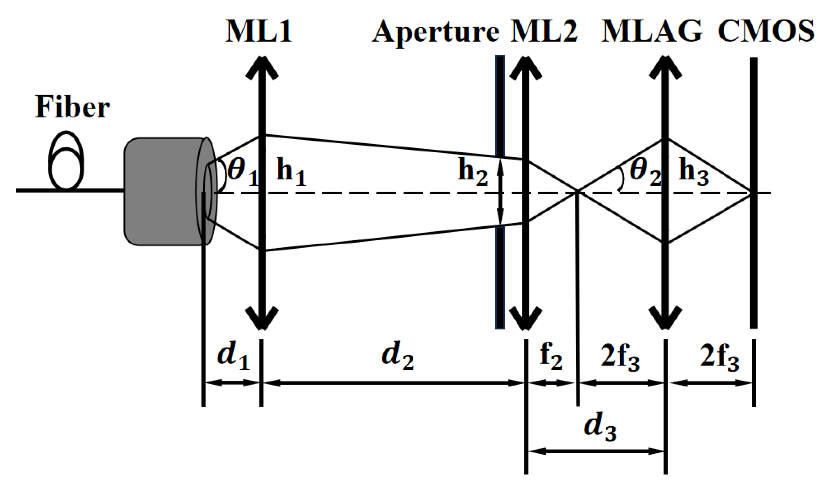
In addition, another key component of the array-based spectrometer is the incident light divergence angle adjustment assembly , which consists of a pair of microlens arrays and a pinhole aperture. Figure 2 illustrates the optical path for implementing a single-channel spectrometer. The laser is emitted through an optical fiber port, with an output beam diameter h 1 = 105 μm.
The primary function of the two microlens arrays is to adjust the divergence angle of light incident on MLAG subunits, thereby ensuring compatibility with MLAG sub-arrays of arbitrary sizes. Specifically, ML1 serves to collimate the light, which emerges from the optical fiber with a certain divergence angle, while ML2 focuses the collimated beam. By adjusting the distances between the light source and the two microlens arrays, the divergence angle of light incident on each MLAG subunit can be finely tuned. To achieve optimal image quality and prevent crosstalk between neighboring MLAG focal spots, the incident divergence angle prior to entering the MLAG should satisfy the following condition:
θ 2 arctan h 3 2 f 3
Here, h 3 denotes the width of the MLAG subunit, and f 2 represents the focal length of the MLAG lens element.
Similarly, the pinhole aperture serves to adjust the size of the optical source image to match the lens aperture of the MLAG subunits. If the focal spot is too large, it reduces the number of available channels, degrades spectral resolution, and increases the likelihood of channel crosstalk. Conversely, if the spot is too small, the light utilization efficiency decreases, and measurement repeatability is compromised.
It is important to note that the parameter values used in this study represent only one feasible configuration. In practice, these parameters can be flexibly modified and recombined as needed. The proposed divergence-angle adjustment module can be readily adapted to MLAG elements with varying sub-lens diameters, thus enabling a configurable multi-channel array spectrometer compatible with a wide range of array-type light sources.

3. Experimental Validation of the Array-Based Spectrometer

3.1. Construction and Calibration of the Array Light Source System

As illustrated in Figure 3a, the spectrometer system consists of a laser source, a divergence-angle adjustment module (comprising a microlens–aperture–microlens assembly), a spectral dispersion module based on the MLAG, and a CMOS detector for signal acquisition. In the experiment, the laser provides light at different wavelengths to evaluate the functional performance and uniformity of the array. The laser is coupled into the system via an optical fiber with a core diameter of 105 μm and a numerical aperture (NA) of 0.22. The light then passes through the MLA1–aperture–MLA2 module and subsequently illuminates the MLAG. The CMOS sensor captures the resulting far-field pattern, enabling analysis of focusing behavior and spot uniformity.
After assembling the microlens grating array spectrometer, it is necessary to calibrate the correspondence between CMOS pixel indices and the associated wavelengths. This is achieved by fitting a calibration curve based on measured data. In general, increasing the number of data points or using higher-order polynomials improves the fitting accuracy. However, when the curve exhibits only slight variation, higher-order fitting may offer negligible improvement in detection accuracy while incurring greater computational cost. Therefore, a trade-off must be made between accuracy and computational efficiency. In this study, three wavelengths are selected for calibration, and a second-order polynomial fitting is applied, as expressed in Equation (3):
L = a 0 p 2 + a 1 p + a 2
Here, L denotes the actual wavelength, and p represents the pixel displacement between the first-order and zeroth-order diffraction spots (i.e., the center-to-center distance between the spots on the CMOS sensor). By differentiating Equation (3), the spectral resolution corresponding to the width of a single pixel can be obtained:
L = 2 a 0 p + a 1
As shown in Equation (4), the focal spot position on the CMOS sensor is directly related to the wavelength of the incident light and is independent of other spatial variables. As a result, the spectral width associated with each pixel is non-uniform across the sensor.

3.2. Subunit Uniformity Test

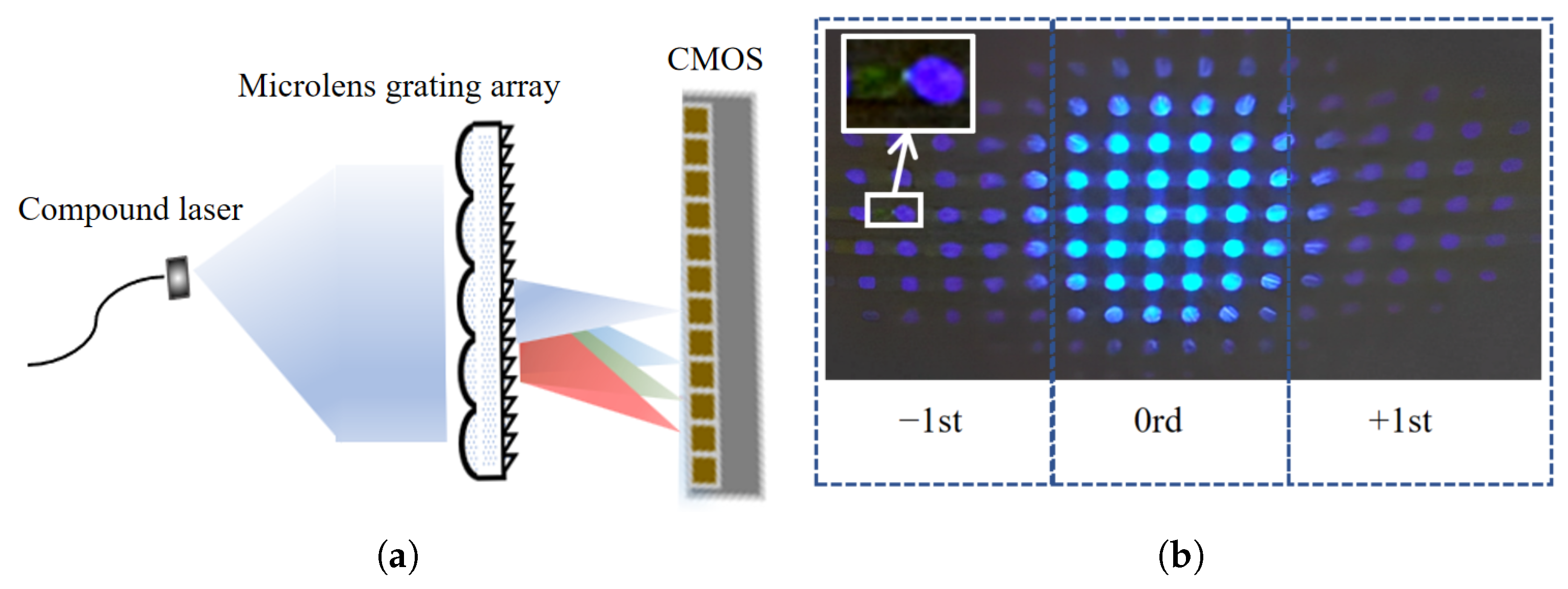
Since the core component of the array-based spectrometer is the MLAG, its fundamental functionality and uniformity were first verified to evaluate the consistency across individual spectrometer subunits. As shown in Figure 4a, a composite blue-green laser source was coupled into the system via an optical fiber. After collimation by a lens, the parallel beam was directed onto the MLAG surface. The resulting imaging, shown in Figure 4b, demonstrates that the parallel beam is focused on multiple sub-spots distributed across different channels with no visible crosstalk and relatively uniform brightness in the central region. On either side of the central focus, distinct ±1st-order diffraction spots are observed, indicating effective wavelength separation between the blue and green components. These results confirm the MLAG’s strong focusing and dispersive capabilities, validating its role as the core element of the spectrometer.
To quantitatively assess subunit uniformity, a single-point laser source was expanded into a regular grid of equally spaced laser spots by the MLAG, forming a uniform array pattern. The centroid position of each spot was calculated to determine pixel locations, and the distances between adjacent centroids were measured. By translating the MLAG along the x- and y-axes, the imaging uniformity of the entire device was assessed. Table 1 presents the distances between 0th-order focus and its neighboring spots in the x-direction (right) and y-direction (down) for randomly selected subunits at different positions. These values were used to evaluate the spatial uniformity of the microlens array. The coefficient of variation (CV), defined as the standard deviation divided by the mean, was used as a measure of uniformity—lower CV values indicating better consistency. The measured CV values were 1.25% in the x-direction and 1.11% in the y-direction, suggesting slightly better uniformity along the y-axis.

3.3. Spectrometer Channel Performance Testing

3.3.1. Single-Unit Testing in the Array-Based Spectrometer

To clearly illustrate the system’s performance, we first present the spectral results of a single spectrometer subunit, which can be generalized to the array level by replacing individual components with full arrays. The test system, illustrated in Figure 3b, employs a three-wavelength composite laser source (660 nm/520 nm/450 nm). The laser is delivered through an optical fiber with a 105 μm core diameter. The first microlens array (MLA1) consists of subunits with a side length of 125 μm and a focal length of 0.4 mm. Given physical constraints on the fixed components, MLA1 serves to collimate the light beam. A pinhole aperture with a 100 μm diameter limits the entrance pupil size. The collimated beam is then focused by MLA2 (subunit size: 300 μm, focal length: 5 mm), which is carefully positioned relative to the MLAG to achieve optimal focusing. After passing through the MLAG, light at each wavelength is diffracted and focused at different positions on the image plane.
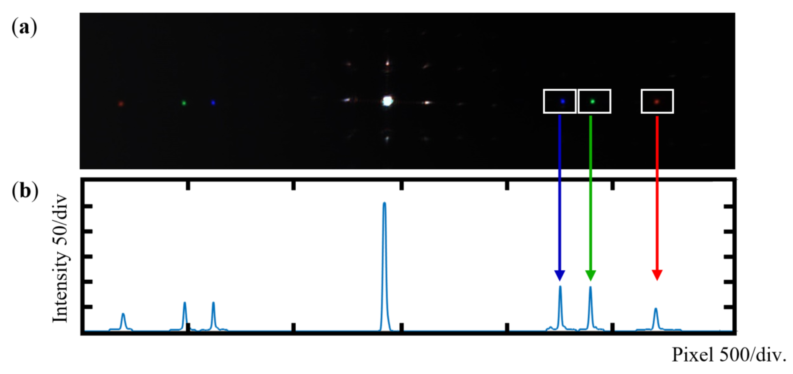
When the beam is aligned perpendicularly to a specific MLAG microlens subunit, the spectrometer parameters are fixed. The three wavelengths are sequentially focused onto the CMOS detector, where 0th-order and ±1st-order diffraction spots are simultaneously captured. As shown in Figure 5a, only the +1st-order diffraction pattern is displayed due to its symmetry with the −1st order; unless otherwise noted, the +1st-order signal is used for analysis throughout this work. Since raw spectral data may be affected by stray light, a simple filtering step is applied to remove background noise. The intensity distribution is then extracted, and the diffraction spot position is determined using a centroid-based method, as illustrated in Figure 5b.
To evaluate the performance across multiple channels, a 5 × 5 array of microlens subunits was tested, yielding 25 sets of raw data. Based on the symmetry of ±1st-order diffraction, 23 valid datasets were retained for analysis. The directly computed 3σ positional deviation across the focal spots was found to be in the order of several hundred pixels.

3.3.2. Offset Correction

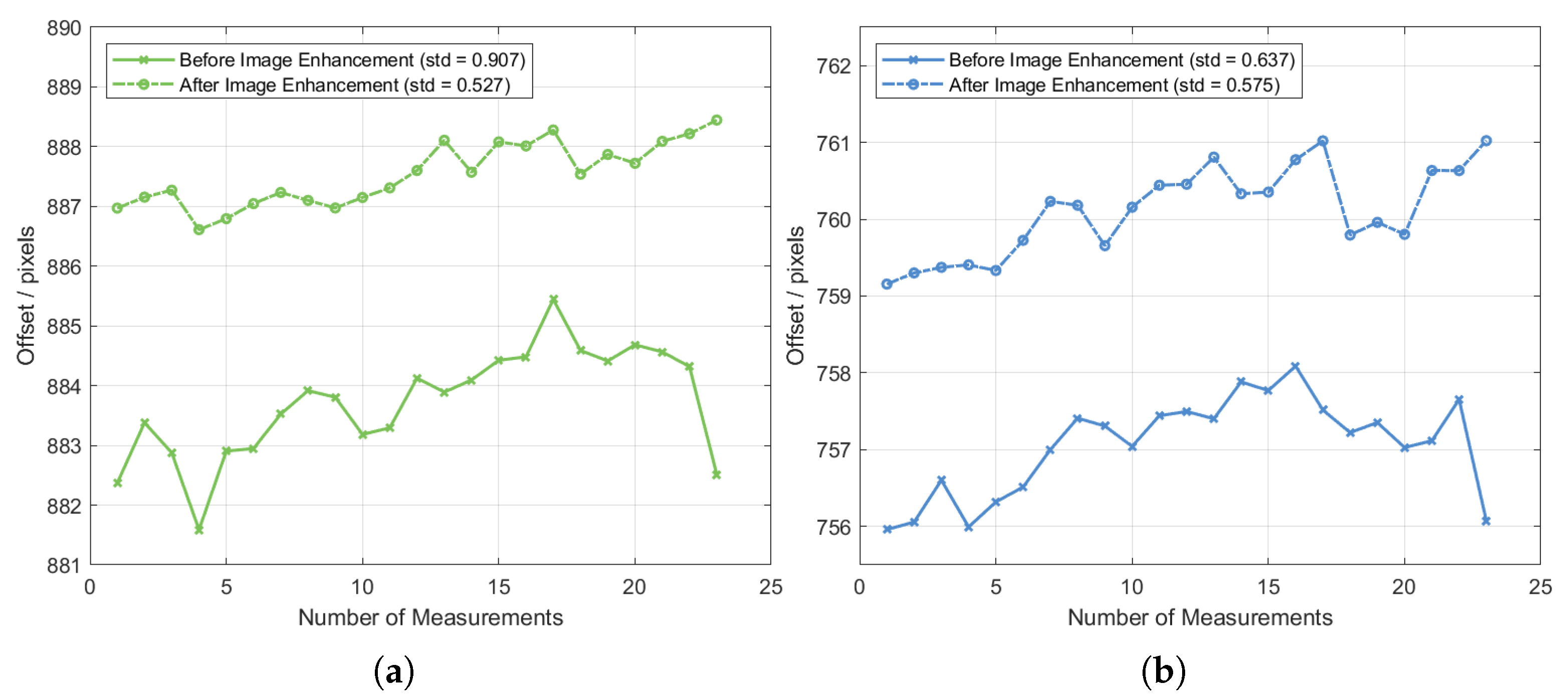
Due to the movement of the microlens array grating relative to the camera during the experiment, the distance between the imaging plane and the grating also changed, resulting in a variation in the overall image size. The solid lines in Figure 6 present the original measurement data arranged in the order in which the experiments were conducted. It can be observed that, as the experiment progresses, the diffraction shifts corresponding to each wavelength increase simultaneously, indicating that the images captured on the CMOS sensor have undergone a consistent scaling in size.
To compensate for this variation, all images were rescaled. The average displacement of the +1st-order red diffraction spot (660 nm) was selected as a reference, and each image was scaled so that the red +1st-order spot displacement was normalized to 1161.8 pixels. After normalization, the pixel center distances for the 520 nm and 450 nm diffraction spots were calculated. As shown by the dashed lines in Figure 6, this correction effectively reduced deviation across images. The mean pixel center distance for the 520 nm diffraction spot was measured to be 887.0 px, with a repeatability (3σ) of 2.72 px. For the 450 nm diffraction spot, the mean pixel center distance was 759.9 px, with a repeatability (3σ) of 1.91 px.
According to the calibration method described in Section 3.1, the fitted parameters obtained after calibration are a 0 = 0.000699 , a 1 = 1.138406 , and a 2 = 106.074939 . Based on these parameters, the spectral widths corresponding to the pixel positions at different test wavelengths are calculated as follows: 0.49 nm at 660 nm, 0.54 nm at 520 nm, and 0.57 nm at 450 nm. The standard deviations (σ) of the pixel center distances for the 520 nm and 450 nm laser sources are 0.45 nm and 0.38 nm, respectively.

3.3.3. Spot Image Enhancement Processing

In the experiment, the outer regions of the diffraction spots exhibited low brightness and were susceptible to background noise, leading to a low signal-to-noise ratio. Moreover, the spots were not perfectly circular. To improve spot localization accuracy, an image enhancement algorithm was applied to suppress the brightness of the outer regions and emphasize the high-energy spot centers for centroid detection. After enhancement, the effective spot size was reduced, and centroid positions were recalculated and rescaled. The revised pixel center distances for the +1st-order diffraction spots of different wavelengths are shown in Figure 7. The standard deviations of the enhanced 520 nm and 450 nm spots were 0.53 px and 0.58 px, corresponding to spectral widths of 0.26 nm and 0.35 nm, respectively.
It should be noted that this error includes not only the localization uncertainty of the 520 nm and 450 nm spots but also the localization error of the 660 nm reference spot, since all measurements were normalized assuming its position was accurate. In scenarios where the relative position between the MLAG and CMOS sensor is fixed, the achievable precision of the system can be further improved.
The image enhancement procedure is as follows:
1.
Contrast enhancement for each spot and its local background using linear mapping:
y = 255 · x m i n m a x m i n
where min and max denote the minimum and maximum brightness in the selected region. The result is shown in Figure 8b.
2.
Nonlinear filtering of brightness using:
y = 1 1 + e k ( x c )
where k and c are filter parameters. For k = 20 and c = 0.95, the enhanced image is shown in Figure 8c.
3.
Thresholding to remove low-brightness pixels. The filtered result is shown in Figure 8d.
The choice of filtering parameters also impacts the measured standard deviation of diffraction spot positions, as shown in Table 2. Increasing suppression of peripheral brightness reduces the spot width but tends to increase the standard deviation of pixel center distances. This suggests that excessive emphasis on the spot core while ignoring edge brightness reduces centroid stability. Based on the third filtering method, the spot’s full width at half maximum (FWHM) is approximately 5.9 pixels, which corresponds to a single-channel resolution of 3.0 nm at 520 nm wavelength and 3.5 nm at 450 nm wavelength.
To enable multi-channel parallel detection while avoiding overlap and aliasing between diffracted spots from different channels, the most straightforward solution is to use time-division multiplexing. Because a one-dimensional grating produces diffraction in only one direction, channels arranged in columns perpendicular to the diffraction direction can be detected simultaneously without crosstalk. Furthermore, columns separated by specific intervals can also prevent overlapping, allowing multiple channels to be measured in parallel. An even more effective approach is to introduce a small in-plane angle between the microlens array surface and the one-dimensional grating during MLAG fabrication. This adjustment ensures that the direction of diffractive displacement is no longer parallel to the arrangement of microlens array elements, thereby enabling completely non-overlapping, simultaneous multi-channel detection across the entire MLAG.

4. Conclusions

To address the need for high-density integration in multi-channel parallel spectroscopic analysis, this work proposes an array-based spectrometer architecture utilizing a microlens array grating (MLAG). By integrating microlenses and a grating onto both sides of a single substrate, simultaneous focusing and dispersion are achieved. The system further optimizes the matching of the incident beam divergence angle using a dual-microlens and aperture assembly, and employs CMOS-based parallel signal acquisition technology. Experimental results indicate that the coefficients of variation for spot spacing in the x and y directions are as low as 1.25% and 1.11%, respectively. The spectral repeatability precision is better than 1.0 nm, with the standard deviation of wavelength shift reduced to as low as 0.26 nm after image enhancement. The spectrometer achieves a resolution of up to 3.0 nm. With the proposed multi-channel parallel detection strategy, the system is theoretically capable of supporting up to 2070 parallel acquisition channels within a 10 mm × 10 mm unit area. This design provides a high-precision, high-throughput solution for array-based MicroLED wafer inspection.

Author Contributions

Conceptualization, S.S.; methodology, F.Z. and S.S.; software, F.Z.; investigation, F.Z., Z.F. and S.S.; validation, F.Z., Z.F. and S.S.; formal analysis, F.Z., Z.F. and S.S.; data curation, F.Z.; writing—original draft preparation, F.Z. and S.S.; writing—review and editing, F.Z.; visualization, F.Z.; supervision, S.S.; and project administration, S.S. All authors have read and agreed to the published version of the manuscript.

Funding

This research received no external funding.

Institutional Review Board Statement

Not applicable.

Informed Consent Statement

Not applicable.

Data Availability Statement

The datasets presented in this article are not readily available because the data are part of an ongoing study. Requests to access the datasets should be directed to fy-zhao24@mails.tsinghua.edu.cn.

Acknowledgments

The authors would like to thank all our laboratory members who have joined the related projects at Tsinghua University for their contributions to the achievements described in this paper.

Conflicts of Interest

The authors declare no conflicts of interest.

References

  1. Kurfess, T.R. Precision manufacturing. In The Mechanical Systems Design Handbook; CRC Press: Boca Raton, FL, USA, 2017; pp. 151–179. [Google Scholar]
  2. Fathy, A.; Gnambodoe-Capochichi, M.; Sabry, Y.M.; Anwar, M.; Ghoname, A.O.; Saeed, A.; Leprince-Wang, Y.; Khalil, D.; Bourouina, T. Potential of a miniature spectral analyzer for district-scale monitoring of multiple gaseous air pollutants. Sensors 2023, 23, 6343. [Google Scholar] [CrossRef] [PubMed]
  3. Cai, G.; Li, Y.; Zhang, Y.; Jiang, X.; Chen, Y.; Qu, G.; Zhang, X.; Xiao, S.; Han, J.; Yu, S.; et al. Compact angle-resolved metasurface spectrometer. Nat. Mater. 2024, 23, 71–78. [Google Scholar] [CrossRef]
  4. Rahman, M.M. Recommendations on the measurement techniques of atmospheric pollutants from in situ and satellite observations: A review. Arab. J. Geosci. 2023, 16, 326. [Google Scholar] [CrossRef]
  5. Chen, C.; Gu, H.; Liu, S. Ultra-simplified diffraction-based computational spectrometer. Light Sci. Appl. 2024, 13, 9. [Google Scholar] [CrossRef]
  6. Sato, R.; Li, X.; Fischer, A.; Chen, L.C.; Chen, C.; Shimomura, R.; Gao, W. Signal processing and artificial intelligence for dual-detection confocal probes. Int. J. Precis. Eng. Manuf. 2024, 25, 199–223. [Google Scholar] [CrossRef]
  7. Bai, J.; Li, J.; Wang, X.; Li, X. Research progress of high precision chromatic confocal displacement measurement technology. Laser Optoelectron. Prog. 2023, 60, 0312014. [Google Scholar] [CrossRef]
  8. Sheppard, C.J. The development of microscopy for super-resolution: Confocal microscopy, and image scanning microscopy. Appl. Sci. 2021, 11, 8981. [Google Scholar] [CrossRef]
  9. Xu, B.; Jia, Z.; Li, X.; Chen, Y.L.; Shimizu, Y.; Ito, S.; Gao, W. Surface form metrology of micro-optics. In Proceedings of the International Conference on Optics in Precision Engineering and Nanotechnology (icOPEN2013), Singapore, 9–11 April 2013; SPIE: Bellingham, WA, USA, 2013; Volume 8769, p. 876902. [Google Scholar] [CrossRef]
  10. Sato, R.; Shimizu, Y.; Shimizu, H.; Matsukuma, H.; Gao, W. Confocal probe based on the second harmonic generation for measurement of linear and angular displacements. Opt. Express 2023, 31, 11982–11993. [Google Scholar] [CrossRef] [PubMed]
  11. Bai, J.; Li, X.; Wang, X.; Wang, J.; Ni, K.; Zhou, Q. Self-reference dispersion correction for chromatic confocal displacement measurement. Opt. Lasers Eng. 2021, 140, 106540. [Google Scholar] [CrossRef]
  12. Berkovic, G.; Zilberman, S.; Shafir, E.; Rubin, D. Chromatic confocal displacement sensing at oblique incidence angles. Appl. Opt. 2020, 59, 3183–3186. [Google Scholar] [CrossRef]
  13. STIL S.A.S. (Marposs Group). Chromatic Confocal Sensor. 2025. Available online: https://www.stil-sensors.com/ (accessed on 24 June 2025).
  14. Bai, J.; Li, X.; Wang, X.; Zhou, Q.; Ni, K. Chromatic confocal displacement sensor with optimized dispersion probe and modified centroid peak extraction algorithm. Sensors 2019, 19, 3592. [Google Scholar] [CrossRef] [PubMed]
  15. Kurtev, K.I.; Trujillo-Sevilla, J.M.; Rodríguez-Ramos, J.M. Long-Distance Measurements Using a Chromatic Confocal Sensor. Appl. Sci. 2024, 14, 9943. [Google Scholar] [CrossRef]
  16. Bai, J.; Li, X.; Zhou, Q.; Ni, K.; Wang, X. Improved chromatic confocal displacement-sensor based on a spatial-bandpass-filter and an X-shaped fiber-coupler. Opt. Express 2019, 27, 10961–10973. [Google Scholar] [CrossRef]
  17. Siebert, M.; Hagemeier, S.; Pahl, T.; Serbes, H.; Lehmann, P. Modeling of fiber-coupled confocal and interferometric confocal distance sensors. Meas. Sci. Technol. 2022, 33, 075104. [Google Scholar] [CrossRef]
  18. Bai, J.; Wang, X.; Li, X.; Zhou, Q.; Ni, K. Design and testing of a chromatic dispersion system for displacement application by using a spatial-bandpass-filter. In Proceedings of the Tenth International Symposium on Precision Engineering Measurements and Instrumentation, Kunming, China, 8–10 August 2018; SPIE: Bellingham, WA, USA, 2019; Volume 11053, pp. 905–911. [Google Scholar] [CrossRef]
  19. Choi, Y.M.; Yoo, H.; Kang, D. Large-area thickness measurement of transparent multi-layer films based on laser confocal reflection sensor. Measurement 2020, 153, 107390. [Google Scholar] [CrossRef]
  20. Bai, J.; Li, J.; Wang, X.; Zhou, Q.; Ni, K.; Li, X. A new method to measure spectral reflectance and film thickness using a modified chromatic confocal sensor. Opt. Lasers Eng. 2022, 154, 107019. [Google Scholar] [CrossRef]
  21. Karatay, A.; Ataç, E. Homodyne detection based confocal phase diffraction method for thickness characterization of ultra-thin dielectric films coated on optical fibers. Opt. Laser Technol. 2025, 191, 113299. [Google Scholar] [CrossRef]
  22. Li, J.; Hua, Z.; Bai, J.; Zhou, Q.; Wang, X.; Ni, K.; Li, X. Film thickness measurement by double-wavelength infrared transmittance method. In Proceedings of the Optical Metrology and Inspection for Industrial Applications VIII, Nantong, China, 10–12 October 2021; SPIE: Bellingham, WA, USA, 2021; Volume 11899, pp. 121–127. [Google Scholar] [CrossRef]
  23. Bai, J.; Chen, H.; Chen, J.; Yang, H.; Li, X.; Shi, Y.; Song, J. Normal incident optical reflectance spectroscopy for thin-film thickness measurement with genetic algorithm. Measurement 2025, 256, 118511. [Google Scholar] [CrossRef]
  24. Liu, T.; Hong, Y.; Wu, J.; Zhu, W.; Ju, B. A new method for measuring multilayer thickness using a chromatic confocal sensor. Nanomanuf. Metrol. 2024, 7, 22. [Google Scholar] [CrossRef]
  25. Bai, J.; Wang, Y.; Wang, X.; Zhou, Q.; Ni, K.; Li, X. Three-probe error separation with chromatic confocal sensors for roundness measurement. Nanomanuf. Metrol. 2021, 4, 247–255. [Google Scholar] [CrossRef]
  26. Psota, P.; Stašík, M.; Kredba, J.; Lédl, V.; Nečásek, J. Measurement of radius of curvature directly in the interferometer confocal position. Appl. Opt. 2021, 60, 4485–4490. [Google Scholar] [CrossRef] [PubMed]
  27. Wang, Y.; Bai, J.; Huang, G.; Zhou, Q.; Wang, X.; Li, X. High precision roundness measurement with two chromatic confocal sensors. In Proceedings of the Optical Metrology and Inspection for Industrial Applications VIII, Nantong, China, 10–12 October 2021; SPIE: Bellingham, WA, USA, 2021; Volume 11899, pp. 171–176. [Google Scholar] [CrossRef]
  28. Filmetrics Inc. (KLA Corp.). F3-Series Reflectance Measurement System. 2025. Available online: https://www.filmetrics.com/products/ (accessed on 24 June 2025).
  29. Bai, J.; Li, J.; Xue, G.; Wang, X.; Zhou, Q.; Li, X. A modified chromatic confocal system for spectral reflectance measurement. In Proceedings of the Optical Design and Testing XI, Nantong, China, 10–19 October 2021; SPIE: Bellingham, WA, USA, 2021; Volume 11895, pp. 32–38. [Google Scholar] [CrossRef]
  30. Huang, G.; Bai, J.; Feng, F.; Zeng, L.; Feng, P.; Li, X. A hybrid strategy for profile measurement of micro gear teeth. Micromachines 2023, 14, 1729. [Google Scholar] [CrossRef]
  31. Ramirez-Hernandez, M.A.; Alonso-Murias, M.; Monzon-Hernandez, D. Polymer-Capped Fiber Fabry-Perot Interferometer for Large Range Displacement Sensing. J. Light. Technol. 2024, 42, 3430–3437. [Google Scholar] [CrossRef]
  32. Hoang, A.T.; Vu, T.T.; Pham, D.Q.; Vu, T.T.; Nguyen, T.D.; Tran, V.H. High precision displacement measuring interferometer based on the active modulation index control method. Measurement 2023, 214, 112819. [Google Scholar] [CrossRef]
  33. Kwak, H.; Kim, J. Semiconductor multilayer nanometrology with machine learning. Nanomanuf. Metrol. 2023, 6, 15. [Google Scholar] [CrossRef]
  34. Bao, J.; Bawendi, M.G. A colloidal quantum dot spectrometer. Nature 2015, 523, 67–70. [Google Scholar] [CrossRef]
  35. Wilkes, T.C.; McGonigle, A.J.; Willmott, J.R.; Pering, T.D.; Cook, J.M. Low-cost 3D printed 1 nm resolution smartphone sensor-based spectrometer: Instrument design and application in ultraviolet spectroscopy. Opt. Lett. 2017, 42, 4323–4326. [Google Scholar] [CrossRef]
  36. Xue, Q.; Yang, Y.; Ma, W.; Zhang, H.; Zhang, D.; Lan, X.; Gao, L.; Zhang, J.; Tang, J. Advances in Miniaturized Computational Spectrometers. Adv. Sci. 2024, 11, 2404448. [Google Scholar] [CrossRef] [PubMed]
  37. Tian, M.; Liu, B.; Lu, Z.; Wang, Y.; Zheng, Z.; Song, J.; Zhong, X.; Wang, F. Miniaturized on-chip spectrometer enabled by electrochromic modulation. Light. Sci. Appl. 2024, 13, 278. [Google Scholar] [CrossRef] [PubMed]
  38. Uddin, M.G.; Das, S.; Shafi, A.M.; Wang, L.; Cui, X.; Nigmatulin, F.; Ahmed, F.; Liapis, A.C.; Cai, W.; Yang, Z.; et al. Broadband miniaturized spectrometers with a van der Waals tunnel diode. Nat. Commun. 2024, 15, 571. [Google Scholar] [CrossRef]
  39. Zhou, Q.; Li, X.; Ni, K.; Tian, R.; Pang, J. Holographic fabrication of large-constant concave gratings for wide-range flat-field spectrometers with the addition of a concave lens. Opt. Express 2016, 24, 732–738. [Google Scholar] [CrossRef] [PubMed]
  40. Li, X.; Ni, K.; Zhou, Q.; Yan, P.; Pang, J.; Wang, X. Improved master-replica separation process for fabrication of a blazed concave grating by using a combination-type convex grating. Appl. Opt. 2017, 56, 298–302. [Google Scholar] [CrossRef] [PubMed]
  41. Zhou, Q.; Pang, J.; Li, X.; Ni, K.; Tian, R. Concave grating miniature spectrometer with an expanded spectral band by using two entrance slits. Chin. Opt. Lett. 2015, 13, 110501. [Google Scholar] [CrossRef]
  42. Li, X.; Ni, K.; Zhou, Q.; Wang, X.; Tian, R.; Pang, J. Fabrication of a concave grating with a large line spacing via a novel dual-beam interference lithography method. Opt. Express 2016, 24, 10759–10766. [Google Scholar] [CrossRef]
  43. Zhou, Q.; Pang, J.; Li, X.; Ni, K.; Tian, R. Improving the spectral resolution of flat-field concave grating miniature spectrometers by dividing a wide spectral band into two narrow ones. Appl. Opt. 2015, 54, 9450–9455. [Google Scholar] [CrossRef]
  44. Luo, L.; Shan, S.; Li, X. A review: Laser interference lithography for diffraction gratings and their applications in encoders and spectrometers. Sensors 2024, 24, 6617. [Google Scholar] [CrossRef]
  45. Li, Y.; Sun, X.; Zheng, X. High-Resolution Spectrometers in Exploring Planetary Atmospheres: Current Status and Advancements. In Proceedings of the International Symposium of Space Optical Instruments and Applications, Beijing, China, 15–17 November 2023; Springer: Singapore, 2023; pp. 366–381. [Google Scholar] [CrossRef]
  46. Suzuki, T.; Ottevaere, H.; Nie, Y. Miniaturized multi-channel confocal fluorescence detection using freeform optics and spectrometry. Opt. Laser Technol. 2025, 189, 113061. [Google Scholar] [CrossRef]
  47. Li, C.; Qi, H.; Han, X.; Zhao, X.; Zhang, Y.; Huang, J.; Peng, W.; Chen, K. Ultrahigh-speed phase demodulation of a Fabry–Perot sensor based on fiber array parallel spectral detection. Opt. Lett. 2024, 49, 714–717. [Google Scholar] [CrossRef] [PubMed]
  48. Danz, N.; Höfer, B.; Förster, E.; Flügel-Paul, T.; Harzendorf, T.; Dannberg, P.; Leitel, R.; Kleinle, S.; Brunner, R. Miniature integrated micro-spectrometer array for snap shot multispectral sensing. Opt. Express 2019, 27, 5719–5728. [Google Scholar] [CrossRef]
  49. Zhang, X.; Fang, X.; Li, T.; Gu, G.; Li, H.; Shao, Y.; Jiang, X.; Li, B. Multi-channel hyperspectral imaging spectrometer design for ultraviolet detection in the atmosphere of Venus. Remote Sens. 2024, 16, 1099. [Google Scholar] [CrossRef]
  50. Walter, P.; Kamalov, A.; Gatton, A.; Driver, T.; Bhogadi, D.; Castagna, J.C.; Cheng, X.; Shi, H.; Obaid, R.; Cryan, J.; et al. Multi-resolution electron spectrometer array for future free-electron laser experiments. Synchrotron Radiat. 2021, 28, 1364–1376. [Google Scholar] [CrossRef]
  51. Xia, G.; Pan, Q.; Pan, Q.; Li, Y.; Yu, D.; Zhu, J. Dual-channel Raman spectrometer device based on multi-field-of-view spectrometer for on-line detection. Vib. Spectrosc. 2024, 134, 103732. [Google Scholar] [CrossRef]
  52. Nicolai, J.; Jean-Ruel, H. Multi-Channel and Dual-Range Spectrum Analyzer for Low-Cost Parallel TFBG Sensing. In Proceedings of the Bragg Gratings, Photosensitivity, and Poling in Glass Waveguides, Québec City, QC, Canada, 28 July–1 August 2024; Optica Publishing Group: Washington, DC, USA, 2024; p. BTh1A.4. [Google Scholar] [CrossRef]
  53. Dugmore, S.K. Understanding Chromotropic Materials with Combined insitu Neutron Diffraction and Raman Spectroscopy. Ph.D. Thesis, Keele University, Keele, UK, 2024. [Google Scholar]
  54. Ocean Optics. MX2500 Series. 2025. Available online: https://oceanoptics.cn (accessed on 24 June 2025).
  55. HORIBA. HORIBA OEM. 2025. Available online: https://www.horiba.com (accessed on 24 June 2025).
  56. Bogacz, S.A.; Holzer, B.J.; Osborne, J.A. An Energy Recovery Linac for the LHC. In The Future of the Large Hadron Collider: A Super-Accelerator with Multiple Possible Lives; World Scientific: Singapore, 2024; pp. 305–320. [Google Scholar] [CrossRef]
  57. Avrutsky, I.; Chaganti, K.; Salakhutdinov, I.; Auner, G. Concept of a miniature optical spectrometer using integrated optical and micro-optical components. Appl. Opt. 2006, 45, 7811–7817. [Google Scholar] [CrossRef]
  58. Shan, S.; Liu, P.; Li, J.; Bai, J.; Wang, X.; Li, X. Fabrication of a micro lens array-grating for a miniature spectrometer. In Proceedings of the Optical Design and Testing XII, Online, 5–11 December 2022; SPIE: Bellingham, WA, USA, 2022; Volume 12315, pp. 325–334. [Google Scholar] [CrossRef]
  59. Ni, K.; Hu, H.; Li, X.; Zhou, Q.; Wang, X.; Zhang, J. Fabrication of Grating-Fresnel lens by using PDMS based soft lithography. In Proceedings of the Holography, Diffractive Optics, and Applications VII, Beijing, China, 12–14 October 2016; SPIE: Bellingham, WA, USA, 2016; Volume 10022, pp. 184–189. [Google Scholar] [CrossRef]
  60. Traut, S.; Herzig, H.P. Holographically recorded gratings on microlenses for a miniaturized spectrometer array. Opt. Eng. 2000, 39, 290–298. [Google Scholar] [CrossRef]
  61. Hirano, T.; Shimatani, N.; Kintaka, K.; Nishio, K.; Awatsuji, Y.; Ura, S. Combined blazed grating and microlens array for color image sensing. Jpn. J. Appl. Phys. 2014, 53, 032501. [Google Scholar] [CrossRef]
  62. Shi, J.; Huang, Y.S.; Peng, L.N.; Ni, Z.J.; Zhang, D.W. Grating/microlens arrays fabricated by hot-melting, self-assembly and replication. Opt. Mater. 2020, 104, 109733. [Google Scholar] [CrossRef]
  63. Zhou, Q.; Li, X.; Geng, M.; Hu, H.; Ni, K.; Zhong, L.; Yan, P.; Wang, X. Economic fabrication of a novel hybrid planar Grating/Fresnel lens for miniature spectrometers. Opt. Express 2018, 26, 6079–6089. [Google Scholar] [CrossRef] [PubMed]
  64. Geng, M.; Zhou, Q.; Li, X.; Lu, H.; Wang, W.; Liu, Y.; Ni, K.; Hui, L. Design and fabrication of a variable-line-space grating surface for a Fresnel-grating lens based miniature spectrometer. In Proceedings of the SPIE/COS Photonics Asia 2018, Beijing, China, 11–13 October 2018; Volume 10818, pp. 367–373. [Google Scholar] [CrossRef]
  65. Li, X.; Zhang, J.; Zhou, Q.; Ni, K.; Pang, J.; Tian, R. Design of a variable-line-spacing grating pattern for spectrometers based on a grating Fresnel device. Opt. Lett. 2016, 41, 1470–1473. [Google Scholar] [CrossRef]
  66. Shan, S.; Li, J.; Liu, P.; Li, Q.; Wang, X.; Li, X. A Microlens Array Grating for Miniature Multi-Channel Spectrometers. Sensors 2023, 23, 8381. [Google Scholar] [CrossRef]
  67. Fathy, A.; Sabry, Y.M.; Nazeer, S.; Bourouina, T.; Khalil, D.A. On-chip parallel Fourier transform spectrometer for broadband selective infrared spectral sensing. Microsyst. Nanoeng. 2020, 6, 10. [Google Scholar] [CrossRef]
  68. Hao, Q.; Song, Y.; Cao, J.; Liu, H.; Liu, Q.; Li, J.; Luo, Q.; Cheng, Y.; Cui, H.; Liu, L. The development of snapshot multispectral imaging technology based on artificial compound eyes. Electronics 2023, 12, 812. [Google Scholar] [CrossRef]
  69. Chen, L.R.; Moslemi, P.; Ma, M.; Adams, R. Simultaneous multi-channel microwave photonic signal processing. Photonics 2017, 4, 44. [Google Scholar] [CrossRef]
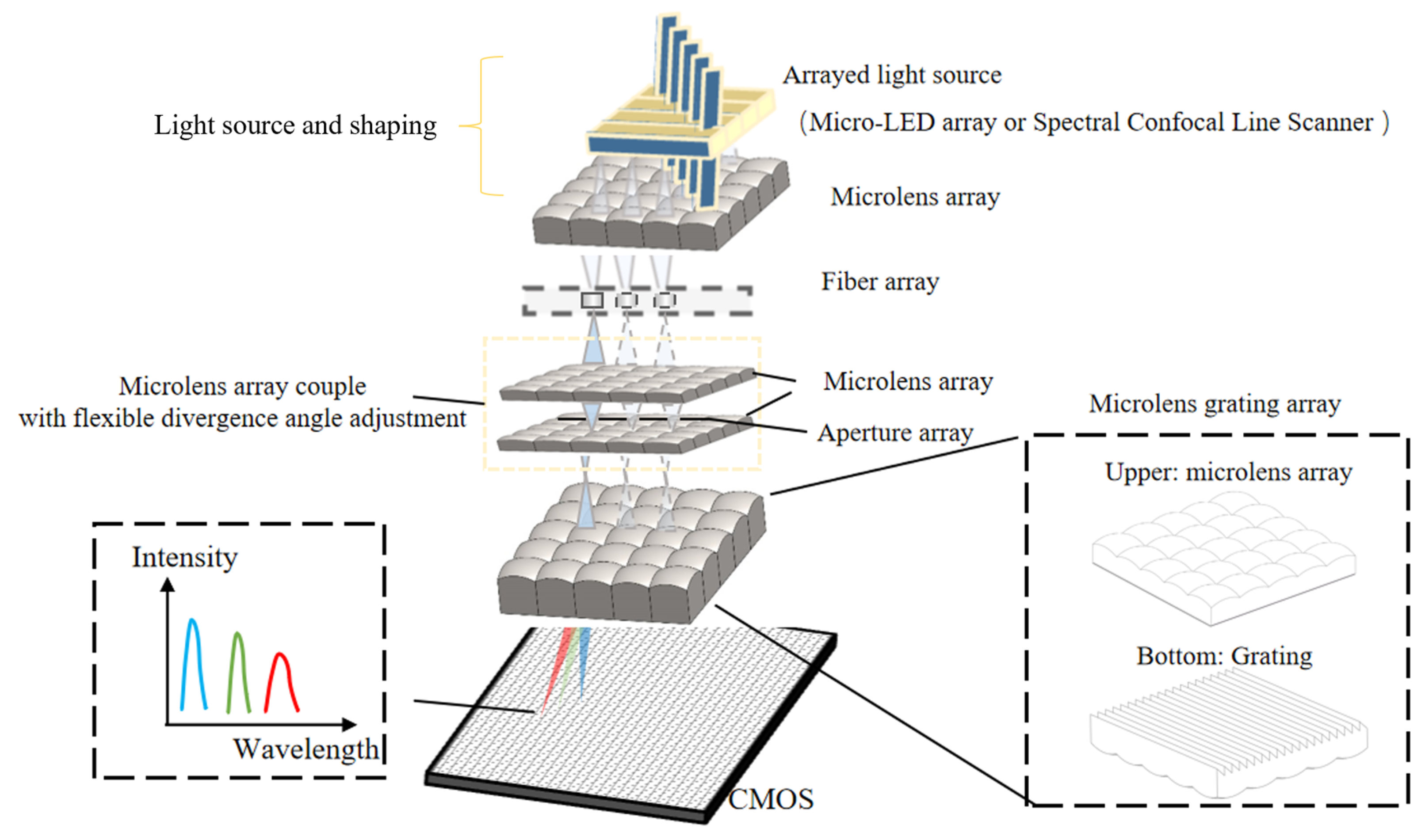
Figure 1. Schematic diagram of the structure of the array multi-channel spectrometer system.
Sensors 25 04833 g001
Figure 2. Optical path design of single channel spectrometer. θ 1 and θ 2 represent the divergence angles of the light beam at ML1 and MLAG, respectively; h 1 , h 2 , and h 3 denote the beam widths at ML1, ML2, and MLAG, respectively; f 2 and f 3 are the focal lengths of ML2 and the MLAG lens elements, respectively; and d 1 , d 2 , and d 3 are the distances between key components.
Sensors 25 04833 g002
Figure 3. Optical path of array multi-channel spectrometer system: (a) optical path model of the array spectrometer system; (b) actual picture of the array spectrometer system. MLA: Microlens Array; MLAG: Microlens Array Grating; CMOS: Complementary Metal-Oxide-Semiconductor.
Sensors 25 04833 g003
Figure 4. Component consistency test: (a) MLAG consistency test optical path; (b) MLAG consistency imaging results.
Sensors 25 04833 g004
Figure 5. Spectrometer performance test: (a) spectrometer imaging results; (b) spectral signal extraction.
Sensors 25 04833 g005
Figure 6. Data correction results.
Sensors 25 04833 g006
Figure 7. Image enhancement effects: (a) 520 nm; (b) 450 nm.
Sensors 25 04833 g007
Figure 8. Image enhancement process: (a) original grayscale image; (b) contrast enhancement; (c) nonlinear transformation; and (d) filtering out low-brightness pixels.
Sensors 25 04833 g008
Table 1. Uniformity of the MLAG surface (pixels).
No.X IntervalY Interval
1564563
2577574
3573576
4576568
5584580
6575573
CV (%)1.251.11
Table 2. Comparison of the standard deviation of diffracted light shift under different filtering effects (pixels).
Parameter CombinationFull Width at Half MaximumSD of Pixel Center Distance
MeanSD520 nm450 nm
110.5651.6260.5270.575
27.9571.5180.5480.594
35.9131.6080.5520.585
Disclaimer/Publisher’s Note: The statements, opinions and data contained in all publications are solely those of the individual author(s) and contributor(s) and not of MDPI and/or the editor(s). MDPI and/or the editor(s) disclaim responsibility for any injury to people or property resulting from any ideas, methods, instructions or products referred to in the content.