
The Design of a Computer Vision Sensor Based on a Low-Power Edge Detection Circuit


Abstract
1. Introduction
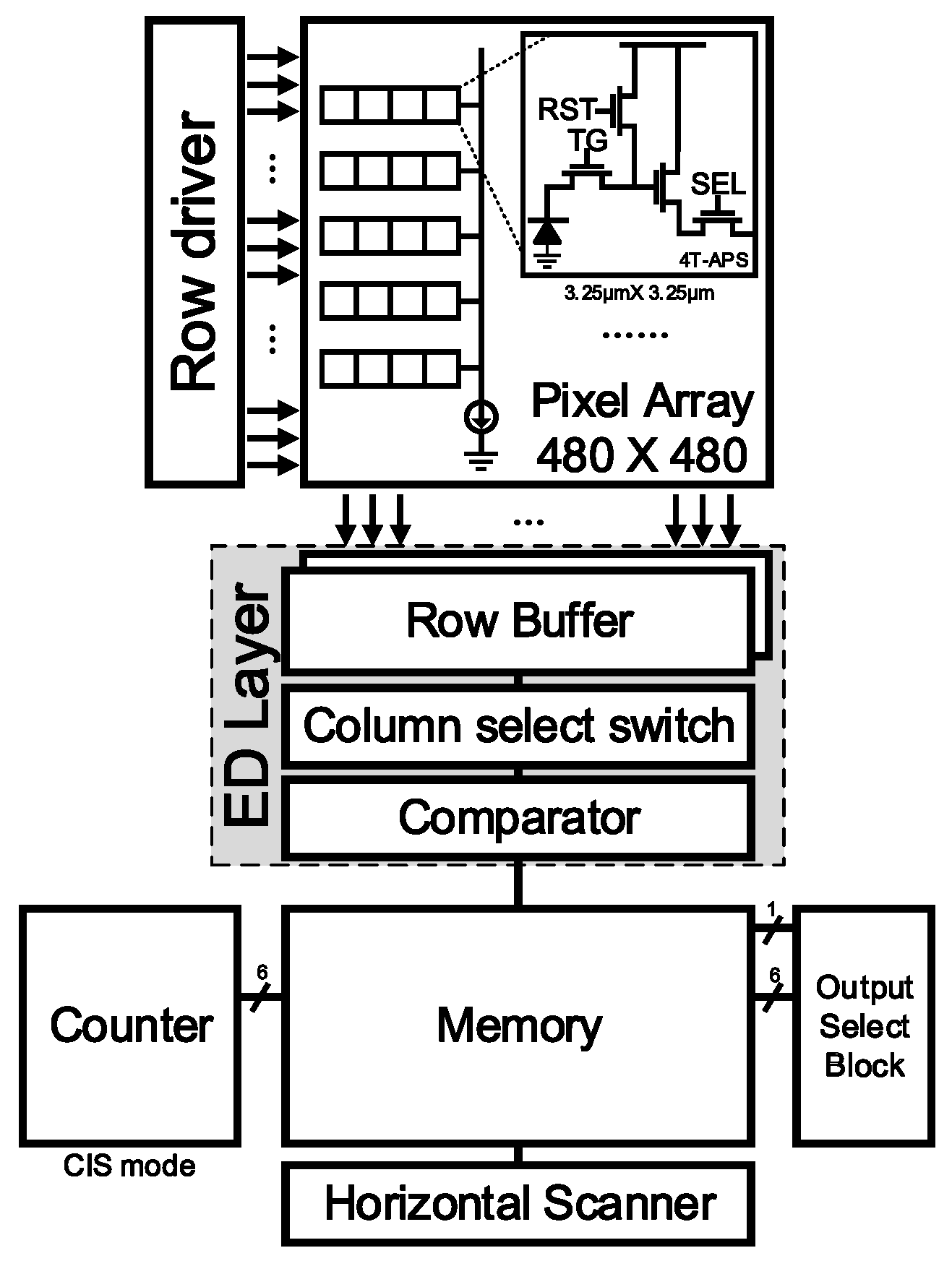
2. The Proposed CIS for Low-Power Edge Detection
2.1. Architecture Flow
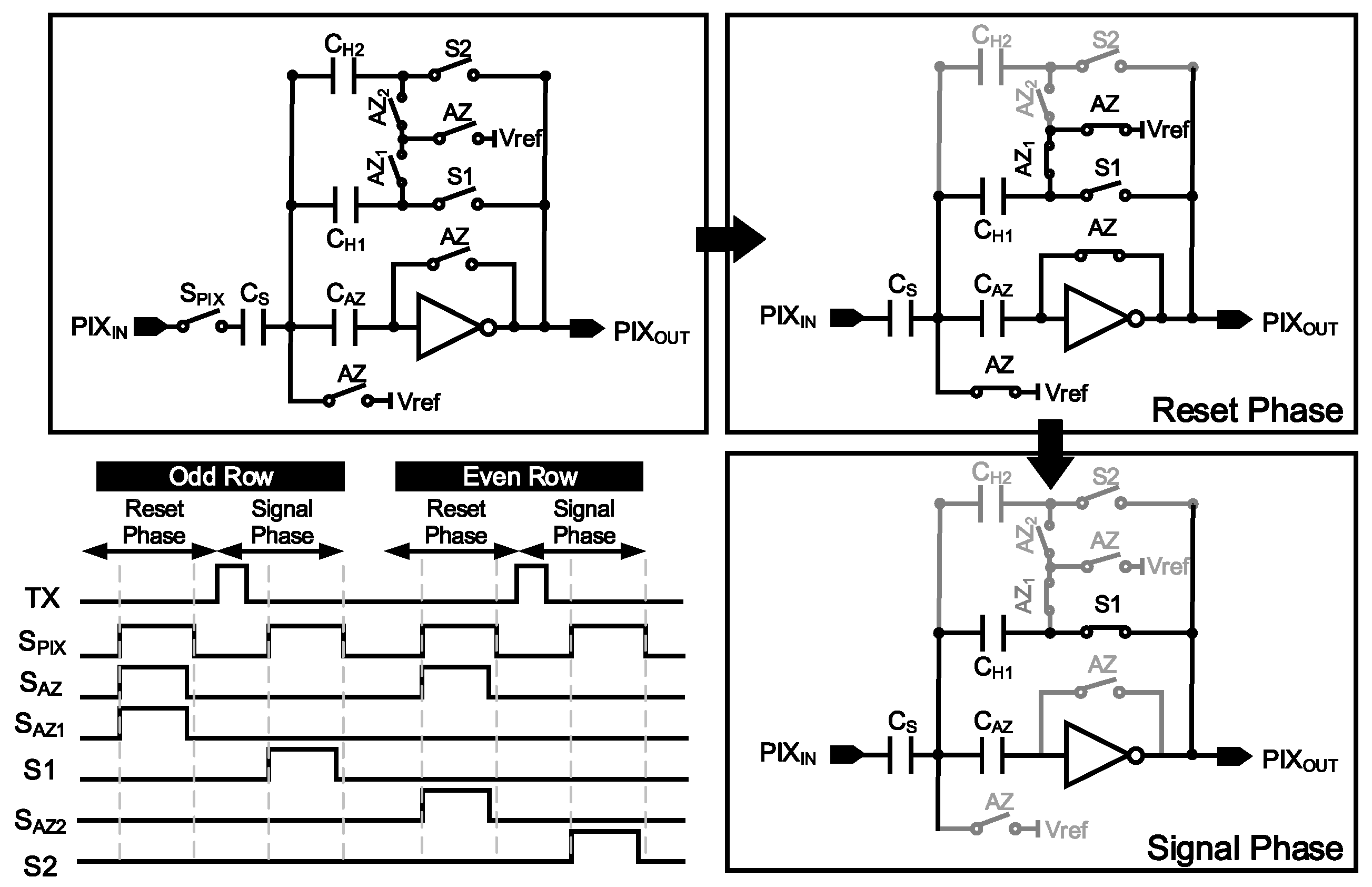
2.2. Pixel Voltage Sampling and Edge Mask Operation
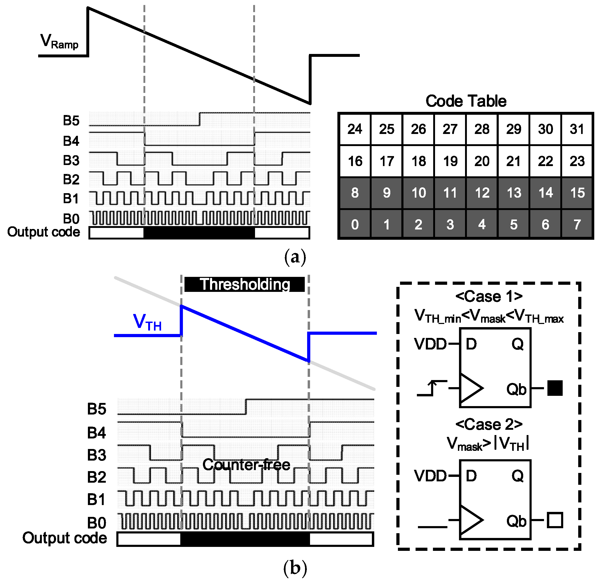
2.3. Thresholding Operation
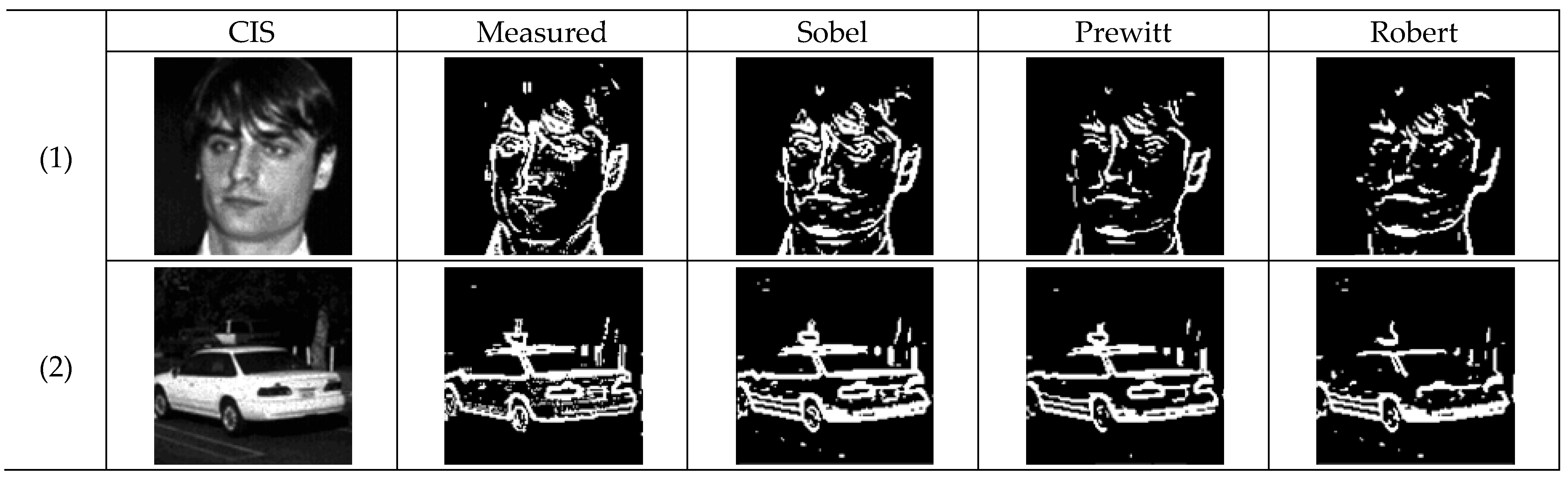
3. Experimental Results
3.1. Layout and Chip Photograph of the Proposed CIS
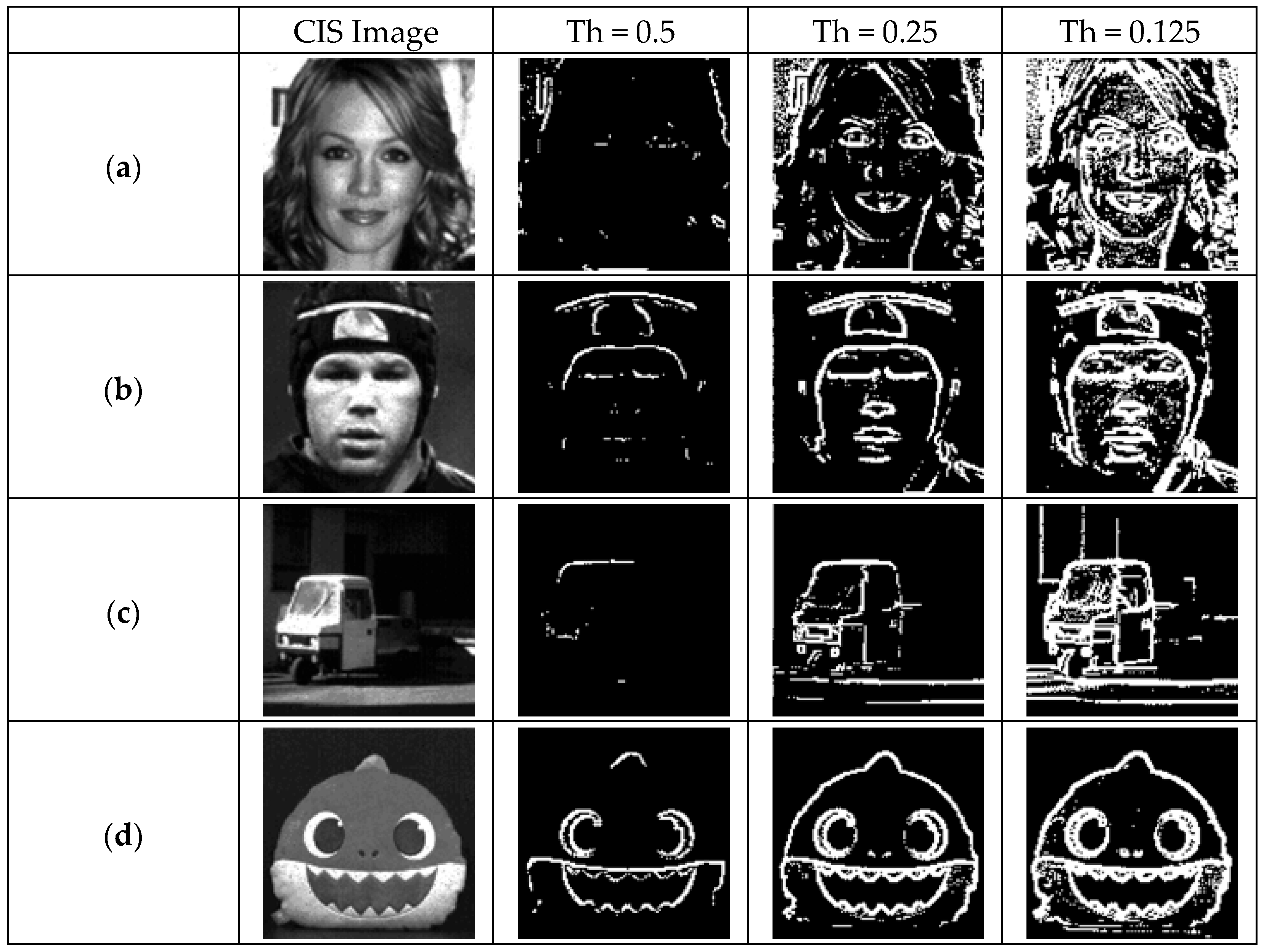
3.2. Measurement Results
4. Conclusions
Author Contributions
Funding
Institutional Review Board Statement
Informed Consent Statement
Data Availability Statement
Acknowledgments
Conflicts of Interest
References
- Singh, A.; Singh, M.; Singh, B. Face detection and eyes extraction using sobel edge detection and morphological operations. In Proceedings of the 2016 Conference on Advances in Signal Processing (CASP), Pune, India, 9–11 June 2016; pp. 295–300. [Google Scholar] [CrossRef]
- Vizoni, M.V.; Marana, A.N. Ocular Recognition Using Deep Features for Identity Authentication. In Proceedings of the 2020 International Conference on Systems, Signals and Image Processing (IWSSIP), Niteroi, Brazil, 1–3 July 2020; pp. 155–160. [Google Scholar]
- Andrei, M.-A.; Boiangiu, C.-A.; Tarbă, N.; Voncilă, M.-L. Robust Lane Detection and Tracking Algorithm for Steering Assist Systems. Machines 2022, 10, 10. [Google Scholar] [CrossRef]
- Kim, J.-H.; Kim, C.; Kim, K.; Yoo, H.-J. An Ultra-Low-Power Analog-Digital Hybrid CNN Face Recognition Processor Integrated with a CIS for Always-on Mobile Devices. In Proceedings of the 2019 IEEE International Symposium on Circuits and Systems (ISCAS), Sapporo, Japan, 26–29 May 2019; pp. 1–5. [Google Scholar] [CrossRef]
- Jin, M.; Noh, H.; Song, M.; Kim, S.Y. Design of an Edge-Detection CMOS Image Sensor with Built-in Mask Circuits. Sensors 2020, 20, 3649. [Google Scholar] [CrossRef] [PubMed]
- Lee, H.; Lee, K.; Kim, S.Y. Input-Signal-Based Power-Gated Single-Slope ADC for Low-Power CMOS Image Sensors. J. Integr. Circuits Syst. 2025, 11, 11–16. [Google Scholar] [CrossRef]
- Kim, H.-J.; Hwang, S.-I.; Chung, J.-H.; Park, J.-H.; Ryu, S.-T. A Dual-Imaging Speed-Enhanced CMOS Image Sensor for Real-Time Edge Image Extraction. IEEE J. Solid-State Circuits 2017, 52, 2488–2497. [Google Scholar] [CrossRef]
- Park, M.-J.; Kim, H.-J. A Real-Time Edge-Detection CMOS Image Sensor for Machine Vision Applications. IEEE Sens. J. 2023, 23, 9254–9261. [Google Scholar] [CrossRef]
- Lee, S.; Jeong, B.; Park, K.; Song, M.; Kim, S.Y. On-CMOS Image Sensor Processing for Lane Detection. Sensors 2021, 21, 3713. [Google Scholar] [CrossRef] [PubMed]
- Asghar, M.S.; Shah, S.A.A.; Kim, H. A Low Power Mixed Signal Convolutional Neural Network for Deep Learning SoC. J. Integr. Circuits Syst. 2023, 9, 3. Available online: https://jicas.idec.or.kr/index.php/JICAS/article/view/189 (accessed on 14 May 2025).
- Choi, J.; Lee, S.; Son, Y.; Kim, S.Y. Design of an Always-On Image Sensor Using an Analog Lightweight Convolutional Neural Network. Sensors 2020, 20, 3101. [Google Scholar] [CrossRef] [PubMed]
- Kobayashi, M.; Onuki, Y.; Kawabata, K.; Sekine, H.; Tsuboi, T.; Muto, T.; Akiyama, T.; Matsuno, Y.; Takahashi, H.; Koizumi, T.; et al. A 1.8e-rms Temporal Noise Over 110-dB-Dynamic Range 3.4 µm Pixel Pitch Global-Shutter CMOS Image Sensor with Dual-Gain Amplifiers SS-ADC, Light Guide Structure, and Multiple-Accumulation Shutter. IEEE J. Solid-State Circuits 2018, 53, 219–228. [Google Scholar] [CrossRef]
- Fernández Maimó, L.; Huertas Celdrán, A.; Perales Gómez, Á.L.; García Clemente, F.J.; Weimer, J.; Lee, I. Intelligent and Dynamic Ransomware Spread Detection and Mitigation in Integrated Clinical Environments. Sensors 2019, 19, 1114. [Google Scholar] [CrossRef] [PubMed]
- Young, C.; Omid-Zohoor, A.; Lajevardi, P.; Murmann, B. A Data-Compressive 1.5/2.75-bit Log-Gradient QVGA Image Sensor With Multi-Scale Readout for Always-On Object Detection. IEEE J. Solid-State Circuits 2019, 54, 2932–2946. [Google Scholar] [CrossRef]
- Poobathy, D.; Chezian, R. Edge Detection Operators: Peak Signal to Noise Ratio Based Comparison. Int. J. Image Graph. Signal Process. 2014, 6, 55–61. [Google Scholar] [CrossRef]


| Process | Voffset [mV] | Open Loop Gain [dB] | Unity Gain Frequency [MHz] |
|---|---|---|---|
| ff | 6.39 | 71.3 | 59.3 |
| nn | 8.50 | 72.2 | 46.1 |
| ss | 11.4 | 72.1 | 35.9 |
| MSE | (1) | (2) |
|---|---|---|
| Sobel | 0.14 | 0.12 |
| Prewitt | 0.11 | 0.10 |
| Robert | 0.15 | 0.12 |
| PSNR [dB] | (1) | (2) |
|---|---|---|
| Sobel | 56.66 | 57.17 |
| Prewitt | 57.65 | 58.16 |
| Robert | 56.38 | 57.35 |
| Accuracy [%] | (1) | (2) |
|---|---|---|
| Sobel | 90% | 92% |
| Prewitt | 90% | 93% |
| Robert | 86% | 87% |
| Process | 0.11 μm 1P6M CIS process |
| Pixel size | 3.25 μm |
| Pixel type | 4T-APS |
| Pixel resolution | 120 |
| Chip area | 4.3 mm |
| Core area | 1.923 mm |
| Supply voltages | 2.8V,1.5V(Analog)/1.5V(Digital) |
| ADC resolution | 1bit (5-bit ADC-comparable accuracy) |
| Clock frequency | 10 MHz |
| Power consumption | 1.52 mW |
| FPS | 235 @ Edge detection mode 220 @ CIS mode |
| [5] | [7] | [9] | This work | |
| Edge Image |  |  |  | 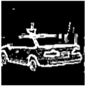 |
| Progress | 0.09 μm 1P4M CIS | 0.18 μm 1P4M CIS | 0.11 μm 1P4M CIS | 0.11 μm 1P6M CIS |
| Resolution | 1440 | 120 | 120 | 120 |
| Pixel pitch | 1.4 μm | 4.9 μm | 3.2 μm | 3.25 μm |
| Supply voltage | 2.8 V (Pixel)/3.3 V (Analog)/1.2 V (Digital) | 2.8 V (Pixel)/1.8 V (Circuit) | 3.3 V (Pixel, Analog) 1.5 V (Digital) | 3.3 V (Pixel)/2.8 V (Analog)/1.5 V (Analog, Digital) |
| Power | 9.4 mW | 4.3 mW | 9.4 mW | 1.52 mW |
| FPS | 60 | 3200 | 145 | 235 |
| * FoM [pJ/pixel/frame] | 56.7 | 70 | 3376.4 | ** 449.2 |
Disclaimer/Publisher’s Note: The statements, opinions and data contained in all publications are solely those of the individual author(s) and contributor(s) and not of MDPI and/or the editor(s). MDPI and/or the editor(s) disclaim responsibility for any injury to people or property resulting from any ideas, methods, instructions or products referred to in the content. |
© 2025 by the authors. Licensee MDPI, Basel, Switzerland. This article is an open access article distributed under the terms and conditions of the Creative Commons Attribution (CC BY) license (https://creativecommons.org/licenses/by/4.0/).
Share and Cite
Lee, S.; Yun, Y.C.; Heu, S.M.; Lee, K.H.; Lee, S.J.; Lee, K.; Moon, J.; Lim, H.; Jang, T.; Song, M.; et al. The Design of a Computer Vision Sensor Based on a Low-Power Edge Detection Circuit. Sensors 2025, 25, 3219. https://doi.org/10.3390/s25103219
Lee S, Yun YC, Heu SM, Lee KH, Lee SJ, Lee K, Moon J, Lim H, Jang T, Song M, et al. The Design of a Computer Vision Sensor Based on a Low-Power Edge Detection Circuit. Sensors. 2025; 25(10):3219. https://doi.org/10.3390/s25103219
Chicago/Turabian StyleLee, Suhyeon, Yu Chan Yun, Seung Min Heu, Kyu Hyun Lee, Seung Joon Lee, Kyungmin Lee, Jiin Moon, Hyuna Lim, Taeun Jang, Minkyu Song, and et al. 2025. "The Design of a Computer Vision Sensor Based on a Low-Power Edge Detection Circuit" Sensors 25, no. 10: 3219. https://doi.org/10.3390/s25103219
APA StyleLee, S., Yun, Y. C., Heu, S. M., Lee, K. H., Lee, S. J., Lee, K., Moon, J., Lim, H., Jang, T., Song, M., & Kim, S. Y. (2025). The Design of a Computer Vision Sensor Based on a Low-Power Edge Detection Circuit. Sensors, 25(10), 3219. https://doi.org/10.3390/s25103219