
Advancing Understanding of High-Temperature Micro-Electro-Mechanical System Failures with New Simulation-Assisted Approach


Abstract
1. Introduction
1.1. High-Temperature MEMS Performance
1.2. Atomic Migration as a Failure Mechanism
2. Materials and Methods
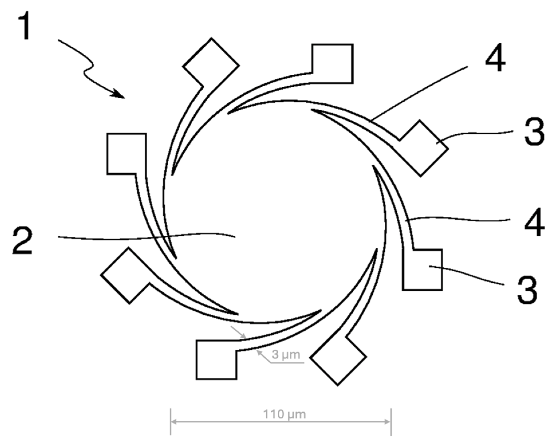
2.1. Tungsten MEMS Hotplates
2.2. Vacancy Flux Model
- A vacancy flux due to the electric field:
- A vacancy flux due to the temperature gradient:
- A vacancy flux due to the hydrostatic stress gradient:
2.3. Simulation Model Development
- Solid Mechanics;
- Electric Currents;
- Heat Transfer in Solids;
- Multiphysics;
- Transport in Solids.
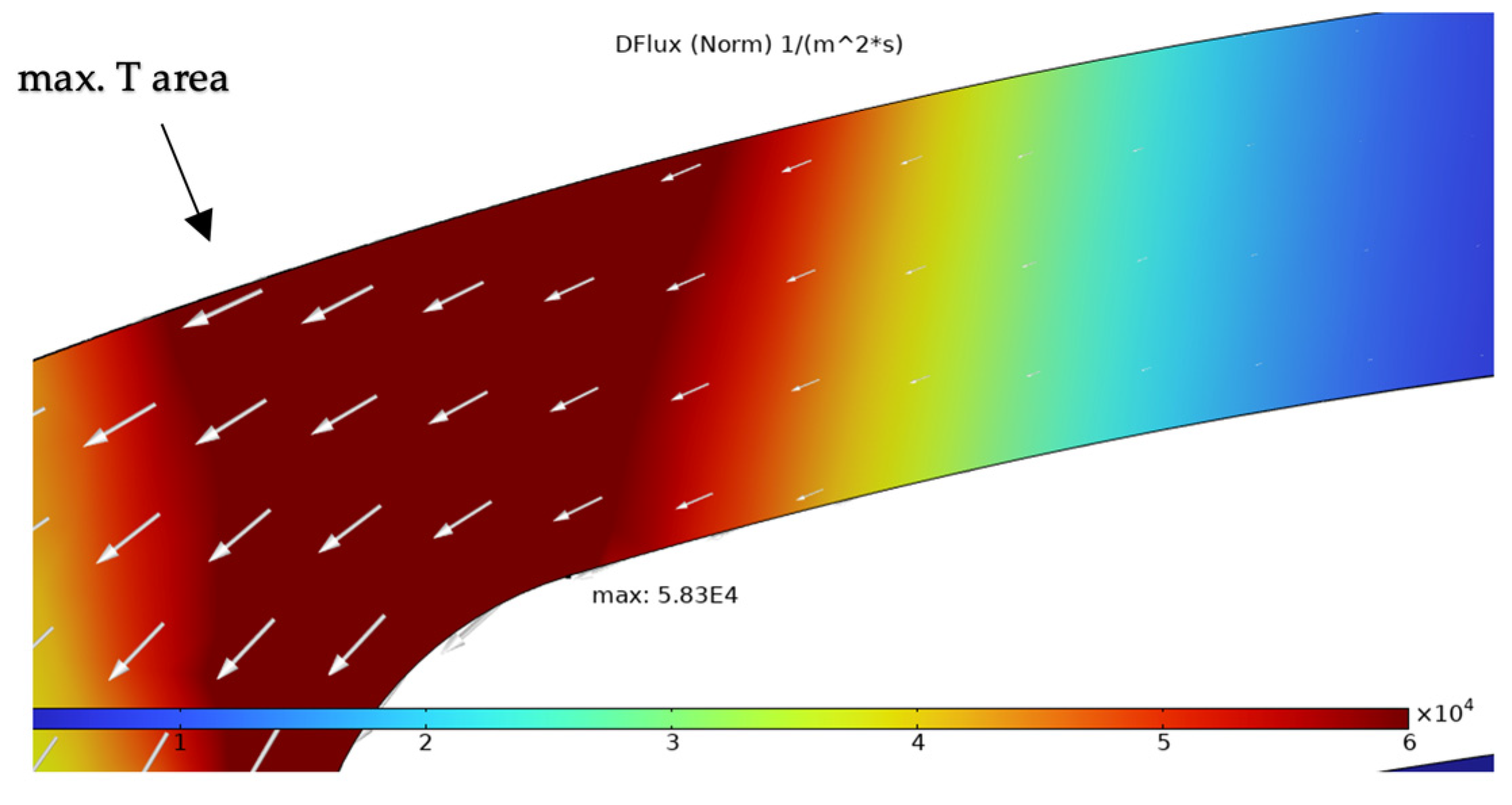
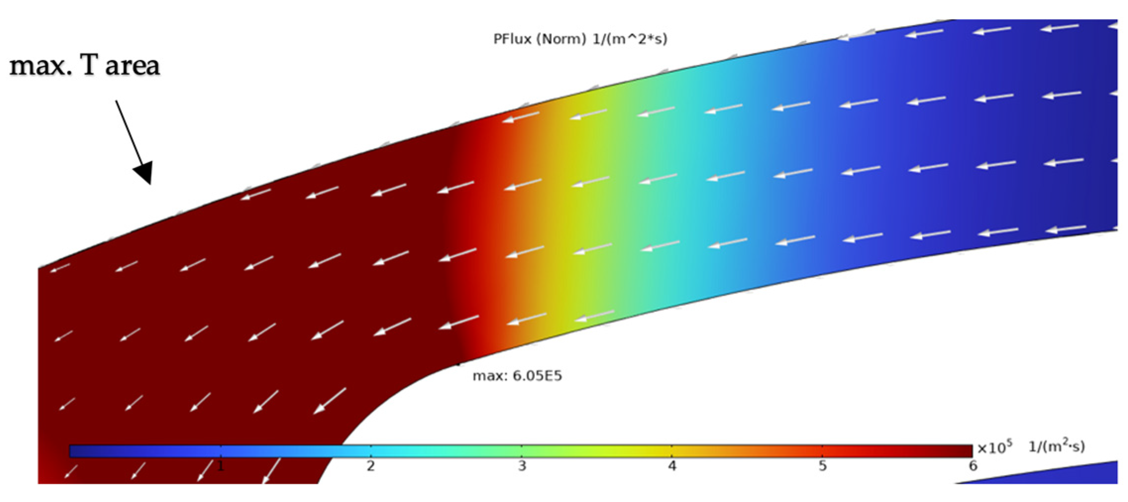
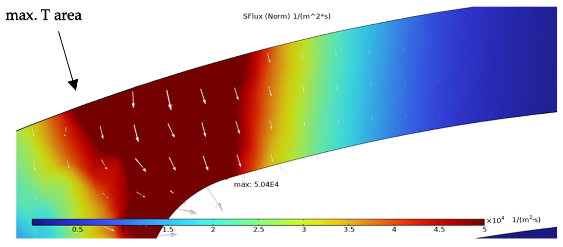
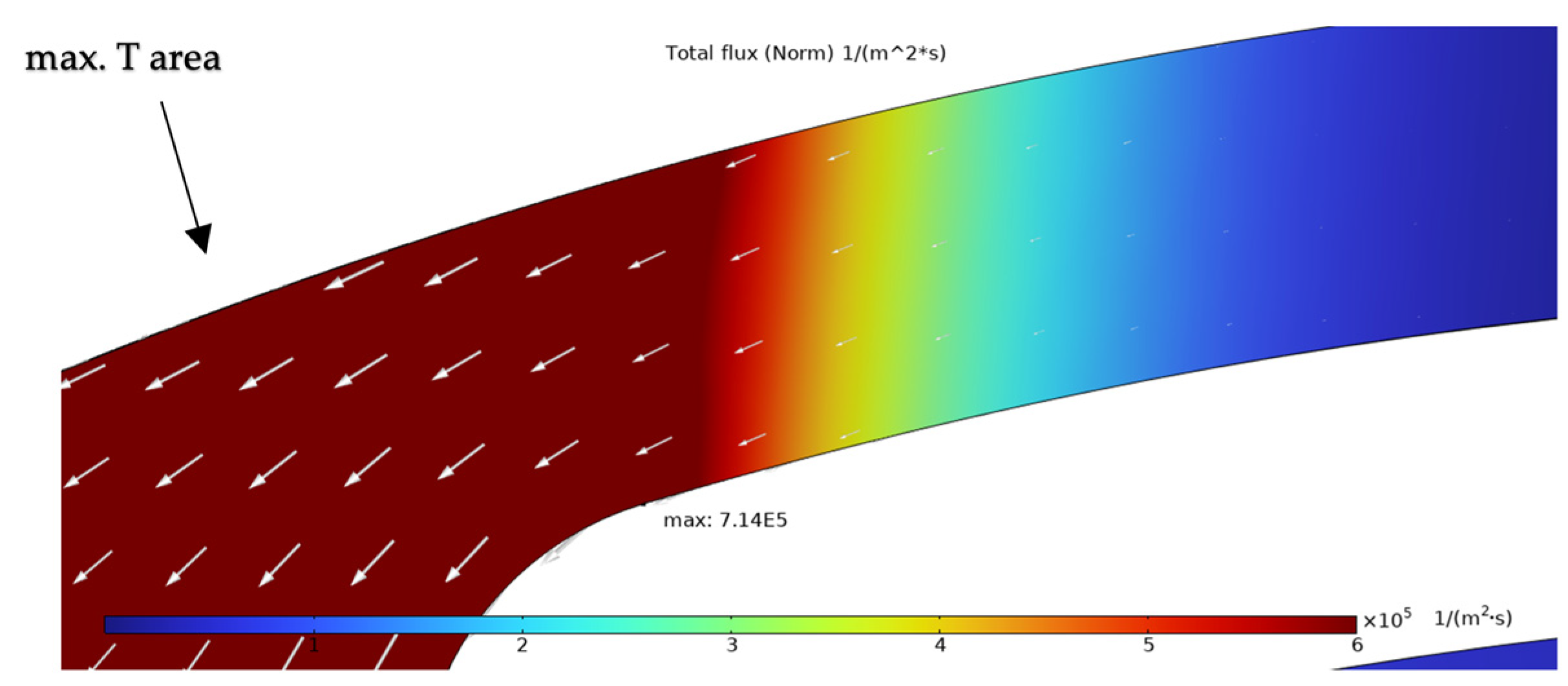
3. Results
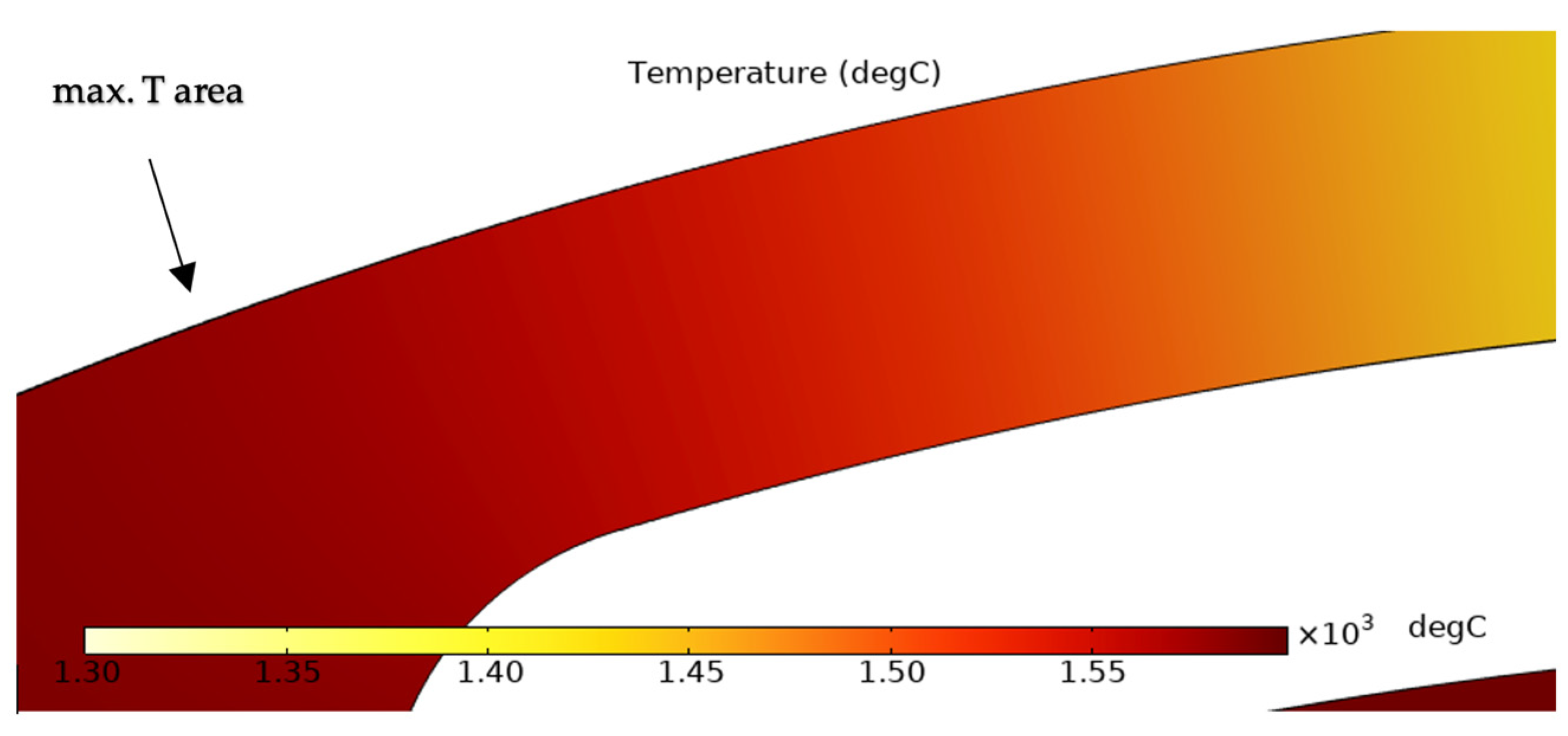
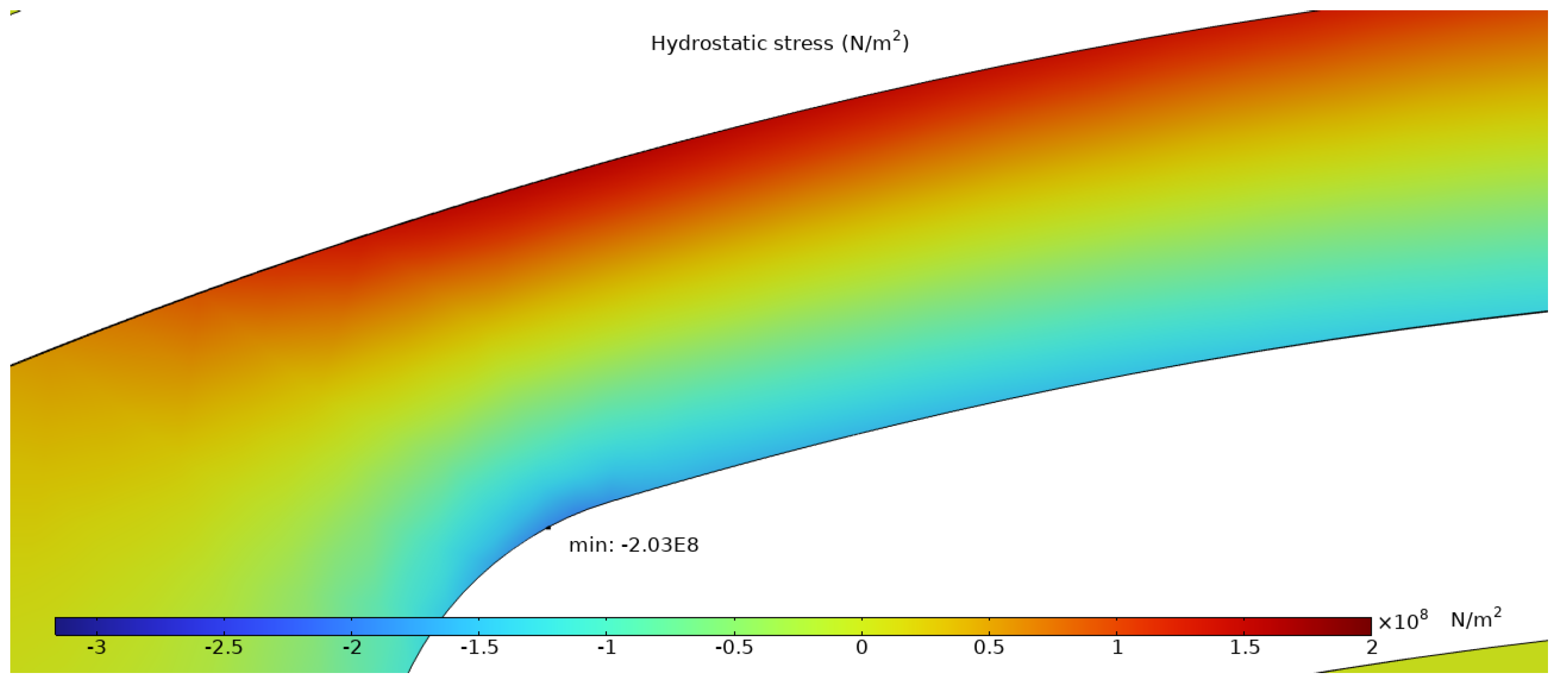
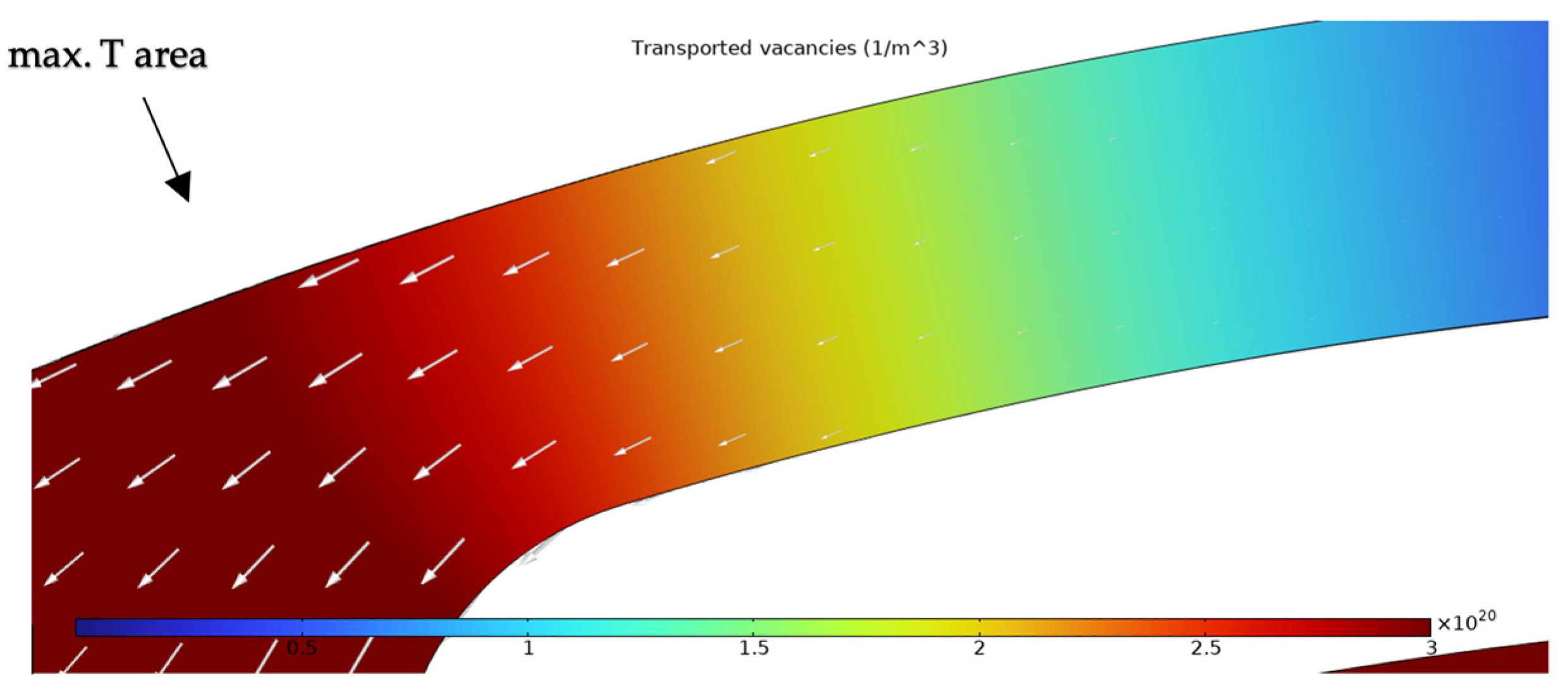
Simulation Results
4. Discussion
5. Summary
Author Contributions
Funding
Institutional Review Board Statement
Informed Consent Statement
Data Availability Statement
Acknowledgments
Conflicts of Interest
Nomenclature
| D | Diffusivity |
| Pre-exponential factor | |
| Grain boundary diffusion activation energy | |
| Vacancy formation energy | |
| Electric field | |
| G | Generation or annihilation source |
| Total vacancy flux | |
| M | Molar mass |
| N | Total number of atomic sites |
| Avogadro constant | |
| Q* | Heat of transport |
| T | Temperature |
| V | Voltage |
| Z* | Effective charge number |
| c | Concentration |
| Vacancy concentration | |
| Initial vacancy concentration | |
| Equilibrium vacancy concentration | |
| e | Elementary charge |
| f | Vacancy relaxation factor |
| k | Boltzmann constant |
| x | Coordinate |
| t | Time |
| Ω | Atomic volume |
| ρ | Mass density |
| Hydrostatic stress | |
| Von Mises stress | |
| Vacancy relaxation time |
References
- Nagaiah, N.R.; Sleiti, A.K.; Rodriguez, S.; Kapat, J.S.; An, L.; Chow, L. A novel design and analysis of a MEMS ceramic hot-wire anemometer for high temperature applications. J. Phys. Conf. Ser. 2006, 34, 277–282. [Google Scholar] [CrossRef]
- Esteves, G.; Habermehl, S.D.; Clews, P.J.; Fritch, C.; Griffin, B.A. AlN/SiC MEMS for High-Temperature Applications. J. Microelectromech. Syst. 2019, 28, 859–864. [Google Scholar] [CrossRef]
- Lee, K.-N.; Lee, D.-S.; Jung, S.-W.; Jang, Y.-H.; Kim, Y.-K.; Seong, W.-K. A high-temperature MEMS heater using suspended silicon structures. J. Micromech. Microeng. 2009, 19, 115011. [Google Scholar] [CrossRef]
- Spannhake, J.; Helwig, A.; Müller, G.; Faglia, G.; Sberveglieri, G.; Doll, T.; Wassner, T.; Eickhoff, M. SnO₂:Sb—A new material for high-temperature MEMS heater applications: Performance and limitations. Sens. Actuators B Chem. 2007, 124, 421–428. [Google Scholar] [CrossRef]
- Lee, S.M.; Dyer, D.C.; Gardner, J.W. Design and optimisation of a high-temperature silicon micro-hotplate for nanoporous palladium pellistors. Microelectron. J. 2003, 34, 115–126, ISSN 1879-2391. [Google Scholar] [CrossRef]
- Schössler, T.; Schön, F.; Lemier, C.; Urban, G. Reliability improvements of thin film platinum resistors on wafer-level and micro-hotplates at stress temperatures in the range of 140–290 °C. Microelectron. Reliab. 2020, 104, 113557. [Google Scholar] [CrossRef]
- Biró, F.; Dücso, C.; Hajnal, Z.; Riesz, F.; Pap, A.E.; Bársony, I. Thermo-mechanical design and characterization of low dissipation micro-hotplates operated above 500 °C. Microelectron. J. 2015, 45, 1822–1828. [Google Scholar] [CrossRef]
- Rydberg, M.; Smith, U. Long-term stability and electrical properties of fluorine doped polysilicon IC-resistors. Mater. Sci. Semicond. Process. 2001, 4, 373–382. [Google Scholar] [CrossRef]
- Creemer, J.F.; Briand, D.; Zandbergen, H.; van der Vlist, W.; de Boer, C.; de Rooij, N.; Sarro, P. Microhotplates with TiN heaters. Sens. Actuators A Phys. 2008, 148, 416–421. [Google Scholar] [CrossRef]
- Castagna, M.E.; Modica, R.; Cascino, S.; Moschetti, M.; Cerantonio, V.; Messina, A.; Santangelo, A. A high stability and uniformity W micro hot plate. Sens. Actuators A Phys. 2018, 279, 617–623. [Google Scholar] [CrossRef]
- Zhou, J.; Yu, J.; Li, Z.; Liu, K.; Tang, Z. High temperature reliability and failure of W-based microhotplates. In Proceedings of the 2015 IEEE SENSORS, Busan, Republic of Korea, 1–4 November 2015. [Google Scholar]
- Ali, S.Z.; Udrea, F.; Milne, W.I.; Gardner, J.W. Tungsten-based SOI microhotplates for smart gas sensors. J. Microelectromech. Syst. 2008, 17, 1408–1417. [Google Scholar] [CrossRef]
- Yu, J.; Li, Z.; Yao, G.; Zhu, H.; Huang, Z.; Tang, Z. Stability and Failure Analysis of a W-Based Microhotplate. J. Microelectromech. Syst. 2022, 31, 951–959. [Google Scholar] [CrossRef]
- Bíró, F.; Hajnal, Z.; Dücső, C.; Bársony, I. The critical impact of temperature gradients on Pt filament failure. Microelectron. Reliab. 2017, 78, 118–125. [Google Scholar] [CrossRef]
- Mele, L.; Santagata, F.; Iervolino, E.; Mihailovic, M.; Rossi, T.; Tran, A.; Schellevis, H.; Creemer, J.; Sarro, P. A molybdenum MEMS microhotplate for high-temperature operation. Sens. Actuators A Phys. 2012, 188, 173–180. [Google Scholar] [CrossRef]
- Thomas, E.L.H.; Stritt, J.; Mandal, S.; Imboden, M.; Williams, O.A. Polycrystalline Diamond Micro-Hotplates. Small 2023, 19, 2303976. [Google Scholar] [CrossRef]
- Fung, S.K.H.; Tang, Z.; Chan, P.C.H.; Sin, J.K.O.; Cheung, P.W. Thermal analysis and design of a micro-hotplate for integrated gas-sensor applications. In Proceedings of the International Solid-State Sensors and Actuators Conference—TRANSDUCERS ’95, Stockholm, Sweden, 25–29 June 1995. [Google Scholar]
- Liu, Q.; Wang, Y.; Yao, J.; Ding, G. Impact resistance and static strength analysis of an extremely simplified micro hotplate with novel suspended film. Sens. Actuators A Phys. 2018, 280, 495–504. [Google Scholar] [CrossRef]
- Filipovic, L. Theoretical examination of thermo-migration in novel platinum microheaters. Microelectron. Reliab. 2021, 123, 114219. [Google Scholar] [CrossRef]
- de Orio, R.L. Electromigration Modeling and Simulation. Ph.D. Thesis, Technische Universität Wien, Vienna, Austria, 2010. [Google Scholar]
- Lienig, M.; Thiele, J. Fundamentals of Electromigration. In Fundamentals of Electromigration-Aware Integrated Circuit Design; Springer International Publishing: Cham, Switzerland, 2018; pp. 13–60. [Google Scholar] [CrossRef]
- Kraft, O.; Sanchez, J.E.; Bauer, M.; Arzt, E. Quantitative analysis of electromigration damage in Al-based conductor lines. J. Mater. Res. 1997, 12, 2027–2037. [Google Scholar] [CrossRef]
- Imboden, M. High-Temperature Infrared Radiator Element and Methods. US20210176828A1. 2019.
- Imboden, M. Infrared Radiator Element and Methods. US20230131181A1. 2021.
- Smallman, R.E.; Bishop, R.J. Modern Physical Metallurgy and Materials Engineering; Butterworth-Heinemann: Oxford, UK, 1999. [Google Scholar]
- Lee, J.S.; Minkwitz, C.; Herzig, C. Grain boundary self-diffusion in polycrystalline tungsten at low temperatures. Phys. Status Solidi B 1997, 202, 931–940. [Google Scholar] [CrossRef]
- Kanapady, R.; Moore, D.; Raghupathy, A.; Maltz, W. Influence of Temperature Gradient on the Electromigration-Failures in 3D Packaging. In Proceedings of the 2016 15th IEEE Intersociety Conference on Thermal and Thermomechanical Phenomena in Electronic Systems (ITherm), Las Vegas, NV, USA, 31 May–3 June 2016. [Google Scholar]
- Petersson, C.L.M.; Fredriksson, A.; Melin, S.; Ahadi, A.; Hansson, P. A molecular dynamics study on the influence of vacancies and interstitial helium on mechanical properties of tungsten. J. Nucl. Mater. 2023, 580, 154378. [Google Scholar] [CrossRef]
- Li, Z.Z.; Li, Y.-H.; Ren, Q.-Y.; Ma, F.-F.; Yue, F.-Y.; Zhou, H.-B.; Lu, G.-H. Strain dependence of energetics and kinetics of vacancy in Tungsten. Materials 2020, 13, 3375. [Google Scholar] [CrossRef] [PubMed]
- NIST Chemistry WebBook. Available online: https://webbook.nist.gov/cgi/cbook.cgi?ID=C7440337&Mask=1E9F (accessed on 23 May 2024).
- Mundy, J.N.; Rothman, S.J.; Lam, N.Q.; Hoff, H.A.; Nowicki, L.J. Self-diffusion in tungsten. Phys. Rev. B 1978, 18, 6566. [Google Scholar] [CrossRef]
- Yakunkin, M.M. Mechanism of High-Temperature Heat Capacity of Tungsten: Study of Relaxation Processes. Phys. Solid State 2004, 46, 218–223. [Google Scholar] [CrossRef]
- Li, S.; Sellers, M.S.; Basaran, C.; Schultz, A.J.; Kofke, D.A. Lattice strain due to an atomic vacancy. Int. J. Mol. Sci. 2009, 10, 2798–2808. [Google Scholar] [CrossRef]


| Heater Material | Temperature Reached at the Time of Failure | Failure Mechanism | Reference |
|---|---|---|---|
| Pt | 870 °C | Hotspot formation | [5] |
| Pt | 700 °C | Electromigration | [7] |
| W | 750 °C | Rupture of membrane | [11] |
| Pt | 820 °C | Electromigration | [6] |
| TiN | 720 °C | Rupture of membrane | [9] |
| Al | 350 °C | Hotspot formation | [17] |
| Pt | 550 °C | Displacement of suspended structures | [18] |
| W | 850 °C | Electromigration and stress migration | [13] |
| Pt | 1057 °C | Thermomigration | [14] |
| Mo | 1360 °C | Rupture of membrane | [15] |
| Testing Specifications | |
|---|---|
| Voltage | 0.6 V |
| Current type | DC |
| Hotplate temperature | 1577 °C |
| Environmental Conditions | Value | Units |
|---|---|---|
| Ambient temperature | 20 | °C |
| Reference temperature | 20 | °C |
| Applied voltage | 0.59 | V |
| Parameter | Value | Units | Reference |
|---|---|---|---|
| Pre-exponential factor | [26] | ||
| Diffusion activation energy | [25,27] | ||
| Vacancy formation activation energy | [25,28,29] | ||
| Molar mass of tungsten | [30] | ||
| Vacancy relaxation ratio f | - | [31] | |
| Vacancy relaxation time | s | [32] | |
| Atomic volume | [27] | ||
| Effective valence | −20 | - | [27] |
| Heat of transport | [27] |
| Parameter | Equation | Unit | References |
|---|---|---|---|
| Diffusivity | [19,20,25] | ||
| Initial vacancy concentration | [25] | ||
| Total number of atomic sites | [25] | ||
| Equilibrium vacancy concentration | [20,33] | ||
| Source term | [20,33] | ||
| Vacancy flux due to diffusion | DFlux = | [19,20,27] | |
| Vacancy flux due to electric field | [19,20,27] | ||
| Vacancy flux due to temperature gradient | [19,20,27] | ||
| Vacancy flux due to stress gradient | [19,20,27] |
| Temperature [°C] | Current Density Norm [A/m2] | Average Current Density [A/m2] | Hydrostatic Stress (Absolute) [N/m2] |
|---|---|---|---|
| 1580 |
| DFlux (Norm) [1/(m2s)] | PFlux (Norm) [1/(m2s)] | TFlux (Norm) [1/(m2s)] | SFlux (Norm) [1/(m2s)] | Total Flux (Norm) [1/(m2s)] | |
|---|---|---|---|---|---|
| Results | |||||
| Normalized results | 8.17% | 84.73% | 0.03% | 7.06% | 100% |
Disclaimer/Publisher’s Note: The statements, opinions and data contained in all publications are solely those of the individual author(s) and contributor(s) and not of MDPI and/or the editor(s). MDPI and/or the editor(s) disclaim responsibility for any injury to people or property resulting from any ideas, methods, instructions or products referred to in the content. |
© 2025 by the authors. Licensee MDPI, Basel, Switzerland. This article is an open access article distributed under the terms and conditions of the Creative Commons Attribution (CC BY) license (https://creativecommons.org/licenses/by/4.0/).
Share and Cite
Sadurska, W.L.; Imboden, M.; Burger, J.; Dommann, A.J. Advancing Understanding of High-Temperature Micro-Electro-Mechanical System Failures with New Simulation-Assisted Approach. Sensors 2025, 25, 3120. https://doi.org/10.3390/s25103120
Sadurska WL, Imboden M, Burger J, Dommann AJ. Advancing Understanding of High-Temperature Micro-Electro-Mechanical System Failures with New Simulation-Assisted Approach. Sensors. 2025; 25(10):3120. https://doi.org/10.3390/s25103120
Chicago/Turabian StyleSadurska, Weronika Lidia, Matthias Imboden, Jürgen Burger, and Alex Jean Dommann. 2025. "Advancing Understanding of High-Temperature Micro-Electro-Mechanical System Failures with New Simulation-Assisted Approach" Sensors 25, no. 10: 3120. https://doi.org/10.3390/s25103120
APA StyleSadurska, W. L., Imboden, M., Burger, J., & Dommann, A. J. (2025). Advancing Understanding of High-Temperature Micro-Electro-Mechanical System Failures with New Simulation-Assisted Approach. Sensors, 25(10), 3120. https://doi.org/10.3390/s25103120