

A Compact and Tunable Active Inductor-Based Bandpass Filter with High Dynamic Range for UHF Band Applications


Abstract
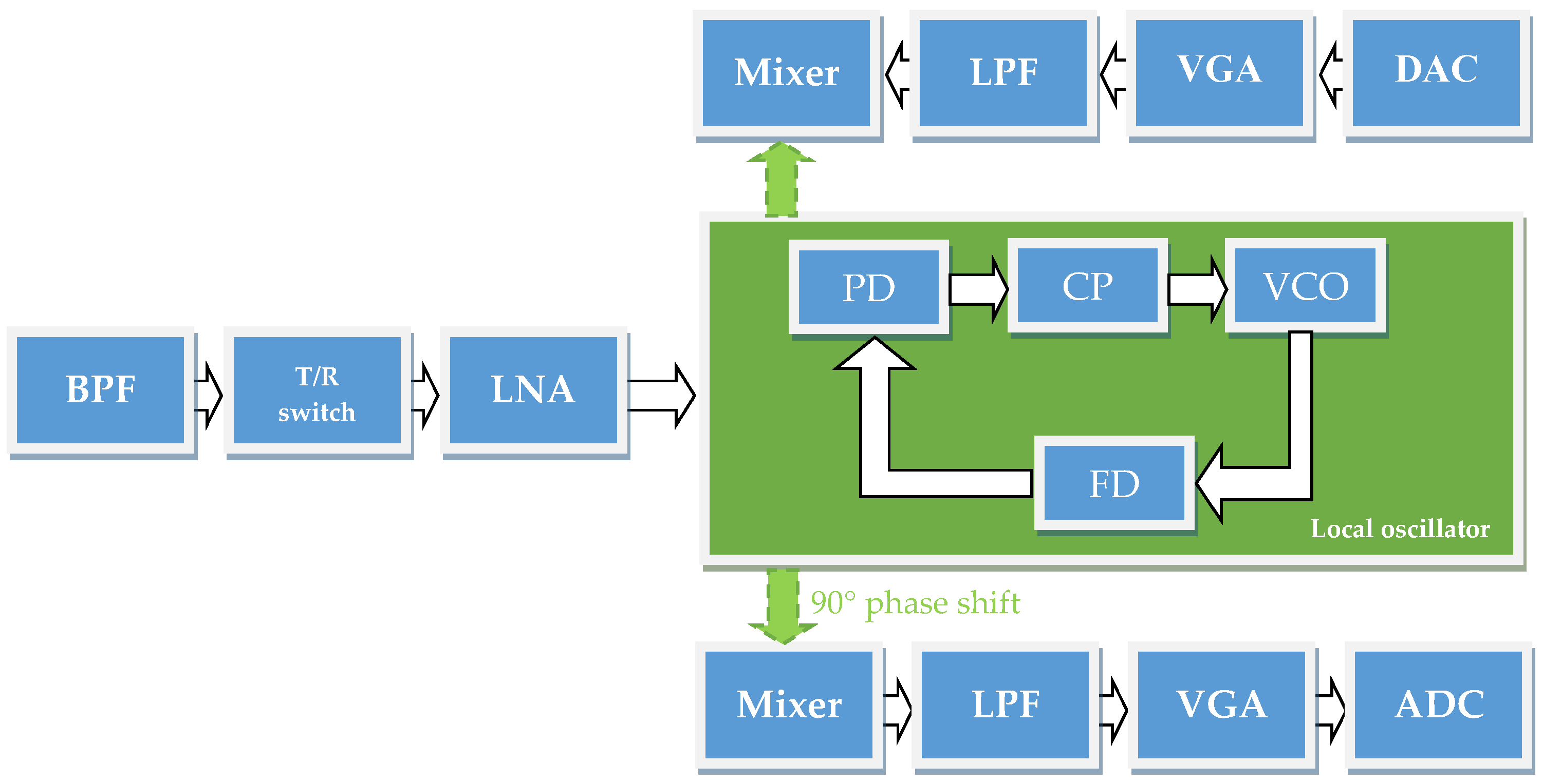
1. Introduction
2. Differential Active Inductor Design
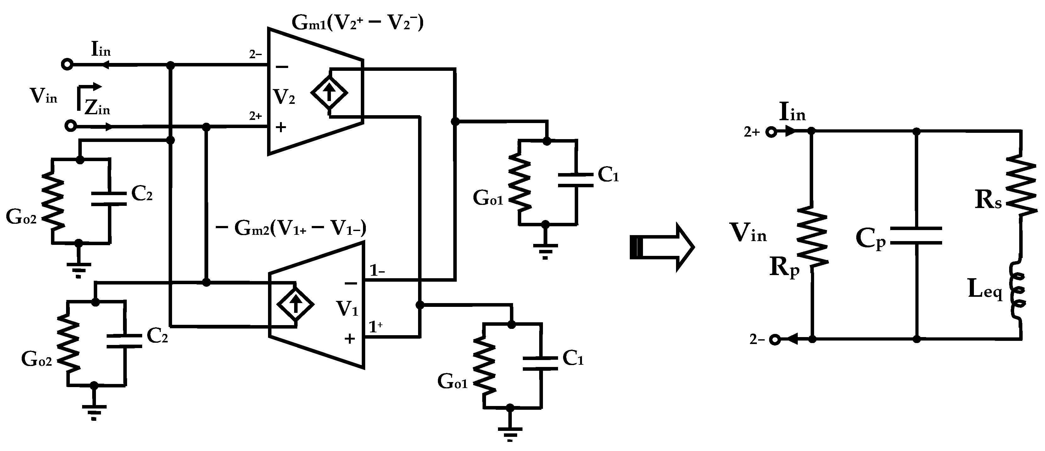
2.1. Basic Concept of Differential Active Inductors
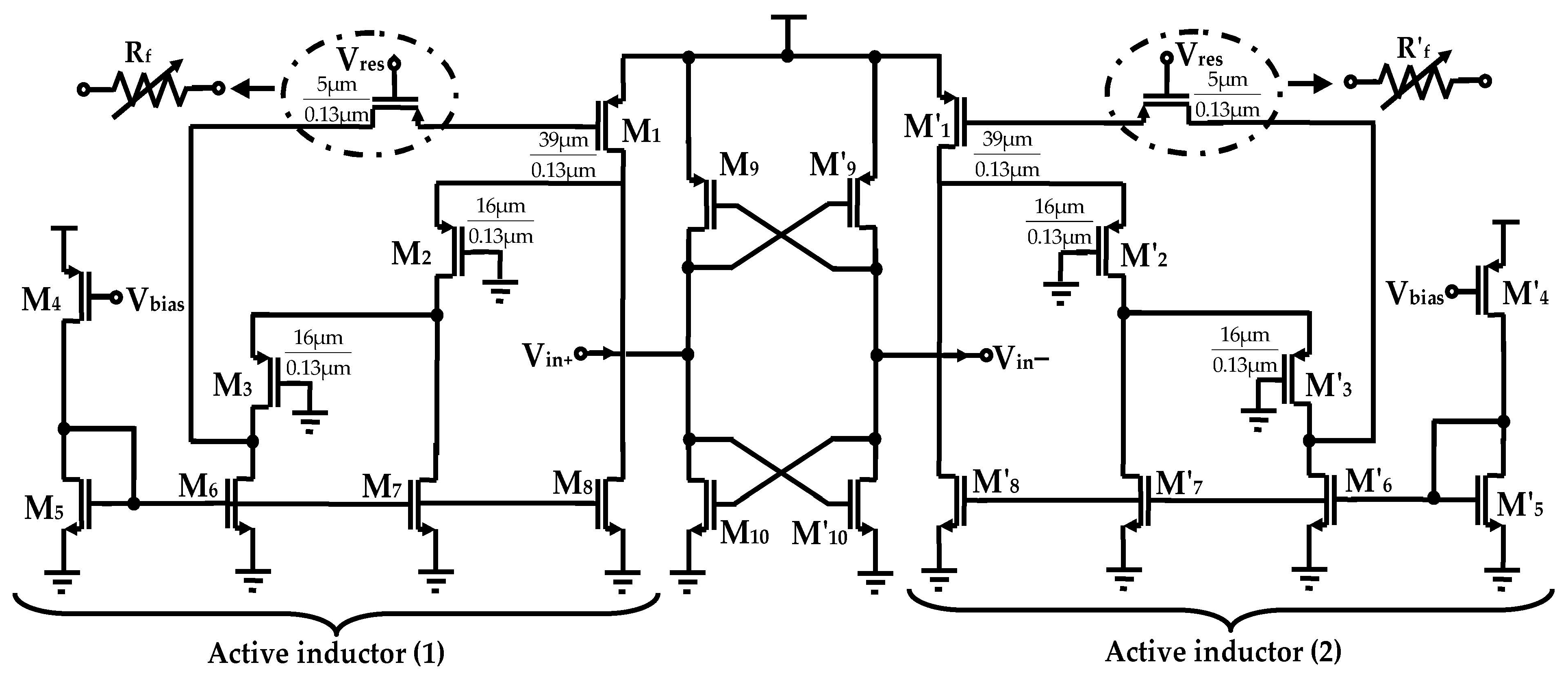
2.2. Implementation of the Proposed Differential Active Inductor
3. Proposed Tunable Bandpass Filter
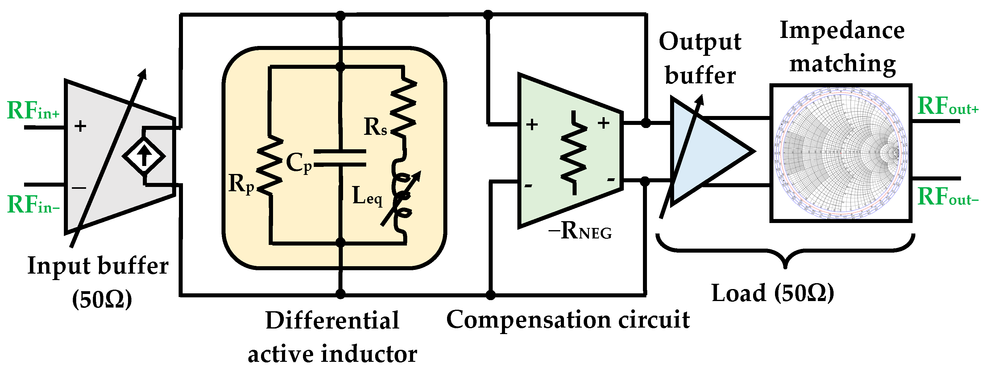
3.1. Bandpass Filter Design Methodology
3.2. Theoretical Analysis
4. Simulation Results and Discussion
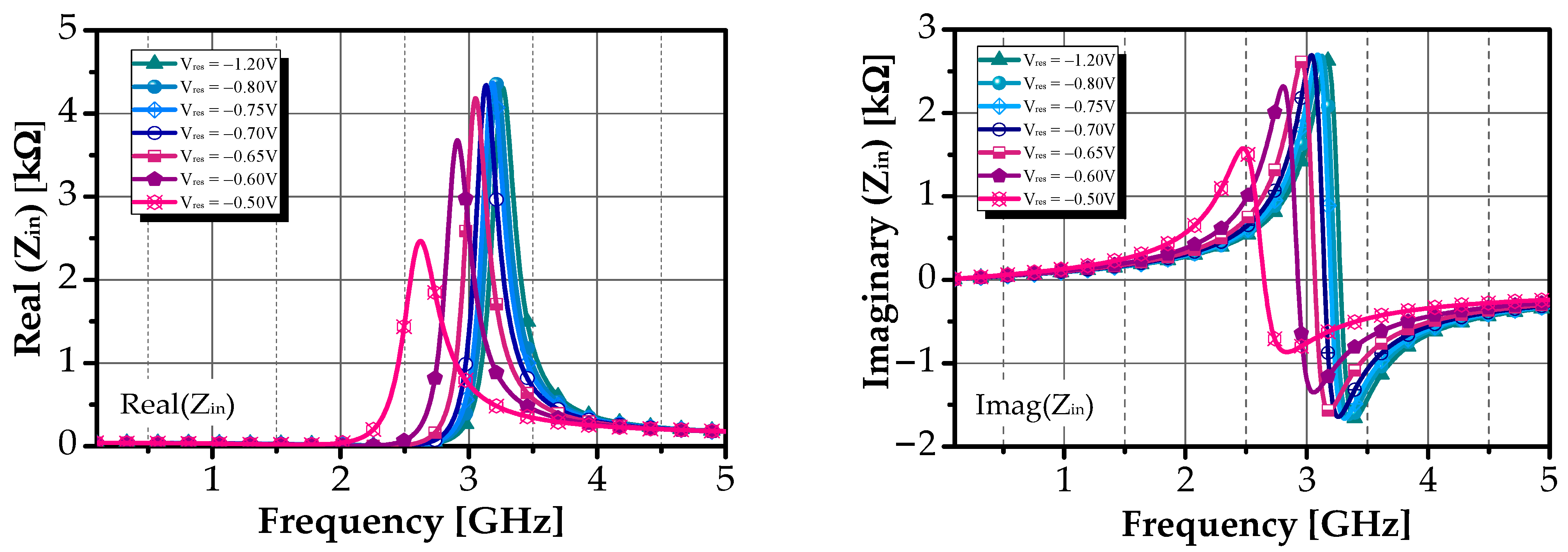
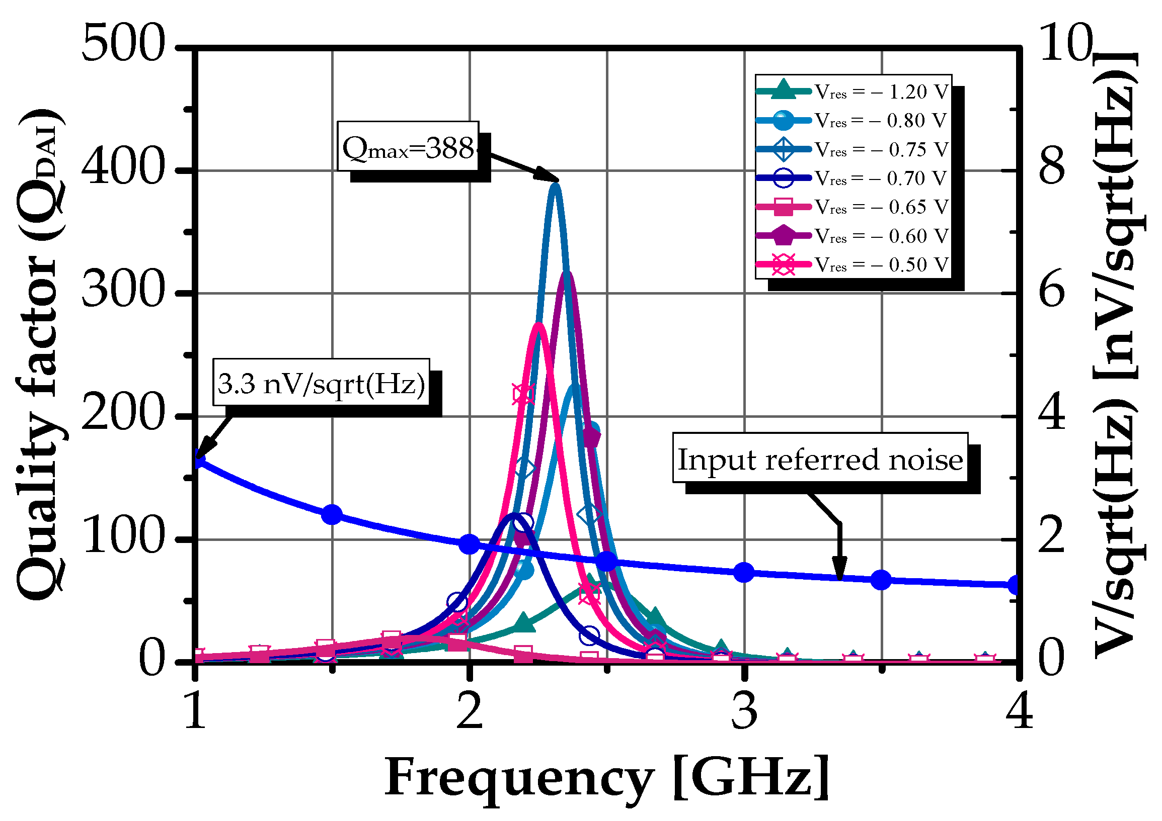
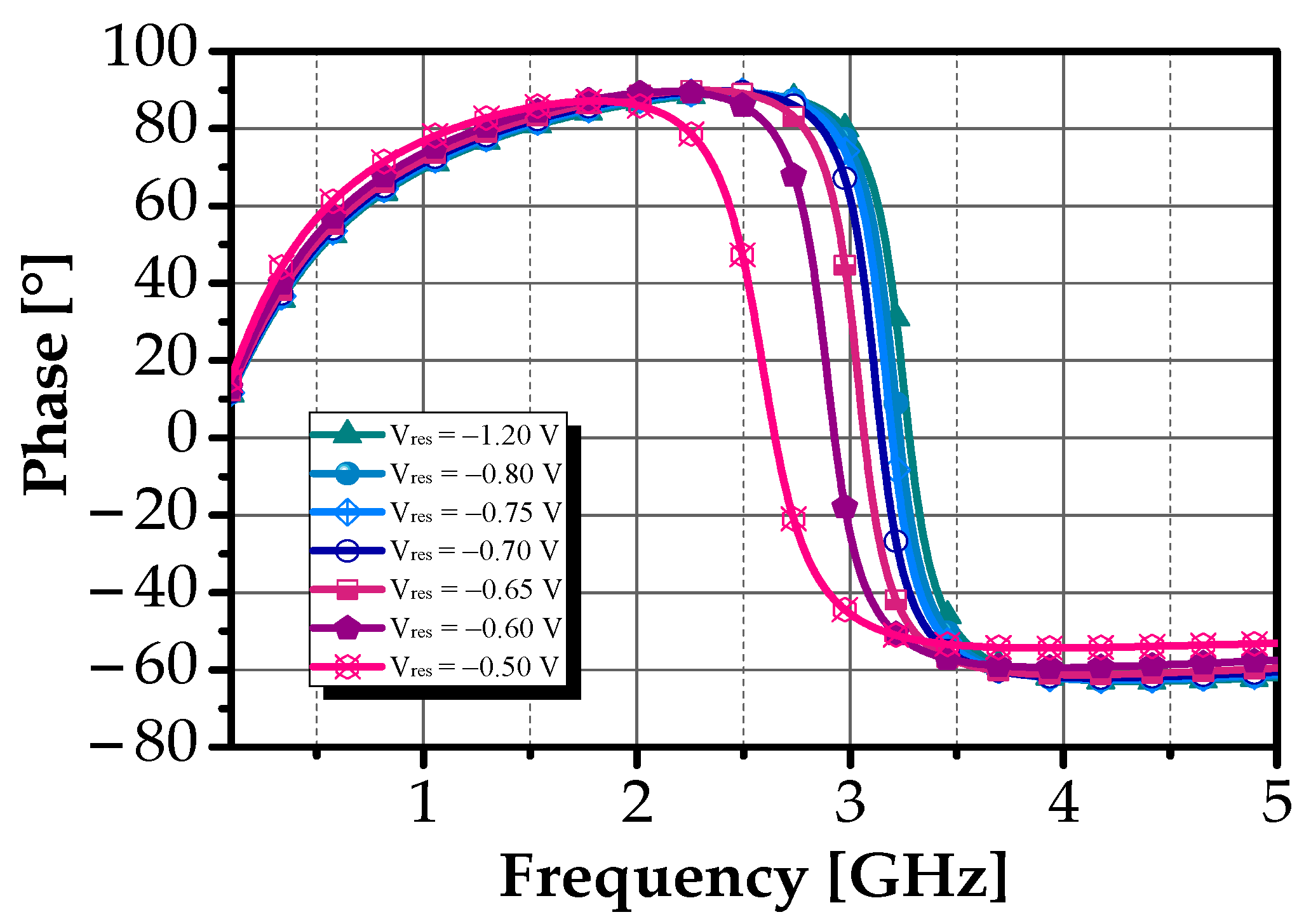
4.1. Differential Active Inductor Performances
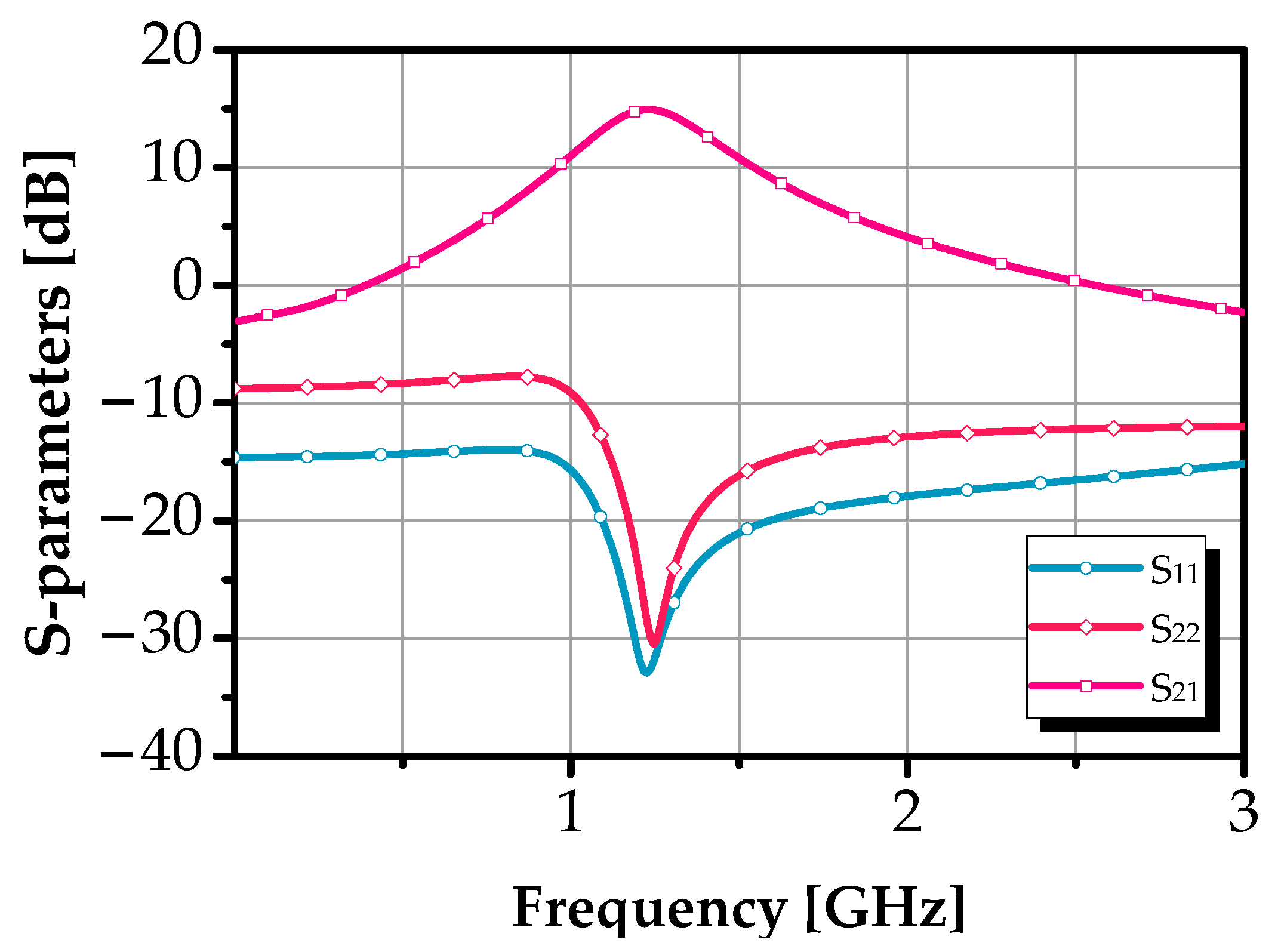
4.2. Bandpass Filter Performances
4.3. Monte Carlo Analysis
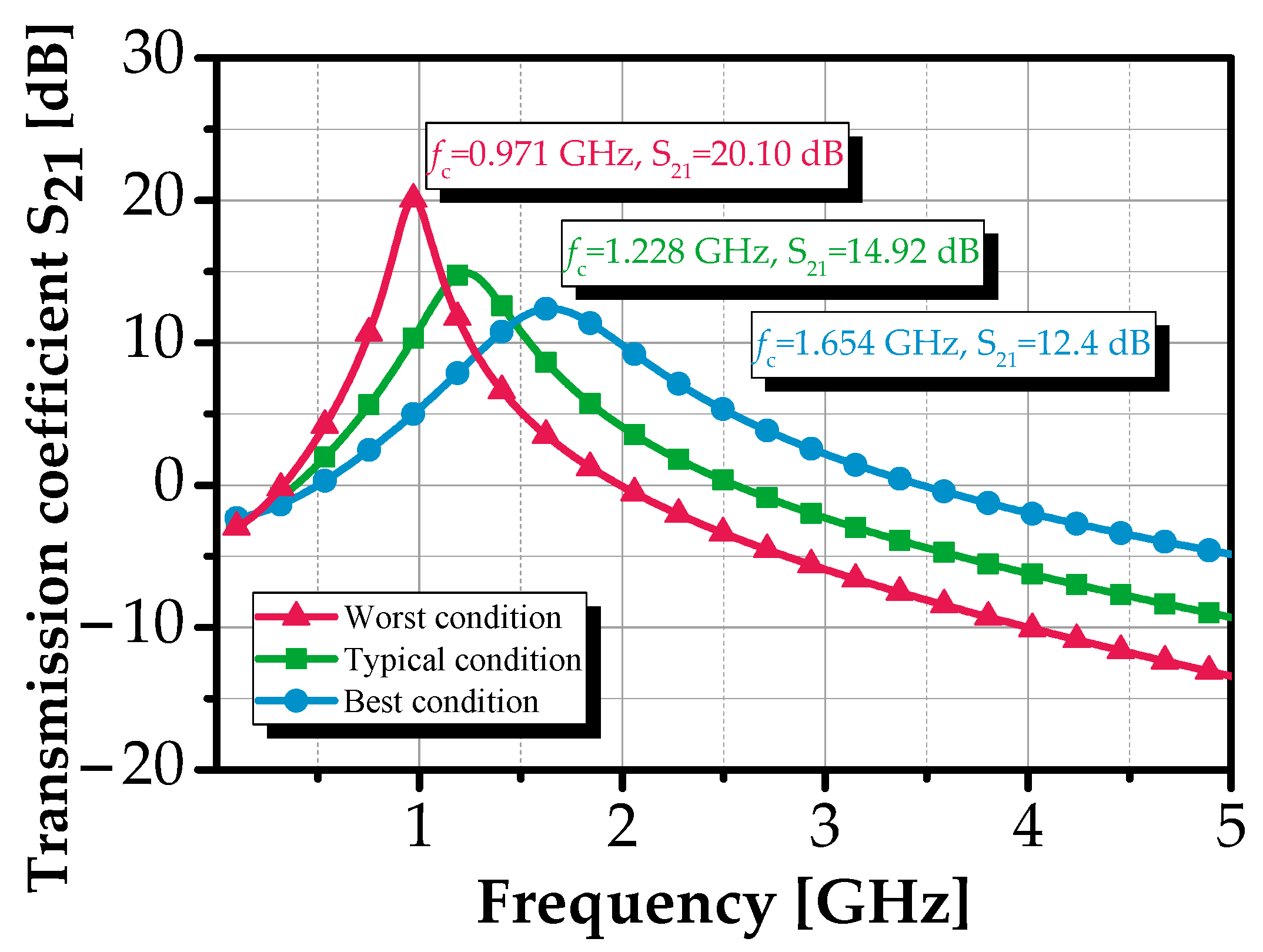
4.4. Process Corner Analysis
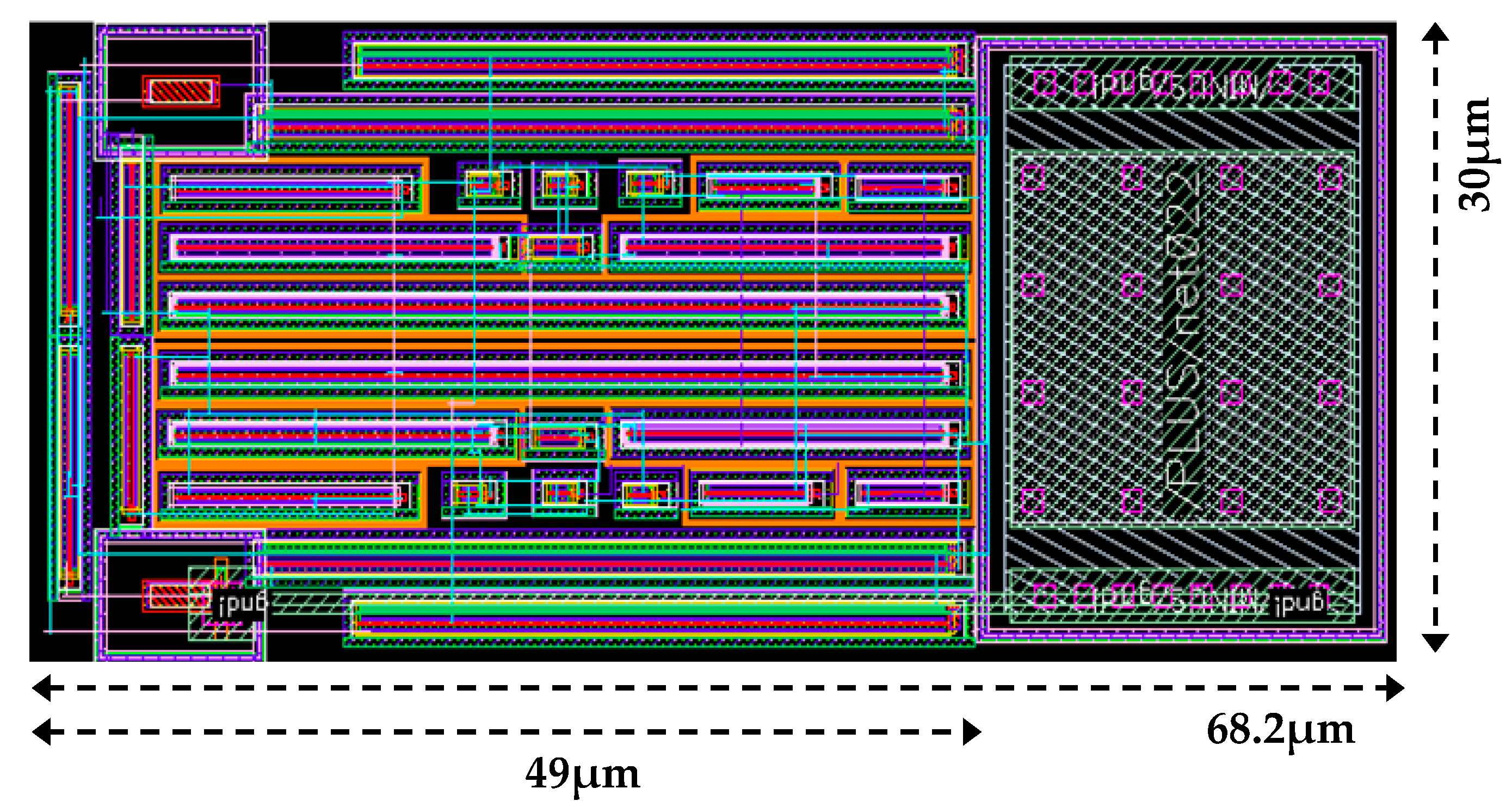
4.5. Layout and Performance Comparison

| Reference | [39] | [55] | [56] | [57] | [58] | [59] | Our Work | |
|---|---|---|---|---|---|---|---|---|
| Parameter | ||||||||
| Filter order (N) | 2 | 2 | 2 | 2 | 2 | 1 | 2 | |
| Inductor Topology | Gyrator-C active inductor | |||||||
| SRF (GHz) | 1.16–3.27 | 5.15–5.35 | 1.6–2.9 | 1–2 | 3.02–3.76 | 0.1–1.3 | 0.28–2.426 | |
| −3dB BW (MHz) | 65 | 15 | 80 | 1000 | - | 300 | 294–406 | |
| VDD (V) | 1.0 | 1.2 | 1.8 | 1.2 | 20 | - | 1.2 | |
| Inductor Q | 300–794 | 964 | - | - | 12 | - | 388 | |
| Gain S21 (dB) | 26.62–33.45 | 15 | 5.75 | 0.5 | −12.2–13.7 | 0 | 8.89–16.54 | |
| PDC (mW) | 4.04–6.44 | 7.71 | 6 | 30 | 506 | 120 | 14.1–20.3 | |
| P1dB (dBm) | 2.72 | −2.8 | −7 | −21 | −11.65 | 5 | −3.78 | |
| NF (dB) | 14.48–16.56 | 21.7 | 6 | 19 | N/A | 11 | 18.41–24.60 | |
| DR (dB-Hz) | 161.7 a | 149.5 a | 161 a | 134 a | - | 82 | 151.8 | |
| FoM1 (dB-Hz/mW) | 153.9 a | 140.6 a | 153.1 a | 119.2 a | - | 61.2 a | 140.3 | |
| FoM2 (dB) | 92.7 a | 92.2 | 91 a | 41.8 a | - | 64 a | 73 | |
| Area (mm2) | 0.017 | - | 0.023 | 0.18 | 0.062 | - | 0.002 b | |
| Sim./Meas. | Sim. | Sim. | Sim. | Meas. | Meas. | Meas. | Sim. | |
| Process Technology | 130 nm CMOS | 40 nm CMOS | 180 nm CMOS | 130 nm CMOS | 0.5 µm pHEMT GaN | N/A | 130 nm CMOS | |
5. Conclusions
Author Contributions
Funding
Institutional Review Board Statement
Informed Consent Statement
Data Availability Statement
Acknowledgments
Conflicts of Interest
Abbreviations
| BPF | Bandpass Filter |
| DAI | Differential Active Inductor |
| UHF | Ultra-High Frequency |
| CS | Common Source |
| CMOS | Complementary metal-oxide-semiconductor |
| IIP3 | Third-Order Input Intercept Point (IIP3) |
| DC | Direct Current |
| RF | Radio Frequency |
| IoT | Internet of Things |
| MTC | Machine-Type Communication |
| ISM | Industrial, Scientific, and Medical |
| Wi-Fi | Wireless Fidelity |
| BAN | Body Area Network |
| HART | Highway Addressable Remote Transducer |
| ZigBee | Zonal Intercommunication Global Standard |
| LPWAN | Low-Power Wide Area Networks |
| WSN | Wireless Sensor Network |
| GNSS | Global Navigation Satellite System |
| IC | Integrated Circuit |
| LNA | Low-Noise Amplifier |
| LPF | Low Pass Filter |
| VGA | Variable Gain Amplifier |
| DAC | Digital Analog Converter |
| ADC | Analog Digital Converter |
| PD | Phase Detector |
| CP | Charge Pump |
| VCO | Voltage Controlled Oscillator |
| FD | Frequency Divider |
| MOSFET | Metal-Oxide-Semiconductor Field-Effect Transistor |
| GBWP | Gain-Bandwidth Product |
| Op-Amps | Operational Amplifiers |
| DTT | Digital Terrestrial Television |
| LTE | Long-Term Evolution |
| GSM | Global System for Mobile communication |
| LoRa | Long Range Wide Area |
| PVT | Process Voltage Temperature |
| OTA | Operational Transconductance Amplifier |
| SRF | Self-Resonant Frequency |
| MIM | Metal Insulator Metal |
| GBW | Gain Bandwidth |
| PSS | Periodic Steady State |
| IIP3 | Input Third-Order Intercept Point |
| BW | Bandwidth |
| NF | Noise Figure |
| OTV | Oxide Thickness Variation |
| WKF | Metal Gate Work Function Fluctuations |
| RDF | Random Dopant Fluctuations |
| LWR | Line-Width Roughness |
| DR | Dynamic Range |
| FoM | Figure of Merit |
References
- ITU. Utility Radio Communications Operating in the Land-Mobile Service; ITU: Geneva, Switzerland, 2018. [Google Scholar]
- Aragón-Zavala, A.; Angueira, P.; Montalban, J.; Vargas-Rosales, C. Radio propagation in terrestrial broadcasting television systems: A comprehensive survey. IEEE Access 2021, 9, 34789–34817. [Google Scholar] [CrossRef]
- Więcek, D.; Mora, M.; Michalski, I. Coexistence of 5G/6G and Digital Terrestrial Television Networks. Appl. Sci. 2024, 14, 5756. [Google Scholar] [CrossRef]
- Graham, A.; Kirkman, N.C.; Paul, P.M. Mobile Radio Network Design in the VHF and UHF Bands: A Practical Approach, 1st ed.; John Wiley & Sons: Hoboken, NJ, USA, 2007. [Google Scholar]
- Quintana-Diaz, G.; Nodar-Lopez, D.; Muíño, A.G.; Agelet, F.A.; Cappelletti, C.; Ekman, T. Detection of radio interference in the UHF amateur radio band with the Serpens satellite. Adv. Space Res. 2022, 69, 1159–1169. [Google Scholar] [CrossRef]
- Xu, Z.; Liu, J.; Zhang, W.; Zhou, S.; Waug, W. Capacity analysis and comparison for cellular systems over different frequency bands. In Proceedings of the IEEE International Conference on Network Infrastructure and Digital Content (IC-NIDC), Beijing, China, 23–25 September 2016; pp. 135–138. [Google Scholar]
- Mekki, K.; Bajic, E.; Chaxel, F.; Meyer, F. Overview of cellular LPWAN technologies for IoT deployment: Sigfox, LoRaWAN, and NB-IoT. In Proceedings of the IEEE International Conference on Pervasive Computing and Communications Workshops (Percom Workshops), Athens, Greece, 19–23 March 2018; pp. 197–202. [Google Scholar]
- Al-Yasir, Y.I.A.; Ojaroudi Parchin, N.; Abd-Alhameed, R.A.; Abdulkhaleq, A.M.; Noras, J.M. Recent Progress in the Design of 4G/5G Reconfigurable Filters. Electronics 2019, 8, 114. [Google Scholar] [CrossRef]
- Banu, M.; Tsividis, Y. The MOSFET-C technique. In Design of High Frequency Integrated Analogue Filters, 1st ed.; Sun, Y., Ed.; Series 14; The Institution of Engineering and Technology: London, UK, 2007; pp. 35–56. [Google Scholar]
- Banu, M.; Tsividis, Y. Fully integrated active RC filters in MOS technology. IEEE J. Solid-State Circuits 1983, 18, 644–651. [Google Scholar] [CrossRef]
- Chen, W.-K. Passive, Active, and Digital Filters, 1st ed.; CRC Press: Boca Raton, FL, USA, 2005; Chapter 17. [Google Scholar]
- Mohan, P.A. VLSI Analog Filters: Active RC, OTA-C, and SC, 2nd ed.; Springer Science & Business Media: New York, NY, USA, 2012; pp. 251–432. [Google Scholar]
- Sun, Y. (Ed.) Architectures and design of OTA/gm-C filters. In Design of High Frequency Integrated Analogue Filters, 1st ed.; Series 14; The Institution of Engineering and Technology: London, UK, 2007; pp. 1–34. [Google Scholar]
- Li, D.; Tsividis, Y. Active LC filters on silicon. IEE Proc.-Circuits Devices Syst. 2000, 147, 49–56. [Google Scholar] [CrossRef]
- Dandan, L.; Yannis, T. Active filters using integrated inductors. In Design of High Frequency Integrated Analogue Filters, 1st ed.; Sun, Y., Ed.; Series 14; The Institution of Engineering and Technology: London, UK, 2007; pp. 57–80. [Google Scholar]
- Bahl, I.J. High-performance inductors. IEEE Trans. Microw. Theory Tech. 2001, 49, 654–664. [Google Scholar] [CrossRef]
- Mathúna, C.Ó.; Wang, N.; Kulkarni, S.; Roy, S. Review of integrated magnetics for power supply on chip (PwrSoC). IEEE Trans. Power Electron. 2012, 27, 4799–4816. [Google Scholar] [CrossRef]
- Burghartz, J.; Edelstein, D.; Jenkins, K.; Jahnes, C.; Uzoh, C.; O’Sullivan, E.; Chan, K.; Soyuer, M.; Roper, P.; Cordes, S. Monolithic spiral inductors fabricated using a VLSI Cu-damascene interconnect technology and low-loss substrates. In Proceedings of the International Electron Devices Meeting, Technical Digest. San Francisco, CA, USA, 8–11 December 1996; pp. 99–102. [Google Scholar]
- Yeşil, A.; Kaçar, F.; Gürkan, K. Lossless grounded inductance simulator employing single VDBA and its experimental band-pass filter application. AEU Int. J. Electron. Commun. 2014, 68, 143–150. [Google Scholar] [CrossRef]
- Kacar, F.; Kuntman, H. CFOA-based lossless and lossy inductance simulators. Radioengineering 2011, 20, 627–631. [Google Scholar]
- Kumar, N.; Vista, J.; Ranjan, A. A tuneable active inductor employing DXCCTA: Grounded and floating operation. Microelectron. J. 2019, 90, 1–11. [Google Scholar] [CrossRef]
- Senani, R.; Bhaskar, D.R.; Singh, A.K. Current Conveyors: Variants, Applications and Hardware Implementations; Springer: Cham, Switzerland, 2015; pp. 469–497. [Google Scholar]
- Yuan, F. CMOS Active Inductors and Transformers: Principle, Implementation and Applications, 1st ed.; Springer: New York, NY, USA, 2008. [Google Scholar]
- Wang, X.; Zhang, W.; Na, W.; Jin, D.; Xie, H.; Ren, Y.; Li, N.; Gao, W.; Wu, Y. A novel CMOS active inductor with high quality factor, high linearity and mutually independent tuning of inductance and quality factor. Microelectron. J. 2023, 141, 105984. [Google Scholar] [CrossRef]
- Momen, H.G.; Yazgi, M.; Kopru, R. A low loss, low voltage and high Q active inductor with multi-regulated cascade stage for RF applications. In Proceedings of the IEEE International Conference on Electronics, Circuits, and Systems (ICECS), Cairo, Egypt, 6–9 December 2015; pp. 149–152. [Google Scholar]
- Gardeshkhah, R.; Saatlo, A.N. A New Tunable Gyrator-C-Based Active Inductor Circuit for Low Power Applications. J. Circuits Syst. Comput. 2023, 32, 2350235. [Google Scholar] [CrossRef]
- Lai, Q.-T.; Mao, J.-F. A new floating active inductor using resistive Feedback Technique. In Proceedings of the IEEE MTT-S International Microwave Symposium, Anaheim, CA, USA, 23–28 May 2010; pp. 1748–1751. [Google Scholar]
- Faruqe, O.; Amin, M.T. Active inductor with feedback resistor based voltage controlled oscillator design for wireless applications. Int. J. Electron. Telecommun. 2019, 65, 57–64. [Google Scholar] [CrossRef]
- Saberkari, A.; Ziabakhsh, S.; Martinez, H.; Alarcon, E. Design and comparison of flipped active inductors with high quality factors. Electron. Lett. 2014, 50, 925–927. [Google Scholar] [CrossRef]
- Nediyara Suresh, L.; Manickam, B. Multiple cascode flipped active inductor-based tunable bandpass filter for fully integrated RF front-end. IET Circuits Devices Syst. 2020, 14, 93–99. [Google Scholar] [CrossRef]
- Farahani, M.M.; Mazloum, J.; Fouladian, M. An ultra-wideband low noise amplifier with cascaded flipped-active inductor for cognitive radio applications. Integration 2023, 93, 102046. [Google Scholar] [CrossRef]
- Jeong, Y.J.; Kim, Y.M.; Chang, H.J. Low-power CMOS VCO with a low-current, high-Q active inductor. IET Microw. Antennas Propag. 2012, 6, 788–792. [Google Scholar] [CrossRef]
- Sackinger, E.; Fischer, W.C. A 3-GHz 32-dB CMOS limiting amplifier for SONET OC-48 receivers. IEEE J. Solid-State Circuits 2000, 35, 1884–1888. [Google Scholar] [CrossRef]
- Yodprasit, U.; Ngarmnil, J. Q-enhancing technique for rf CMOS active inductor. In Proceedings of the IEEE International Symposium on Circuits and Systems (ISCAS), Geneva, Switzerland, 28–31 May 2000; pp. 589–592. [Google Scholar]
- Sato, T.; Ito, T. Design of low distortion active inductor and its applications. Analog Integr. Circuits Signal Process. 2013, 75, 245–255. [Google Scholar] [CrossRef]
- Pantoli, L.; Stornelli, V.; Leuzzi, G. Class AB gyrator-based active inductor. In Proceedings of the Integrated Nonlinear Microwave and Millimetre-Wave Circuits Workshop (INMMiC), Taormina, Italy, 1–2 October 2015; pp. 1–3. [Google Scholar]
- Thanachayanont, A.; Sae Ngow, S. Class AB VHF CMOS active inductor. In Proceedings of the 45th Midwest Symposium on Circuits and Systems (MWSCAS), Tulsa, OK, USA, 4–7 August 2002; p. I-64. [Google Scholar]
- Gorjizad, Z.; Shojaee, A.; Abrishamifar, A. A compact and tunable active inductor-based bandpass filter with high quality factor for Wireless LAN applications. AEU Int. J. Electron. Commun. 2024, 187, 155540. [Google Scholar] [CrossRef]
- Ben Hammadi, A.; Haddad, F.; Mhiri, M.; Saad, S.; Besbes, K. RF and microwave reconfigurable bandpass filter design using optimized active inductor circuit. Int. J. RF Microw. Comput.-Aided Eng. 2018, 28, e21550. [Google Scholar] [CrossRef]
- Saad, S.; Mhiri, M.; Hammadi, A.B.; Besbes, K. A new low-power, high-Q, wide tunable CMOS active inductor for RF applications. IETE J. Res. 2016, 62, 265–273. [Google Scholar] [CrossRef]
- Saad, S.; Haddad, F.; Hammadi, A.B. Impact of multi-finger MOSFET geometry on the electrical performance of RF circuits. Microelectron. Reliab. 2022, 129, 114445. [Google Scholar] [CrossRef]
- Ho, C.C.; Kuo, C.W.; Chan, Y.J.; Lien, W.Y.; Guo, J.C. 0.13-µm RF CMOS and varactors performance optimization by multiple gate layouts. IEEE Trans. Electron Devices 2004, 51, 2181–2185. [Google Scholar] [CrossRef]
- Yeh, K.L.; Guo, J.C. Narrow-width effect on high-frequency performance and RF noise of sub-40-nm multifinger nMOSFETs and pMOSFETs. IEEE Trans. Electron Devices 2012, 60, 109–116. [Google Scholar]
- Ler, C.L.; bin A’ain, A.K.; Kordesch, A.V. Compact, High-Q, and Low-Current Dissipation CMOS Differential Active Inductor. IEEE Microw. Wirel. Compon. Lett. 2008, 18, 683–685. [Google Scholar] [CrossRef]
- Ler, C.L.; A’ain, A.K.B.; Kordesch, A.V. CMOS active inductor linearity improvement using feed-forward current source technique. IEEE Trans. Microw. Theory Tech. 2009, 57, 1915–1924. [Google Scholar] [CrossRef]
- Li, C.; Gong, F.; Wang, P. Analysis and design of a high-Q differential active inductor with wide tuning range. IET Circuits Devices Syst. 2010, 4, 486–495. [Google Scholar] [CrossRef]
- Mehra, R.; Kumar, V.; Islam, A. Reliable and Q-Enhanced Floating Active Inductors and Their Application in RF Bandpass Filters. IEEE Access 2018, 6, 48181–48194. [Google Scholar] [CrossRef]
- Kumar, V.; Mehra, R.; Islam, A. A 2.5 GHz Low Power, High-Q, Reliable Design of Active Bandpass Filter. IEEE Trans. Device Mater. Reliab. 2017, 17, 229–244. [Google Scholar] [CrossRef]
- Li, Y.; Hwang, C.H.; Li, T.Y.; Han, M.H. Process-variation effect, metal-gate work-function fluctuation, and random-dopant fluctuation in emerging CMOS technologies. IEEE Trans. Electron Devices 2009, 57, 437–447. [Google Scholar] [CrossRef]
- Saha, S.K. Compact MOSFET modeling for process variability-aware VLSI circuit design. IEEE Access 2014, 2, 104–115. [Google Scholar] [CrossRef]
- Sundarasaradula, Y.; Thanachayanont, A. A 1-V, 6-nW programmable 4th-order bandpass filter for biomedical applications. Analog Integr. Circuits Signal Process. 2016, 89, 89–98. [Google Scholar] [CrossRef]
- He, X.; Kuhn, W.B. A fully integrated Q-enhanced LC filter with 6 dB noise figure at 2.5 GHz in SOI. In Proceedings of the IEE Radio Frequency Integrated Circuits (RFIC) Systems, Digest of Papers. Fort Worth, TX, USA, 6–8 June 2004; pp. 643–646. [Google Scholar]
- Christensen, K.T.; Lee, T.H.; Bruun, E. A high dynamic range programmable CMOS front-end filter with a tuning range from 1850 to 2400 MHz. Analog Integr. Circuits Signal Process. 2005, 42, 55–64. [Google Scholar] [CrossRef]
- Gao, Z.; Ma, J.; Yu, M.; Ye, Y. A fully integrated CMOS active bandpass filter for multiband RF front-ends. IEEE Trans. Circuits Syst. II Express Br. 2008, 55, 718–722. [Google Scholar]
- Yadav, P.K.; Misra, P.K. Tunable bandpass filter using double resistive feedback floating active inductor for 5 GHz wireless LAN Applications. Analog Integr. Circuits Signal Process. 2021, 108, 205–213. [Google Scholar] [CrossRef]
- Hu, F.; Mouthaan, K. L-band bandpass filter with high out-of-band rejection based on CMOS active series and shunt inductors. In Proceedings of the IEEE MTT-S International Microwave Symposium, Tampa, FL, USA, 1–6 June 2014; pp. 1–3. [Google Scholar]
- Suresh, L.N.; Manickam, B. Design and application of CMOS active inductor in bandpass filter and VCO for reconfigurable RF front-end. Integration 2022, 82, 115–126. [Google Scholar] [CrossRef]
- Herbert, T.B.; Hyland, J.S.; Abdullah, S.; Wight, J.; Amaya, R.E. An active bandpass filter for LTE/WLAN applications using robust active inductors in gallium nitride. IEEE Trans. Circuits Syst. II Express Br. 2021, 68, 2252–2256. [Google Scholar] [CrossRef]
- Leuzzi, G.; Stornelli, V.; Del Re, S. A tuneable active inductor with high dynamic range for band-pass filter applications. IEEE Trans. Circuits Syst. II Express Br. 2011, 58, 647–651. [Google Scholar] [CrossRef]


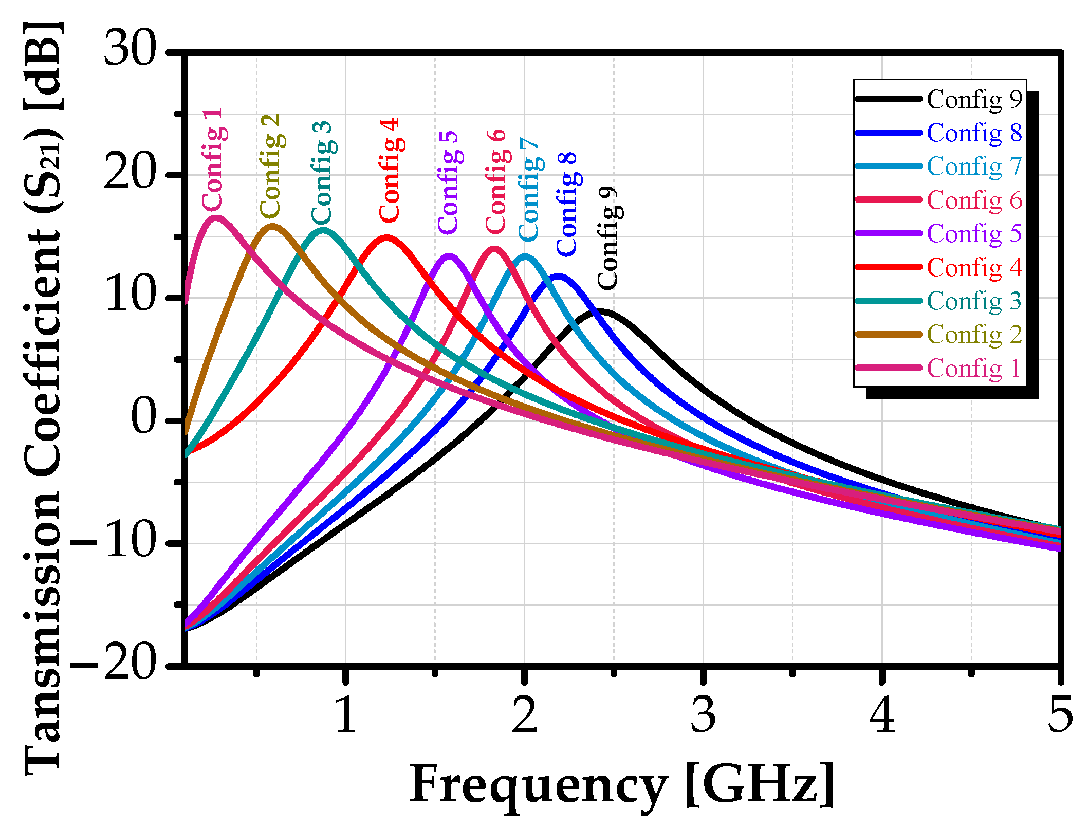
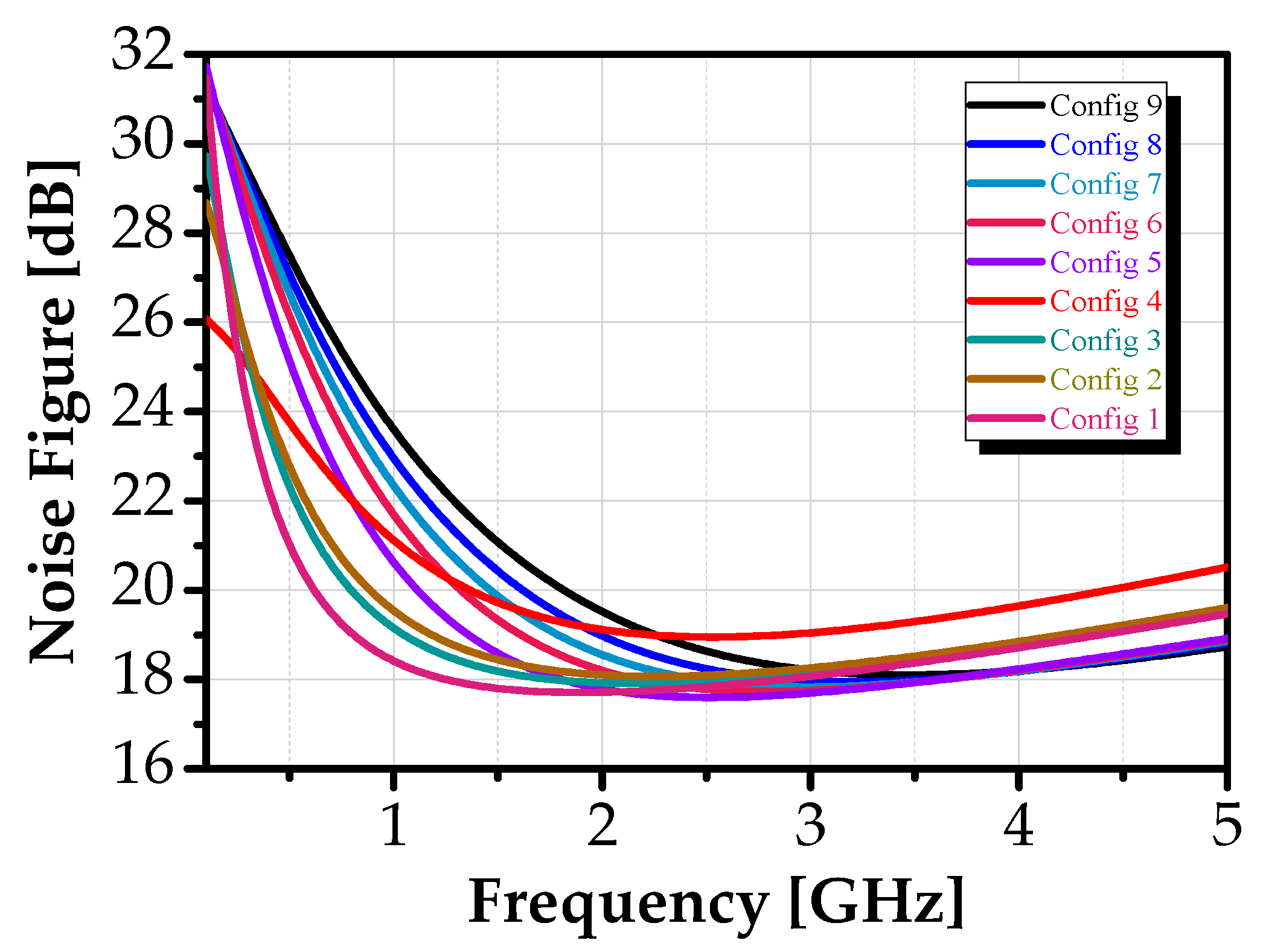

| Config | Vres (mV) | Vbias2 (mV) | fc (GHz) | S21 (dB) | BW (MHz) | QBPF | NF (dB) | PDC (mW) |
|---|---|---|---|---|---|---|---|---|
| 1 | 200 | 600 | 0.28 | 16.54 | 321 | 0.9 | 24.60 | 15.2 |
| 2 | 130 | 600 | 0.59 | 15.84 | 357 | 1.7 | 21.86 | 15.2 |
| 3 | 100 | 580 | 0.87 | 15.52 | 370 | 2.35 | 19.63 | 14.9 |
| 4 | 100 | 500 | 1.22 | 14.92 | 406 | 3 | 20.19 | 14.1 |
| 5 | −200 | 800 | 1.57 | 13.42 | 297 | 5.3 | 18.41 | 20.3 |
| 6 | −250 | 800 | 1.83 | 14.02 | 287 | 6.4 | 18.48 | 20.3 |
| 7 | −300 | 800 | 2 | 13.38 | 318 | 6.29 | 18.55 | 20.3 |
| 8 | −400 | 800 | 2.19 | 11.78 | 397 | 5.52 | 18.63 | 20.3 |
| 9 | −1200 | 800 | 2.426 | 8.89 | 593 | 4.1 | 18.73 | 20.3 |
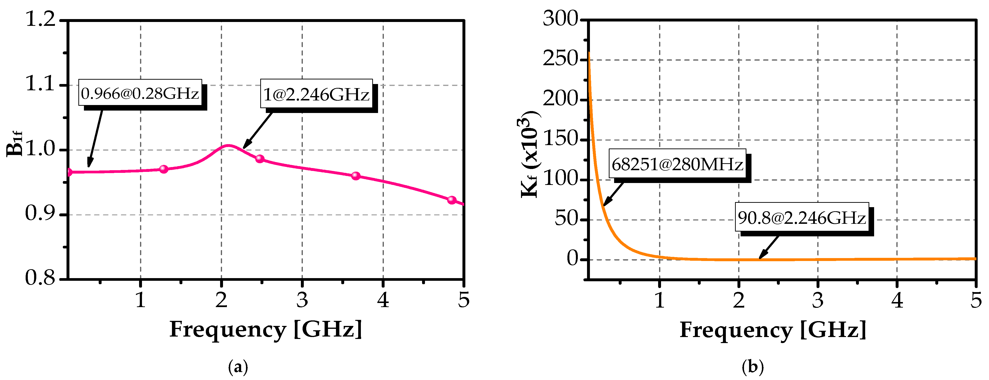
| Type | S21 (dB) | NF (dB) | Kf | B1f |
|---|---|---|---|---|
| Mean (µ) | 14.9 | 19.94 | 9.82 | 0.998 |
| Standard deviation (σ) | 0.345 | 0.379 | 0.484 | 0.000875 |
| Variability (σ/Mean) | 2.32% | 1.9% | 4.93% | 0.09% |
| Minimum (−3σ) | 13.67 | 19.81 | 8.6 | 0.997 |
| Maximum (+3σ) | 15.94 | 20.04 | 11.6 | 1.002 |
Disclaimer/Publisher’s Note: The statements, opinions and data contained in all publications are solely those of the individual author(s) and contributor(s) and not of MDPI and/or the editor(s). MDPI and/or the editor(s) disclaim responsibility for any injury to people or property resulting from any ideas, methods, instructions or products referred to in the content. |
© 2025 by the authors. Licensee MDPI, Basel, Switzerland. This article is an open access article distributed under the terms and conditions of the Creative Commons Attribution (CC BY) license (https://creativecommons.org/licenses/by/4.0/).
Share and Cite
Saad, S.; Haddad, F.; Ben Hammadi, A. A Compact and Tunable Active Inductor-Based Bandpass Filter with High Dynamic Range for UHF Band Applications. Sensors 2025, 25, 3089. https://doi.org/10.3390/s25103089
Saad S, Haddad F, Ben Hammadi A. A Compact and Tunable Active Inductor-Based Bandpass Filter with High Dynamic Range for UHF Band Applications. Sensors. 2025; 25(10):3089. https://doi.org/10.3390/s25103089
Chicago/Turabian StyleSaad, Sehmi, Fayrouz Haddad, and Aymen Ben Hammadi. 2025. "A Compact and Tunable Active Inductor-Based Bandpass Filter with High Dynamic Range for UHF Band Applications" Sensors 25, no. 10: 3089. https://doi.org/10.3390/s25103089
APA StyleSaad, S., Haddad, F., & Ben Hammadi, A. (2025). A Compact and Tunable Active Inductor-Based Bandpass Filter with High Dynamic Range for UHF Band Applications. Sensors, 25(10), 3089. https://doi.org/10.3390/s25103089