Article

Design and Realization of a High-Q Grounded Tunable Active Inductor for 5G NR (FR1) Transceiver Front-End Applications

1
Aix Marseille Université, Technopôle de Château Gombert, IM2NP UMR 7334, 13397 Marseille, France
2
Dynamics RF/mmW Consulting and Design, 39 Avenue du Vercors, 38600 Grenoble, France
*
Author to whom correspondence should be addressed.
Sensors 2025, 25(10), 3070; https://doi.org/10.3390/s25103070
Submission received: 3 April 2025 / Revised: 9 May 2025 / Accepted: 11 May 2025 / Published: 13 May 2025
(This article belongs to the Special Issue Feature Papers in Electronic Sensors 2025)

Abstract

:
This paper presents a wide-tuning-range, low-power tunable active inductor (AI) designed and fabricated using 130 nm CMOS technology with six metal layers. To achieve high performance with a relatively small silicon area and low power consumption, the AI structure is carefully designed and optimized using a cascode stage, a feedback resistor, and multi-gate finger transistors. In the proposed circuit topology, inductance tuning is realized by adjusting both the bias current and the feedback resistor. The performance of the circuit is evaluated in terms of tuning range, quality factor, power consumption, and chip area. The functionality of the fabricated device is experimentally validated, and the fundamental characteristics of the active inductor are measured over a wide frequency range using a Cascade GSG probe, with results compared to simulations. Experimental measurements show that, under a 1 V supply, the AI achieves a self-resonant frequency (SRF) of 3.961 GHz and a quality factor (Q) exceeding 1586 at 2.383 GHz. The inductance is tunable between 6.7 nH and 84.4 nH, with a total power consumption of approximately 2 mW. The total active area, including pads, is 345 × 400 µm2.

1. Introduction

The rapid evolution of 5G New Radio (NR) has significantly transformed wireless communication by enabling higher data rates, lower latency, and improved spectral efficiency. A key component of this advancement is Frequency Range 1 (FR1), spanning from 410 MHz to 7125 MHz, which serves as the backbone for early 5G deployment [1,2,3]. The FR1 spectrum offers notable advantages due to its favorable propagation characteristics, compatibility with existing cellular infrastructure, and support for multiple duplexing schemes, including Frequency Division Duplex (FDD) and Time Division Duplex (TDD) [4]. As wider bandwidths and higher operating frequencies become increasingly important, the design of high-performance RF front-end circuits faces new challenges, necessitating the development of compact, tunable, and power-efficient components.
Inductive elements are fundamental building blocks in RF front-end circuits, playing critical roles in applications such as low-noise amplifiers (LNAs), voltage-controlled oscillators (VCOs), impedance matching networks, and tunable filters. While passive spiral inductors have traditionally been favored for their simplicity, they present several drawbacks, including large silicon area requirements, limited tunability, and significant Q-factor degradation due to substrate losses [5]. These limitations become more pronounced at higher frequencies, making passive inductors less suitable for 5G NR (FR1) applications. To address these issues, recent research has increasingly focused on inductor-less architectures [6]. In this context, active inductors have emerged as promising alternatives, offering wide tunability, high inductance density, and improved integration with standard CMOS processes. However, practical deployment of active inductors is hindered by challenges such as low Q-factors, increased noise, and higher power consumption.
In the literature, a wide range of active inductance simulators has been proposed, classified based on their active/passive component configurations and whether they generate grounded or floating inductances. Examples include:
Current-feedback operational amplifiers (CFOAs) [7,8,9];
Current differencing transconductance amplifiers (CDTAs) [10];
Voltage differencing differential input-buffered amplifiers (VD-DIBAs) [11,12];
Differential voltage current conveyors (DVCCs) [13];
Differential current conveyors (DCCIIs) [14];
Fully differential current conveyors (FDCCIIs) [15];
Second-generation current conveyors (CCIIs) [16];
Third-generation current conveyors (CCIIIs) [17];
Differential difference current conveyors (DDCCs) [18,19,20];
Four-terminal floating nullors (FTFNs) [21];
Operational transconductance amplifiers (OTAs) [22,23], among others [24].
Among these, OTA-based active inductors, often implemented using gyrator-C topologies, have gained particular prominence due to their low transistor count, simplified architecture, and favorable high-frequency characteristics [23].
Several studies have proposed techniques to enhance the performance of gyrator-C-based active inductors. Negative resistance compensation [25] is one such method, improving the Q-factor by offsetting resistive losses using negative impedance converters (NICs) or cross-coupled transistors, without significant power overhead.
Another widely adopted approach is the cascode topology [26], which improves linearity, frequency response, and circuit stability by stacking transistors to increase output impedance, thus enhancing bandwidth and the Q-factor. Feedback-based techniques, including shunt and series feedback, are also employed to enhance inductance and the Q-factor while maintaining low power dissipation [27,28].
Additionally, advancements in fabrication technologies, such as FinFET [29], silicon-on-insulator (SOI) [30], and gallium nitride (GaN) [31], have reduced substrate losses and parasitic effects, further improving performance. Moreover, tunable biasing allows for dynamic adjustment of inductor characteristics, enabling adaptability to varying frequency and bandwidth requirements in 5G systems.
In this work, an active inductor circuit is proposed, offering a high quality factor and wide tunability, designed to meet the performance and efficiency demands of 5G NR (FR1) applications. Although many CMOS-based active inductor designs have been investigated, relatively few report measured results. This study introduces and experimentally characterizes a grounded CMOS active inductor based on a gyrator-C architecture.
The proposed design is optimized to operate within the sub-6 GHz FR1 spectrum, covering key frequency bands used in 5G. The focus is on addressing the core challenges of active inductor integration in 5G NR systems, with emphasis on achieving a high Q-factor, wide tunability, and low power consumption.
This paper is organized as follows: Section 2 reviews the fundamental principles of grounded gyrator-C active inductors and key design considerations. As well, it presents the proposed circuit topology and outlines the techniques employed to enhance its performance. Section 3 details the measurement results and performance analysis. Section 4 concludes the paper and discusses future research directions.

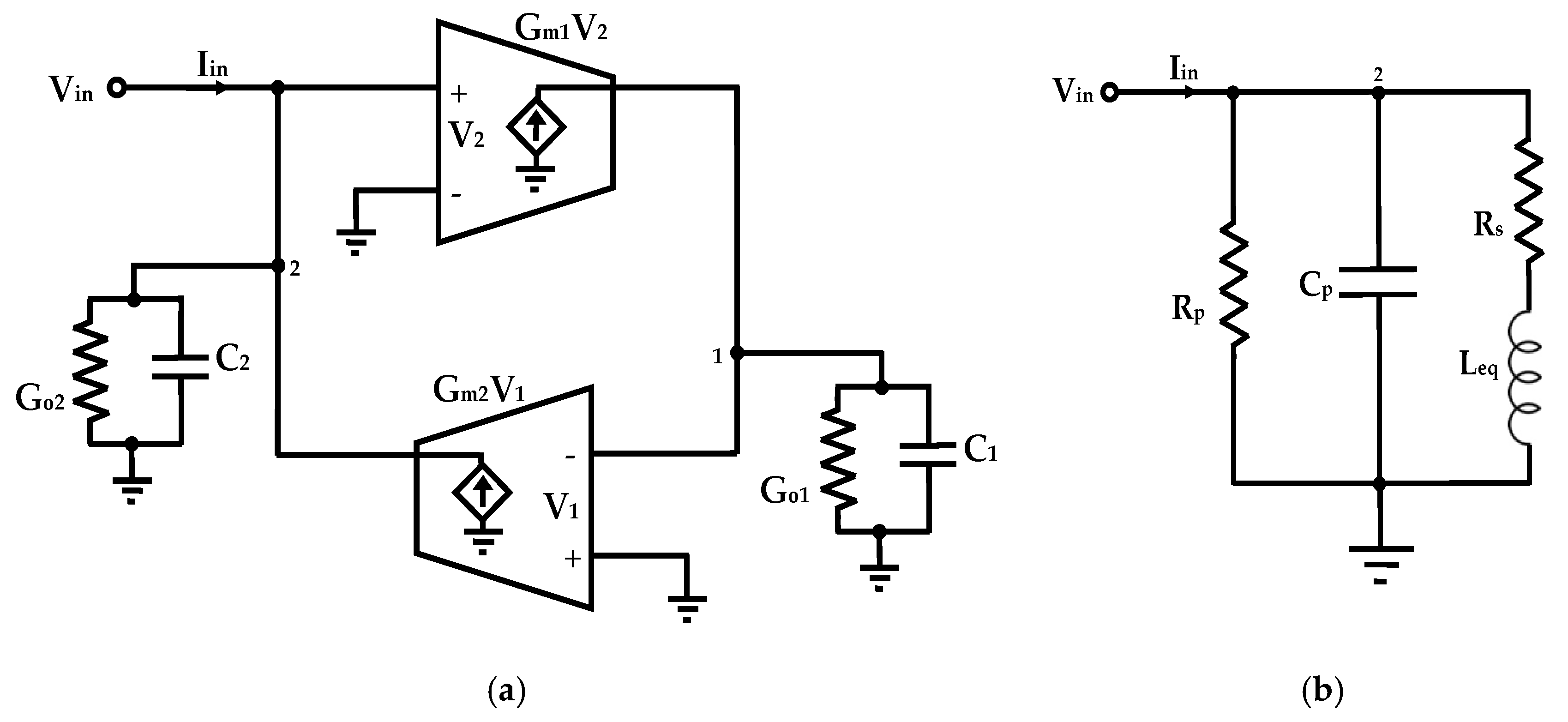
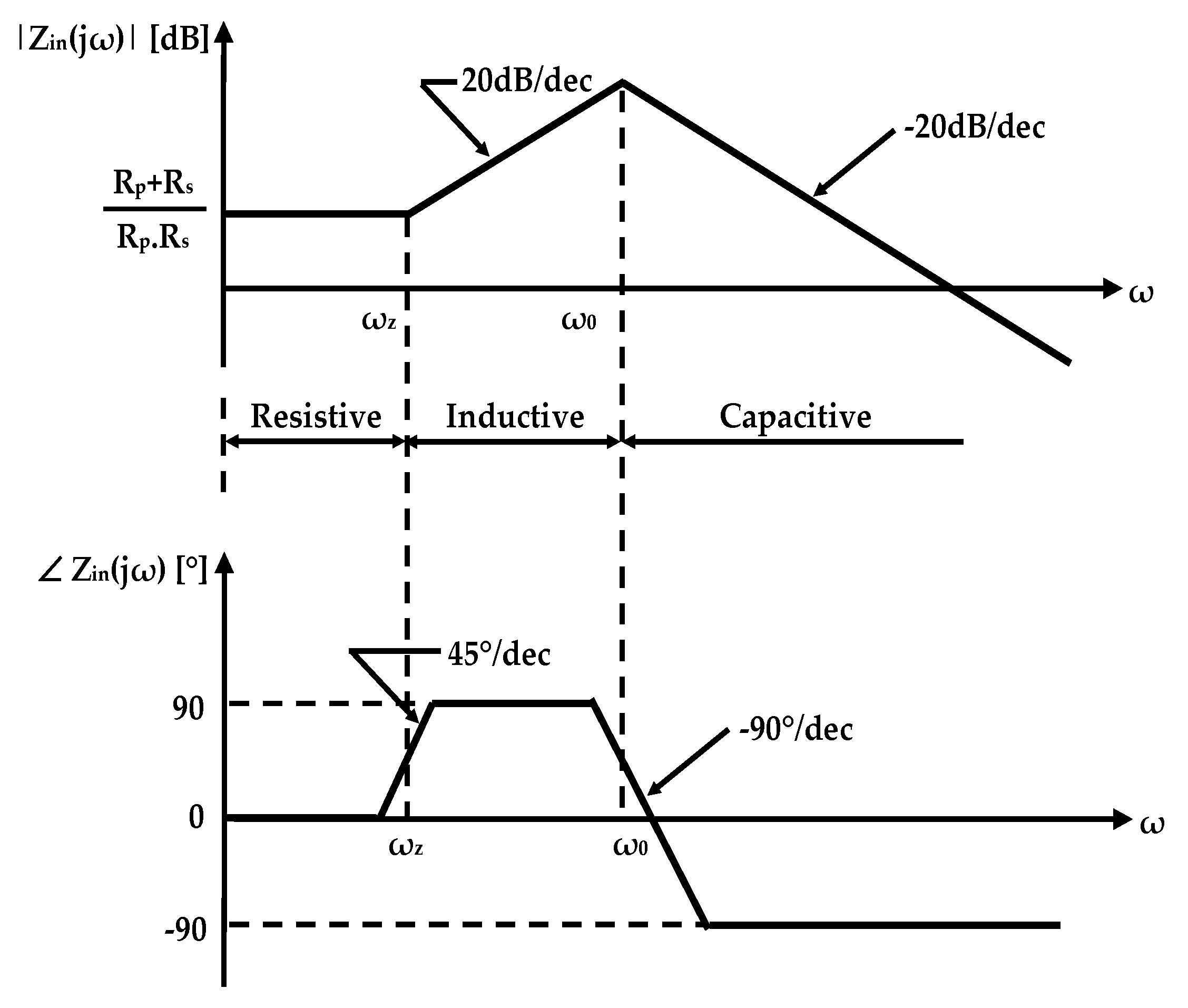
2. Grounded Gyrator-C-Based Tunable Active Inductor

2.1. Basic Concept

A gyrator can be realized by connecting two transconductors in series, where one exhibits positive transconductance and the other negative transconductance. When a capacitor is connected at the output, the resulting configuration forms a gyrator-C network, as illustrated in Figure 1a. By applying Kirchhoff’s Current Law (KCL) at nodes 1 and 2, the input admittance Yin can be derived:
Y in = I in V 2 = s C 2 + G o 2 + 1 s C 1 G m 1 G m 2 + G o 1 G m 1 G m 2
This expression reveals that the gyrator-C structure emulates the behavior of an equivalent RLC network, as represented in Figure 1b, with the corresponding parameters given by:
C p = C 2 ,   R p = 1 G o 2 ,   L e q = C 1 G m 1 G m 2 ,   and   R s = G o 1 G m 1 G m 2
where Go1 and Go2 denote the total input and output conductances of the transconductors at ports 1 and 2, respectively.
From Equation (2), a gyrator-C network can replicate the behavior of an inductor Leq along with its associated parasitic components: parallel resistance Rp, parallel capacitance Cp, and series resistance Rs. The equivalent inductance is directly proportional to the output capacitance C1 and inversely proportional to the transconductances Gm1 and Gm2, allowing for tunability through adjustment of these parameters. However, the inductive behavior is confined to a specific frequency range, which can be determined by analyzing the input impedance Zin, as defined in Equation (3).
Z in = R s L eq C p s L e q R s + 1 s 2 + s 1 R p C p + R s L e q + R s + R p R p L eq C p
The inductive behavior of a lossy gyrator-C network is limited to a frequency band bounded by the zero frequency ωz and the self-resonant frequency ω0. The self-resonant frequency ω0 is obtained by ensuring that the phase angle of Zin is zero, which occurs when the phase angles of the numerator and denominator are equal. By setting ∡ Zin(jω) = 0 and using s = jω, the value of ω0 can be derived as:
arctan 1 + s L eq R s = arctan R s + R p R p L eq C p ω 2 + s 1 R p C p + R s L eq
By solving Equation (4), ω0 can be expressed as:
ω 0 = 1 L eq C p R s L eq 2
From Equation (3), the input impedance Zin exhibits a zero at the frequency ωz = RS/Leq. Additionally, Zin has a pole corresponding to the resonant frequency given by ω p = ( R s + R p ) / R p L eq C p . Under the condition where Rp ≫ Rs and Rs is considered negligible, the resonant frequency ω0 and the pole frequency ωp can be approximated as nearly equal ω p = 1 / L eq C p ω 0 .
Figure 2 presents the Bode plots of Zin, illustrating the frequency-dependent behavior of the lossy gyrator-C network. The network demonstrates resistive characteristics at frequencies ω < ωz, behaves inductively in the range of ωz < ω < ω0, and exhibits capacitive behavior for ω > ω0 [23].
An additional key parameter of an active inductor is the quality factor Q, which quantifies its efficiency. For linear inductors, including active inductors, Q is defined as the ratio of the imaginary to the real part of the input impedance. Based on the transfer function of Zin in Equation (3), the quality factor for lossy active inductors can be expressed as:
Q = ω L eq R s 1 R s 2 C p / L eq ω 2 L eq C p 1 + R s / R p 1 + ω L eq / R s 2
Figure 3 shows the effect of variations in Rp and Rs on the quality factor of active inductors, using the parameter values Leq = 2.4 nH, Cp = 140 fF, Rs = 5 Ω, and Rp = 5 kΩ. Enhancement in the quality factor is achieved by increasing Rp and reducing Rs.
When the values of series and parallel resistances are comparable, the parallel resistance Rp has a more dominant influence on determining the quality factor Q. In advanced deep-submicron technologies, where the transconductance of transistors is significantly greater than their output conductance, the quality factor can be approximated by the following expression:
Q = R p ω L eq
Regardless of whether the circuit inherently exhibits a high Rp or achieves it through optimization techniques, the series resistance Rs remains the primary limiting factor affecting the quality factor. Therefore, the quality factor can also be estimated using the following expression:
Q = ω L eq R s

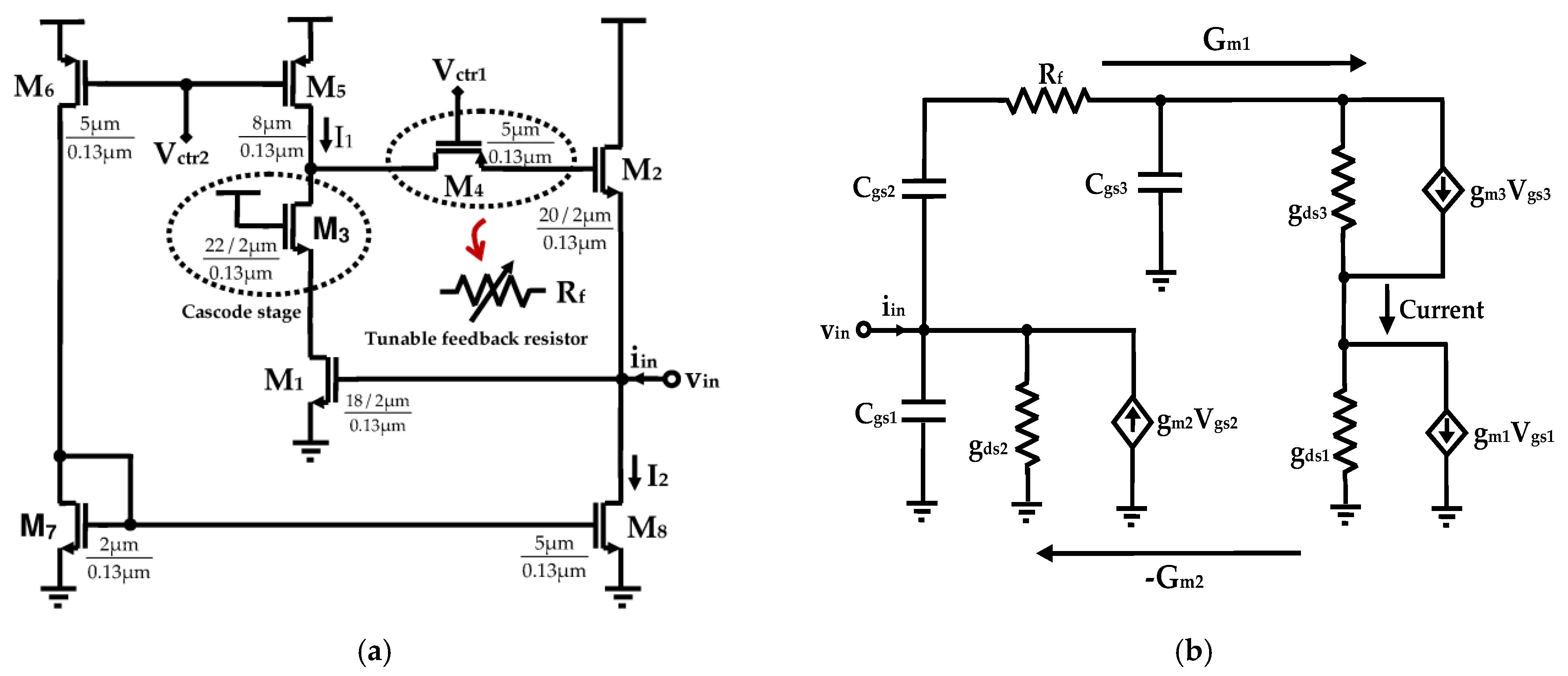
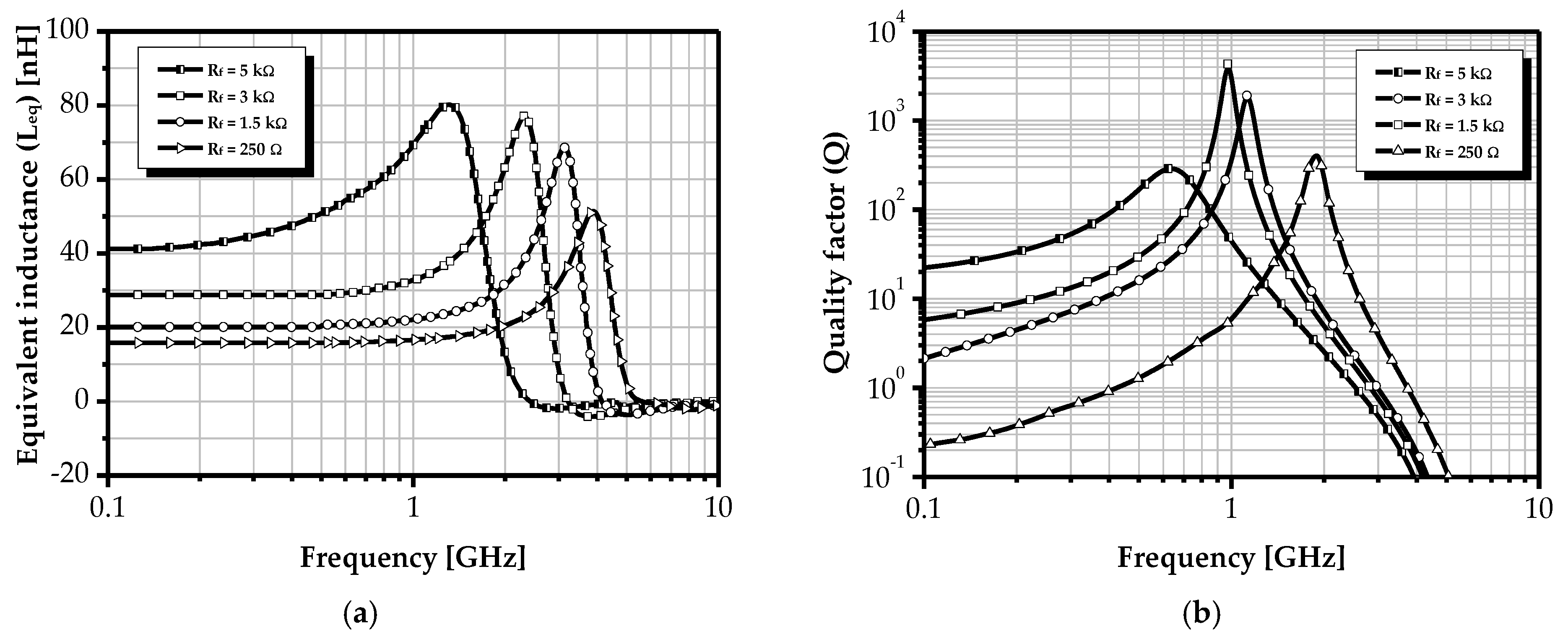
2.2. Proposed Grounded Tunable Active Inductor

The grounded active inductor topology [23,32] remains a widely adopted approach for emulating inductive behavior in integrated circuits, leveraging the well-established gyrator-C architecture. In this configuration, two active devices are arranged to generate an inductive input impedance, with the overall performance primarily determined by the choice of transconductor types. As shown in Figure 4, the fundamental transconductor configurations include the common-source (CS) structure exhibiting negative transconductance, and the common-drain (CD) and common-gate (CG) structures, which provide positive transconductance.
To address the limitations of conventional active inductor topologies, namely, low inductance values and a narrow frequency range for achieving high quality factors Q, this work employs an enhanced design strategy that integrates cascode and feedback-based techniques. Cascode and regulated cascode configurations are introduced to reduce the output conductance of the transistors, thereby decreasing the equivalent series resistance Rs and improving the quality factor [33]. To further enhance performance, a feedback resistor Rf is incorporated between the transconductance stages. This feedback path concurrently increases the equivalent inductance Leq and reduces Rs, thus enhancing the overall Q of the circuit [34]. As Rf also affects the self-resonant frequency and the frequency at which the maximum quality factor is achieved, i.e., f(Qmax), making Rf tunable provides independent control of L, Q, and f(Qmax), a key requirement for realizing a fully tunable active inductor (TAI).
The active inductor proposed in this work, along with its corresponding small-signal equivalent circuit, is depicted in Figure 5a,b. It consists of a single-port grounded structure, formed by two transconductors connected in a back-to-back configuration. Transistor M1 functions as a transconductor with negative transconductance in a common-source topology, while transistor M2 provides positive transconductance in a common-drain topology. All transistors operate in the saturation region to ensure proper biasing and linear operation.
A cascode transistor M3 is employed in the feedback path to enhance the quality factor Q by increasing the DC gain, resulting in a reduction in the series resistance Rs. This reduction leads to a lower zero frequency, thereby broadening the effective inductive frequency range. In addition, transistor M4, operating in the linear region, functions as a feedback resistor Rf. By decreasing Rs via the feedback resistance, the quality factor is further improved. The resistance can be tuned over a desired range by adjusting the gate voltage Vctr1.
The circuit shown in Figure 5a requires two current sources to bias transistors M1, M3, and M2. Transistors M5, M6, M7, and M8 serve as the source supply terminals, where M5 sources current I1, and M8 sinks current and supplies I2 to the active inductor.
The parallel capacitance Cp, parallel resistance Rp, series resistance Rs, and equivalent inductance Leq of the active inductor are derived as shown in Equations (9), (10), (11), and (12), respectively. For simplification, certain parasitic elements such as the impedance output of transistors and the gate–drain capacitance Cgd are neglected.
C p = C gs 1
R p = 1 + g ds 3 R f g ds 3 2 + g ds 3 R f
R s = g ds 1 g ds 3 g m 2 + ω 2 C gs 2 2 g m 3 C gs 2 C gs 3 g m 2 1 + g ds 3 R f g m 1 g m 3 g m 2 2 + ω 2 C gs 2 2 g m 1 g m 3
L eq = C gs 2 g m 2 g m 3 + ω 2 C gs 2 2 C gs 3 1 + g ds 3 R f g m 1 g m 3 g m 2 2 + ω 2 C gs 2 2 g m 1 g m 3
Assuming g m 2 2 > > ω 2 C gs 2 2 , the equivalent inductance Leq can be approximated by:
L eq = C gs 2 g m 2 g m 3 + ω 2 C gs 2 2 C gs 3 1 + g ds 3 R f g m 1 g m 3 g m 2 2
where gds1, gds2, and gds3 denote the output conductances; Cgs1, Cgs2, and Cgs3 represent the gate-source capacitances at nodes 1, 2, and 3, respectively; and gm1, gm2, and gm3 are the transconductances of transistors M1, M2, and M3, respectively.
From Equation (13), it is evident that the equivalent inductance exhibits an inverse relationship with the transconductance gm3, which is determined by the current flowing through M3. In this design, the cascode stage, implemented by transistor M3, is used to control the inductance. Lowering the gate voltage of M3 increases its drain current, which also impacts the drain current sourced by M5. Given that transconductance is defined as g m = I D / V G S = 2 μ n C o x W L I D , an increase in drain current results in a higher gm3, thereby leading to a reduction in Leq.
The quality factor of the active inductor is given by:
Q = C gs 2 g m 2 g m 3 ω + ω 3 C gs 2 2 C gs 3 ( R f g ds 3 + 1 ) g ds 1 g ds 3 g m 2 + ω 2 ( C gs 2 2 g m 3 C gs 2 C gs 3 g m 2 ( R f g ds 3 + 1 ) )
The zero frequency ωz and the self-resonant frequency ω0, which establish the operational frequency boundaries, are expressed as:
ω z = g ds 1 g ds 3 g m 2 + ω 2 C gs 2 2 g m 3 C gs 2 C gs 3 g m 2 1 + g ds 3 R f C gs 2 g m 2 g m 3 + ω 2 C gs 2 2 C gs 3 1 + g ds 3 R f
ω 0 = g m 1 g m 3 g m 2 2 + ω 2 C gs 2 2 g m 1 g m 3 C gs 1 C gs 2 g m 2 g m 3 + ω 2 C gs 2 2 C gs 1 C gs 3 1 + g ds 3 R f
Since the additional inductive reactance introduced by the feedback resistor Rf appears in the expressions for both the quality factor Q and the equivalent inductance Leq, its influence varies as a function of this resistance.
As indicated by Equation (14), and from the associated Equations (11) and (12), the inclusion of a cascode stage contributes to a reduction in the equivalent series resistance, as gm3 < 1, thereby improving the quality factor. Moreover, the incorporation of a feedback resistor Rf significantly enhances Q by simultaneously increasing Leq and reducing Rs. By tuning Rf, it is possible to adjust both the inductance and the quality factor. However, as shown by Equation (17) and illustrated in Figure 6, a substantial increase in Rf results in a pronounced reduction in fQ, the frequency at which the quality factor reaches its maximum. To mitigate this limitation, a secondary tuning mechanism is introduced via variation in the output conductance gds5, which is controlled using the voltage Vctr2. Consequently, simultaneous tuning of Vctr1 and Vctr2 enables the realization of the desired inductance and high-Q performance at the target operating frequency fQ.
f Q 1 2 π g m 3 + g ds 1 g ds 3 C gs 2 C gs 2 ( R f g ds 3 + 1 ) + C gs 3 ( 2 R f g ds 3 + 1 )
It is evident that both Leq and Q are strongly dependent on the value of Rf. Specifically, the inductance increases proportionally with Rf. Simulation results indicate that the inductance varies from 51 nH to 80 nH over a frequency range of 1.32 GHz to 3.88 GHz. From the analysis of the corresponding plots, it is observed that the variation in the quality factor with frequency exhibits a parabolic profile within the inductive operating region. The quality factor increases with Rf until it reaches a maximum value of 3942 at 0.987 GHz. Beyond this point, despite continued increases in Rf, the quality factor gradually decreases. This behavior can be explained by the increasing influence of resistive effects, particularly series parasitic resistance, which are minimal near the frequency where the quality factor is maximized but become more prominent outside that range. Additionally, increasing Rf causes a downward shift in the resonance frequency. These findings validate the effectiveness of the proposed method, maintaining a quality factor greater than 250 across the frequency range 0.62 GHz to 1.97 GHz.
The relationships between the principal circuit parameters considered in the parametric analysis and optimization process are summarized in Table 1 [35].

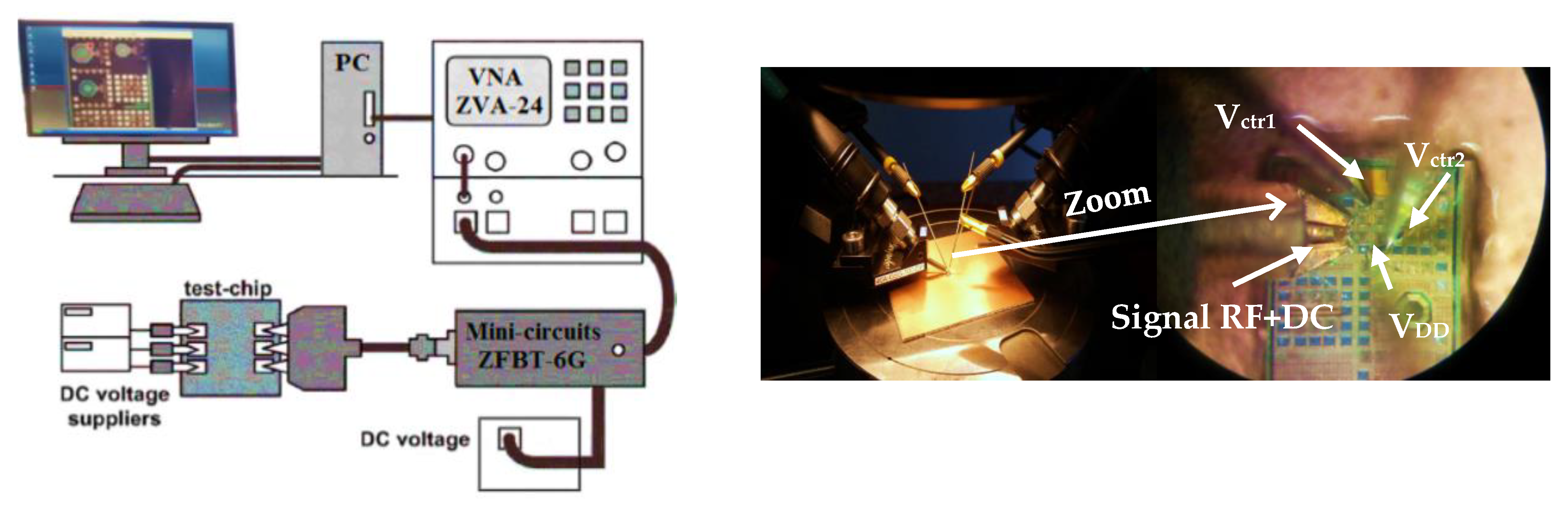
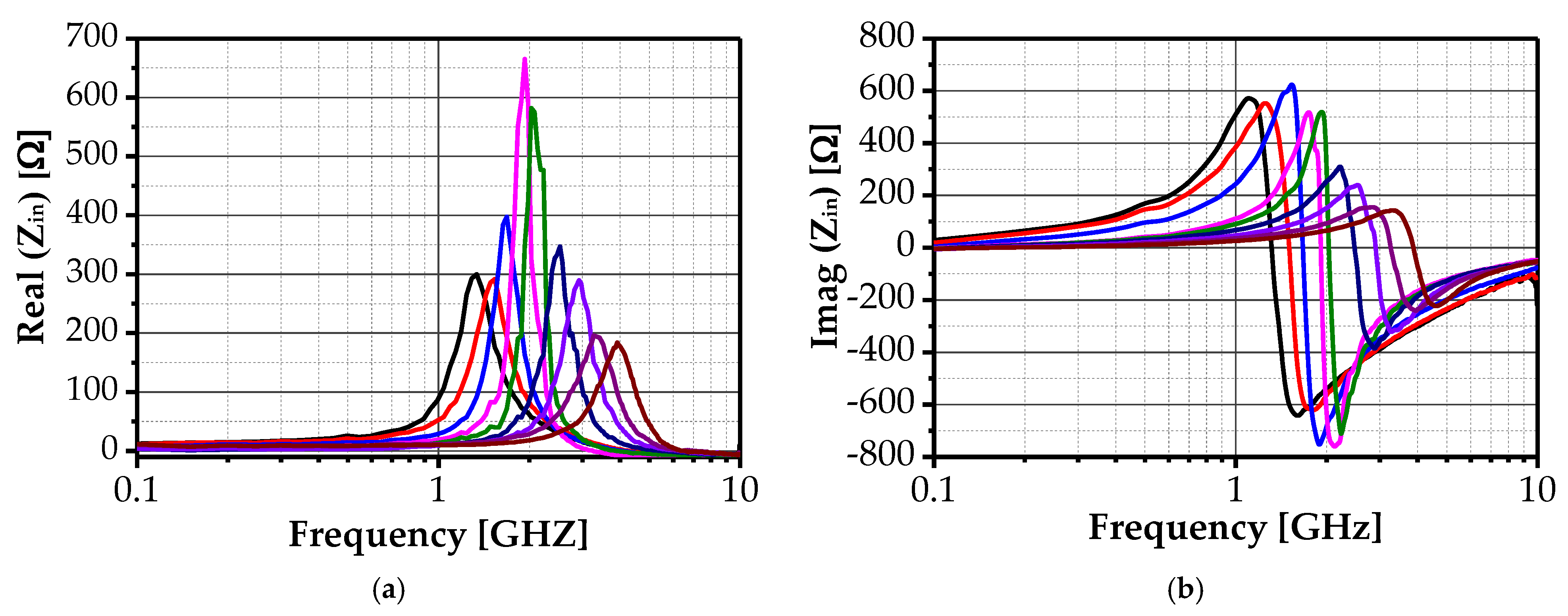
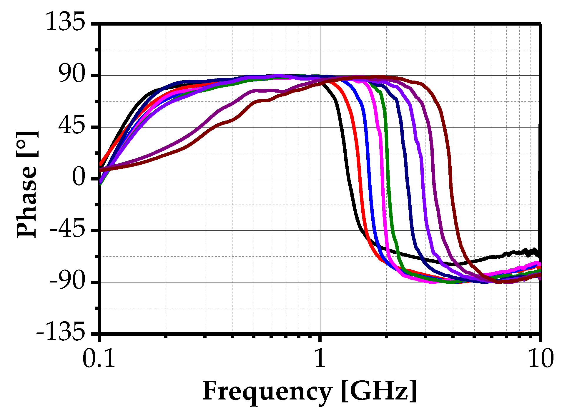
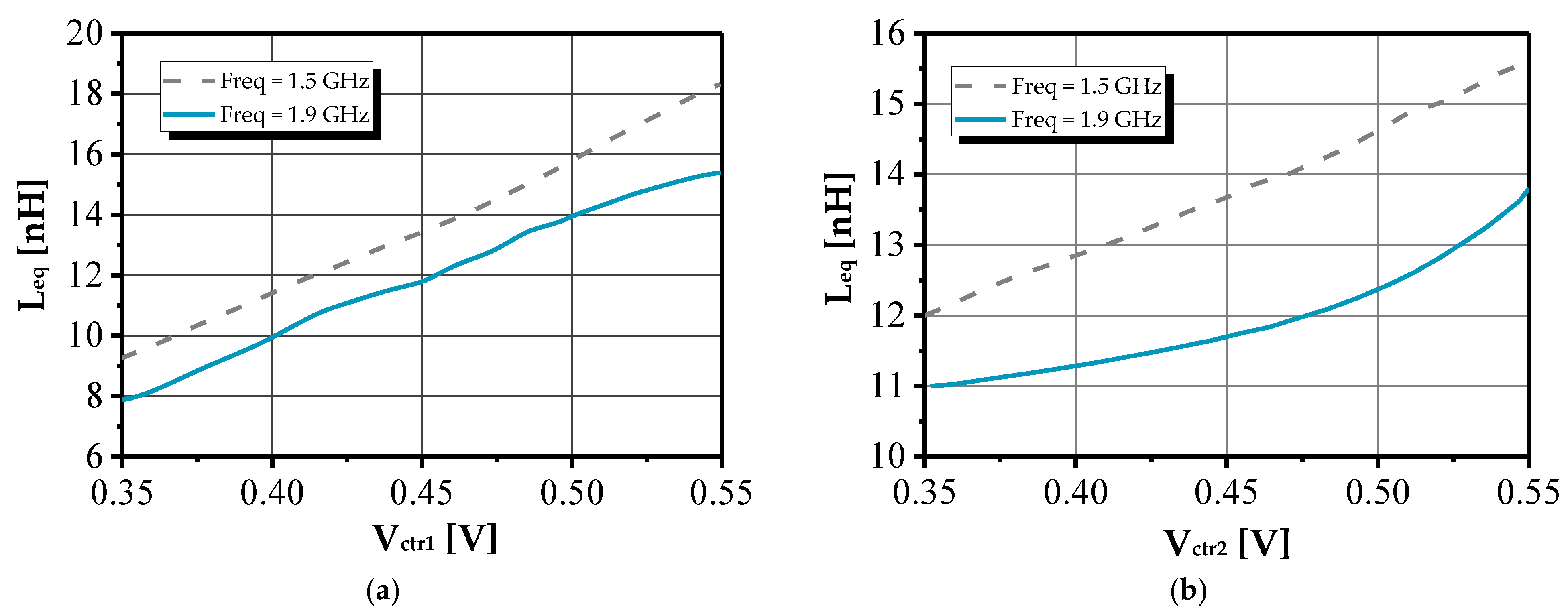
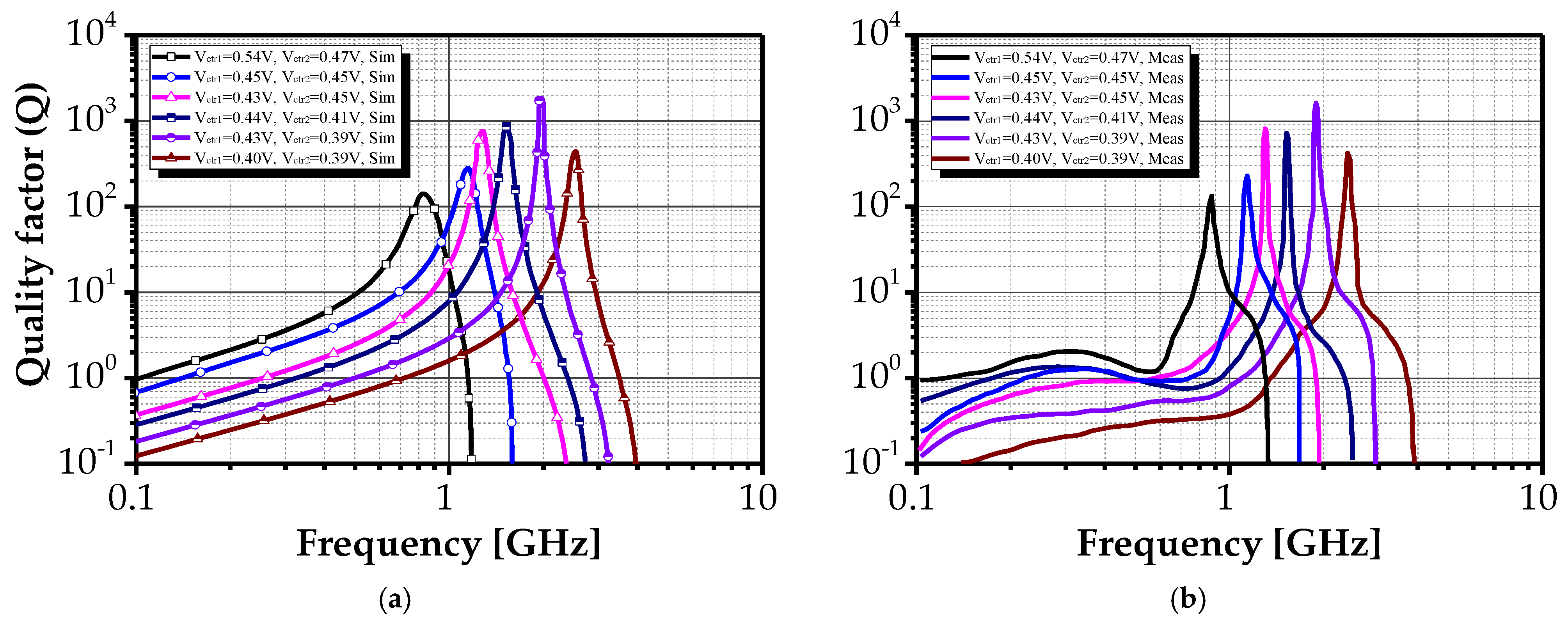
3. Experimental Results

The proposed grounded tunable active inductor was implemented using 0.13 μm STMicroelectronics CMOS technology as proof of concept. Fabrication and characterization were conducted under nominal process–voltage–temperature (PVT) conditions. All presented results correspond to this typical corner. Measurements were carried out on 25 fabricated chips, which exhibited a tightly clustered performance distribution, thereby confirming the design’s consistency and reliability under standard operating conditions. Figure 7 shows the die photographs of a fabricated chip, occupying an area of 400 μm × 345 μm including bond pads and of 25.3 μm × 12.2 μm without bond pads.
The top right corner of Figure 8 depicts the active inductor during testing, while the left side illustrates the test-bench environment. To ensure accurate measurement results, performance metrics were analyzed after de-embedding the loading effects introduced by the input RF pads. The 20 pF decoupling capacitors were implemented on-chip. On-wafer measurements were performed using a Rohde & Schwarz ZVA-24 vector network analyzer (VNA) with RF and DC probing. The measurements were conducted under a 1 V supply with an input signal amplitude of –20 dBm (27°) at 2 GHz. The measured power consumption of the grounded active inductor was 2.0 mW, primarily attributed to the gyrator-C core.
One-port S-parameter measurements obtained from the VNA demonstrate the variation in the magnitude and self-resonant frequency of Z11 as functions of the control voltages Vctr1 and Vctr2. As depicted in Figure 9a,b, sweeping Vctr1 from 0.3 V to 0.54 V and Vctr2 from 0.39 V to 0.47 V enables the self-resonant frequency tuning of the Z11 imaginary part from 1.08 GHz to 3.9 GHz and of the Z11 real part from 1.337 GHz to 3.96 GHz. This tunability is accompanied by variations in the magnitude of the impedance components, validating the inductor operational flexibility and the adopted reconfiguration methodology effectiveness.
Figure 10 presents the measured phase of the input impedance, delineating the operational frequency range of the inductor. The circuit begins exhibiting inductive characteristics at 87 MHz (ωz), with the phase angle reaching 45° at 150 MHz and peaking near 89°, maintaining inductive behavior up to 3.96 GHz (ω0), where the phase returns to 0°.
Based on the measured S-parameters, both the equivalent inductance and the quality factor Q were extracted, providing further validation of the inductor’s performance. Figure 11 illustrates the influence of control voltages Vctr1 and Vctr2 on the equivalent inductance, with VDD = 1 V. Measurements were conducted under two conditions: with Rf fixed and with the conductance gds5 held constant. The equivalent inductance Leq exhibits linear tuning behavior, as shown in Figure 11a,b, with the quality factor peaking at approximately 1.5 GHz and 1.9 GHz.
Figure 12 further demonstrates that inductance values can be adjusted over a wide frequency range (668 MHz to 3.96 GHz), with corresponding inductance variation from 84.4 nH to 6.7 nH. Figure 13 presents measured quality factor values for various control voltage settings, showing high Q values (up to 50) across frequency-independent bands. The maximum recorded quality factor of 1586 was achieved at 1.9 GHz under bias voltages Vctr1 = 0.43 V and Vctr2 = 0.41 V. The measurement trends in Figure 11 and Figure 12 align with those discussed in §2.2, confirming the design’s expected behavior.
Nevertheless, due to parasitic effects in the fabricated structure, the measured values of Leq and Q differ slightly from the simulation results. Such discrepancies are typical in practical implementations, where parasitic capacitances, resistances, and layout-related effects influence circuit behavior. The quality factor naturally varies with frequency due to the frequency-dependent characteristics of the transconductors. Slight shifts in equivalent inductance and self-resonant frequency were also observed, with some measured values exceeding simulation predictions.
A primary factor contributing to variations in the quality factor is the frequency-dependent behavior of the transconductors, wherein the transconductance gm decreases slightly at higher frequencies, thereby affecting the impedance transformation. Additional degradation arises from parasitic capacitances, specifically the gate-source (Cgs) and gate-drain (Cgd) capacitances, along with the finite output resistance of the transistors, all of which introduce losses that reduce the quality factor across most frequencies. Furthermore, deviations in fabrication processes, such as reduced oxide thickness or variations in interconnect geometry, can alter effective parasitic capacitances, exacerbating this anomaly. In practical RFIC implementations, such fluctuations in the quality factor can impair circuit performance, leading to diminished selectivity in bandpass filters, increased insertion loss in impedance matching networks, and degraded phase noise characteristics in oscillators.
Table 2 provides a comparative performance analysis between the proposed active inductor fabricated in this work and previously reported designs in the literature. The proposed design achieves an inductance tuning range of 6.7 nH to 84.4 nH, significantly broader than those reported in prior works, which typically remain below 25 nH. Although the design in Ref. [28] reports an inductance of 191 nH, this value lacks experimental verification and thus remains to be validated. Furthermore, the proposed design achieves a maximum quality factor Qmax of 1586, which substantially exceeds other reported values, such as the value of 28 in Ref. [36] and the value of 45 in Ref. [37]. The power consumption of the active inductors in Refs. [37,38] is reported to be 21 mW and 16 mW, respectively, exceeding the 2 mW consumption of the proposed design by more than ten and eight times, respectively. A further advantage of the proposed inductor is its compact layout area of 308 µm2, which is significantly smaller than those of existing designs (typically ranging from 3200 to 8200 µm2), enhancing its suitability for integration in compact RF systems.
Nevertheless, certain trade-offs are inherent. The wide tunability and high Q performance render the design more sensitive to variations in bias voltage, necessitating accurate bias stabilization to ensure consistent operation under process and temperature fluctuations. This requirement may increase overall system-level design complexity. Furthermore, the design may exhibit reduced linearity at higher signal amplitudes, which could constrain its applicability in circuits demanding high linearity, such as precision low-noise amplifiers.

4. Conclusions and Future Works

In this paper, a high-quality CMOS grounded active inductor has been presented. It was optimized in 130 nm CMOS technology. By incorporating a feedback resistor into a cascode grounded configuration, the proposed design achieves significant improvements in both inductance and quality factor. Experimental validation has demonstrated a maximum quality factor of 1586 and an inductance tuning range of 6.7 nH to 84.4 nH, with a low power consumption of only 2 mW.
The inductive bandwidth of the design is tunable across a frequency range of 87 MHz to 3.96 GHz, offering high versatility for diverse receiver applications. It is compatible with multiple mobile communication bands, including 4G and 5G NR (FR1) bands (n1, n3, n5, n7, n8, n20, n28, n38, n41, and n78), as well as the 2.4–2.5 GHz ISM band, enabling its integration into wireless system designs.
Our future work will be focused on further optimizing the design to extend its frequency tuning range and enhance its integration with advanced circuit architectures, aiming to improve overall performance and adaptability.

Author Contributions

Conceptualization, S.S. and A.B.H.; methodology, A.B.H.; software, A.B.H.; validation, S.S., A.B.H. and F.H.; formal analysis, A.B.H.; investigation, S.S.; resources, A.B.H.; data curation, S.S.; writing—original draft preparation, S.S. and A.B.H.; writing—review and editing, S.S. and F.H.; visualization, S.S. and A.B.H.; supervision, F.H. All authors have read and agreed to the published version of the manuscript.

Funding

This research received no external funding.

Institutional Review Board Statement

Not applicable.

Informed Consent Statement

Not applicable.

Data Availability Statement

Data are contained within the article.

Acknowledgments

The authors would like to think Fayrouz Haddad for their extraordinary support in this research project and for providing the essential resources that facilitated the preparation of this manuscript.

Conflicts of Interest

Author Aymen Ben Hammadi was employed by the company Dynamics RF/mmW Consulting and Design. The remaining authors declare that the research was conducted in the absence of any commercial or financial relationships that could be construed as a potential conflict of interest.

Abbreviations

The following abbreviations are used in this manuscript:
RFRadio frequency
CMOSComplementary metal-oxide semiconductor
AIActive inductor
GSGGround–signal–ground
SRFSelf-resonant frequency
NRNew Radio
FR1Frequency Range 1
5GFifth generation
FDDFrequency Division Duplex
TDDTime Division Duplex
LNALow-noise amplifier
VCOVoltage-controlled oscillator
NICNegative impedance converter
FinFETFin field-effect transistor
SOISilicon-on-insulator
GaNGallium nitride
KCLKirchhoff’s Current Law
CDCommon drain
CGCommon gate
CSCommon source
TAITunable active inductor
DCDirect current
VNAVector network analyzer
PVTProcess–voltage–temperature
4GFourth generation
ISMIndustrial, scientific, and medical

References

  1. Holma, H.; Toskala, A.; Nakamura, T. 5G Technology: 3GPP New Radio, 1st ed.; John Wiley & Sons: Hoboken, NJ, USA, 2020. [Google Scholar]
  2. Kim, Y.; Kim, Y.; Oh, J.; Ji, H.; Yeo, J.; Choi, S.; Ryu, H.; Noh, H.; Kim, T.; Sun, F.; et al. New radio (NR) and its evolution toward 5G-advanced. IEEE Wirel. Commun. 2019, 26, 2–7. [Google Scholar] [CrossRef]
  3. Lin, X.; Li, J.; Baldemair, R.; Cheng, J.F.T.; Parkvall, S.; Larsson, D.C.; Koorapaty, H.; Frenne, M.; Falahati, S.; Grovlen, A.; et al. 5G new radio: Unveiling the essentials of the next generation wireless access technology. IEEE Commun. Stand. Mag. 2019, 3, 30–37. [Google Scholar] [CrossRef]
  4. Ahmadi, S. 5G NR: Architecture, Technology, Implementation, and Operation of 3GPP New Radio Standards, 1st ed.; Academic Press: Cambridge, MA, USA, 2019. [Google Scholar]
  5. Chen, J.; Liou, J.J. On-chip spiral inductors for RF applications: An overview. J. Semicond. Technol. Sci. 2004, 4, 149–167. [Google Scholar]
  6. Yuce, E.; Minaei, S. Other Active Devices. In Passive and Active Circuits by Example, 1st ed.; Springer: Berlin/Heidelberg, Germany, 2024. [Google Scholar]
  7. Yuce, E.; Minaei, S. A modified CFOA and its applications to simulated inductors, capacitance multipliers, and analog filters. IEEE Trans. Circuits Syst. I Regul. Pap. 2008, 55, 266–275. [Google Scholar] [CrossRef]
  8. Dogan, M.; Yuce, E. CFOA based a new grounded inductor simulator and its applications. Microelectron. J. 2019, 90, 297–305. [Google Scholar] [CrossRef]
  9. Kacar, F.; Kuntman, H. CFOA-based lossless and lossy inductance simulators. Radioengineering 2011, 20, 627–631. [Google Scholar]
  10. Bang, J.; Ryu, I.H. Design of A 10MHz Bandpass Filter Using Grounding and Floating CDTA Active Inductors. J. Korea Acad.-Ind. Coop. Soc. 2014, 15, 6804–6809. [Google Scholar]
  11. Jaikla, W.; Biolek, D.; Siripongdee, S.; Bajer, J. High input impedance voltage-mode biquad filter using VD-DIBAs. Radioengineering 2014, 23, 914–921. [Google Scholar]
  12. Jaikla, W.; Bunrueangsak, S.; Khateb, F.; Kulej, T.; Suwanjan, P.; Supavarasuwat, P. Inductance simulators and their application to the 4th order elliptic lowpass ladder filter using CMOS VD-DIBAs. Electronics 2021, 10, 684. [Google Scholar] [CrossRef]
  13. Singh, Y.S.; Ranjan, A.; Adhikari, S.; Shimray, B.A. A lossless active inductor design using single ZC-VDCC: Grounded and floating mode. IETE J. Res. 2024, 70, 623–637. [Google Scholar] [CrossRef]
  14. Metin, B.; Herencsar, N.; Koton, J.; Horng, J.W. DCCII-based novel lossless grounded inductance simulators with no element matching constrains. Radioengineering 2014, 23, 532–539. [Google Scholar]
  15. Gür, F.; Anday, F. Simulation of a novel current-mode universal filter using FDCCIIs. Analog Integr. Circuits Signal Process. 2009, 60, 231–236. [Google Scholar] [CrossRef]
  16. Ferri, G.; Guerrini, N.; Silverii, E.; Tatone, A. Vibration damping using CCII-based inductance simulators. IEEE Trans. Instrum. Meas. 2008, 57, 907–914. [Google Scholar] [CrossRef]
  17. Senani, R.; Bhaskar, D.R.; Singh, A.K. Current Conveyors: Variants, Applications and Hardware Implementations, 1st ed.; Springer: Berlin/Heidelberg, Germany, 2014. [Google Scholar]
  18. Ibrahim, M.A.; Minaei, S.; Yuce, E.; Herencsar, N.; Koton, J. Lossy/Lossless Floating/Grounded Inductance Simulation Using One DDCC. Radioengineering 2012, 21, 3–10. [Google Scholar]
  19. Abaci, A.; Yuce, E. Single DDCC− based simulated floating inductors and their applications. IET Circuits Devices Syst. 2020, 14, 796–804. [Google Scholar] [CrossRef]
  20. Kumari, S.; Nand, D. Realization of nth Order Wave Active Low-Pass Filter Using Differential Difference Current Conveyor. J. Circuits Syst. Comput. 2024, 33, 2450180. [Google Scholar] [CrossRef]
  21. Tarunkumar, H.; Shantikumar Singh, Y.; Ranjan, A. An active inductor employing a new four terminal floating nullor transconductance amplifier (FTFNTA). Int. J. Electron. 2020, 107, 683–702. [Google Scholar] [CrossRef]
  22. Rani, M.; Kaur, P.A. Review of Active Inductors based on the Gyrator-C Principle. In Latest Trends in Engineering and Technology, 1st ed.; CRC Press: London, UK, 2024; pp. 205–213. [Google Scholar]
  23. Yuan, F. CMOS Active Inductors and Transformers: Principle, Implementation and Applications, 1st ed.; Springer: New York, NY, USA, 2008. [Google Scholar]
  24. Yücehan, T.; Yüce, E. A Lossless Simulated Floating Inductor Based on the Second-Generation Current Conveyors. Electrica 2025, 25, 1–13. [Google Scholar]
  25. Hsiao, C.C.; Kuo, C.W.; Ho, C.C.; Chan, Y.J. Improved quality-factor of 0.18-μm CMOS active inductor by a feedback resistance design. IEEE Microw. Wirel. Compon. Lett. 2002, 12, 467–469. [Google Scholar] [CrossRef]
  26. Yuce, E.; Alpaslan, H.; Minaei, S.; Ayten, U.E. A new simulated grounded inductor based on two NICs, two resistors and a grounded capacitor. Circuits Syst. Signal Process. 2021, 40, 5847–5863. [Google Scholar] [CrossRef]
  27. Behera, P.; Siddique, A.; Delwar, T.S.; Biswal, M.R.; Choi, Y.; Ryu, J.Y. A novel 65 nm active-inductor-based VCO with improved Q-factor for 24 GHz automotive radar applications. Sensors 2022, 22, 4701. [Google Scholar] [CrossRef] [PubMed]
  28. Gorjizad, Z.; Shojaee, A.; Abrishamifar, A. A compact and tunable active inductor-based bandpass filter with high quality factor for Wireless LAN applications. AEU—Int. J. Electron. Commun. 2024, 187, 155540. [Google Scholar] [CrossRef]
  29. Demirel, H.; Ahmed, A. New FinFet Transistor Implementation of Floating and Grounded Inductance Simulator Based on Active Elements. Gazi Mühendislik Bilimleri Dergisi 2024, 9, 647–653. [Google Scholar] [CrossRef]
  30. Yang, R.; Li, J.; Qian, H.; Han, Z. SOI active and passive integrated devices for RFIC applications. In Proceedings of the 7th International Conference on Solid-State and Integrated Circuits Technology, Beijing, China, 18–21 October 2004; Volume 1, pp. 186–189. [Google Scholar]
  31. Herbert, T.B.; Hyland, J.S.; Abdullah, S.; Wight, J.; Amaya, R.E. An active bandpass filter for LTE/WLAN applications using robust active inductors in gallium nitride. IEEE Trans. Circuits Syst. II Express Briefs 2021, 68, 2252–2256. [Google Scholar] [CrossRef]
  32. Ismail, M.; Wassenaar, R.; Morrison, W. A high-speed continuous-time bandpass VHF filter in MOS technology. In Proceedings of the 1991 IEEE International Symposium on Circuits and Systems (ISCAS), Singapore, 11–14 June 1991; pp. 1761–1764. [Google Scholar]
  33. Ler, C.L.; A’ain, A.K.B.; Kordesch, A.V. CMOS active inductor linearity improvement using feed-forward current source technique. IEEE Trans. Microw. Theory Tech. 2009, 57, 1915–1924. [Google Scholar] [CrossRef]
  34. Mukhopadhyay, R.; Park, Y.; Sen, P.; Srirattana, N.; Lee, J.; Lee, C.H.; Nuttinck, S.; Joseph, A.; Cressler, J.; Laskar, J. Reconfigurable RFICs in Si-based technologies for a compact intelligent RF front-end. IEEE Trans. Microw. Theory Tech. 2005, 53, 81–93. [Google Scholar] [CrossRef]
  35. Zaiden, D.M.; Grandfield, J.E.; Weller, T.M.; Mumcu, G. Compact and wideband MMIC phase shifters using tunable active inductor-loaded all-pass networks. IEEE Trans. Microw. Theory Tech. 2017, 66, 1047–1057. [Google Scholar] [CrossRef]
  36. Hwang, K.S.; Cho, C.S.; Lee, J.W.; Kim, J. High quality-factor and inductance of symmetric differential-pair structure active inductor using a feedback resistance design. In Proceedings of the IEEE MTT-S International Microwave Symposium Digest, Atlanta, GA, USA, 15–20 June 2008; pp. 1059–1062. [Google Scholar]
  37. Ghadiri, A.; Moez, K. Wideband active inductor and negative capacitance for broadband RF and microwave applications. IEEE Trans. Compon. Packag. Manuf. Technol. 2014, 4, 1808–1814. [Google Scholar] [CrossRef]
  38. Bhattacharya, R.; Basu, A.; Koul, S.K. A highly linear CMOS active inductor and its application in filters and power dividers. IEEE Microw. Wirel. Compon. Lett. 2015, 25, 715–717. [Google Scholar] [CrossRef]
  39. Pakasiri, C.; Hsu, K.C.; Wang, S. A Compact 0.73~3.1 GHz CMOS VCO Based on Active-Inductor and Active-Resistor Topology. J. Low Power Electron. Appl. 2024, 14, 18. [Google Scholar] [CrossRef]
  40. Saad, S.; Mhiri, M.; Hammadi, A.B.; Besbes, K. A new low-power, high-Q, wide tunable CMOS active inductor for RF applications. IETE J. Res. 2016, 62, 265–273. [Google Scholar] [CrossRef]
  41. Koo, J.; An, B.; Jeong, Y. Wideband CMOS high-Q 2-port active inductor using parallel LC resonance Circuit. In Proceedings of the Asia-Pacific Microwave Conference (APMC), New Delhi, India, 5–9 December 2016; pp. 1–4. [Google Scholar]
Figure 1. (a) Lossy single-ended gyrator-C network-based AIs, and (b) the corresponding equivalent RLC model.
Sensors 25 03070 g001
Figure 2. Bode plot of input impedance Zin for a lossy single-ended gyrator-C active inductor.
Sensors 25 03070 g002
Figure 3. Influence of (a) Rp and (b) Rs on the quality factor of AIs, with Leq = 2.4 nH, Cp = 140 fF, Rs = 5 Ω, and Rp = 5 kΩ.
Sensors 25 03070 g003
Figure 4. Fundamental transconductor configurations: (a) common source, (b) common drain, and (c) common gate.
Sensors 25 03070 g004
Figure 5. (a) Proposed grounded gyrator-C-based active inductor topology and (b) the corresponding small signal equivalent circuit.
Sensors 25 03070 g005
Figure 6. Effect of feedback resistor Rf on (a) equivalent inductance and (b) the quality factor.
Sensors 25 03070 g006
Figure 7. Die micrograph of the fabricated active inductor.
Sensors 25 03070 g007
Figure 8. Experimental test-bench setup of the proposed active inductor.
Sensors 25 03070 g008
Figure 9. Measured input impedance of the proposed AI: (a) real part and (b) imaginary part.
Sensors 25 03070 g009
Figure 10. Measured phase response of the input impedance for the proposed AI.
Sensors 25 03070 g010
Figure 11. Variation in equivalent inductance and quality factor as a function of (a) Vctr1 with constant gds5 and (b) Vctr2 with fixed Rf.
Sensors 25 03070 g011
Figure 12. Input inductance values for the proposed AI’s input impedance under different control voltages Vctr1 and Vctr2: (a) simulated and (b) measured.
Sensors 25 03070 g012
Figure 13. Quality factor for the proposed AI’s input impedance under various control voltages Vctr1 and Vctr2: (a) simulated and (b) measured.
Sensors 25 03070 g013
Table 1. Optimization summary of tunable active inductor performance based on transconductance and feedback resistance variation.
gmωzω0RsLeqQ
+↓↓↓↓↑↑
↑↑↑↑↓↓
Rfωzω0RsLeqQ
+↓↓↑↓
↑↑↓↑
Table 2. Performance comparison summary of state-of-the-art active inductor implementations.
Ref.TopologyVerificationLeq (nH)QmaxSRF (GHz)PDC (mW)Area (µm²)CMOS
Process (nm)
VDD
(V)
[25]Gyrator-CMeas.5.7702.5888 × 90 +1802.0
[28]Gyrator-CSim.191.72864.81--651.2
[36]Gyrator-CMeas.27281.540.1 × 0.1 mm2 *1801.8
[37]Gyrator-CMeas.0.65–145>821390 × 290 +1301.5
[38]Gyrator-CMeas.0.8–3.5703.5168800 +1803.3
[39]Gyrator-CMeas.2.5–5740>6--1801.6
[40]Gyrator-CSim.3.55–268955.50.522 × 27.5 +901.0
[41]Gyrator-CMeas.22450103.60.2 × 0.3 +651.2
This workGyrator-CMeas.6.7–84.415863.96212.2 × 25.3 +1301.0
+ Without bond pads. * With bond pads.
Disclaimer/Publisher’s Note: The statements, opinions and data contained in all publications are solely those of the individual author(s) and contributor(s) and not of MDPI and/or the editor(s). MDPI and/or the editor(s) disclaim responsibility for any injury to people or property resulting from any ideas, methods, instructions or products referred to in the content.

