
Optically Controlled Gain Modulation for Microwave Metasurface Antennas
 ,
,
Abstract
1. Introduction
2. Photoconductive Principle
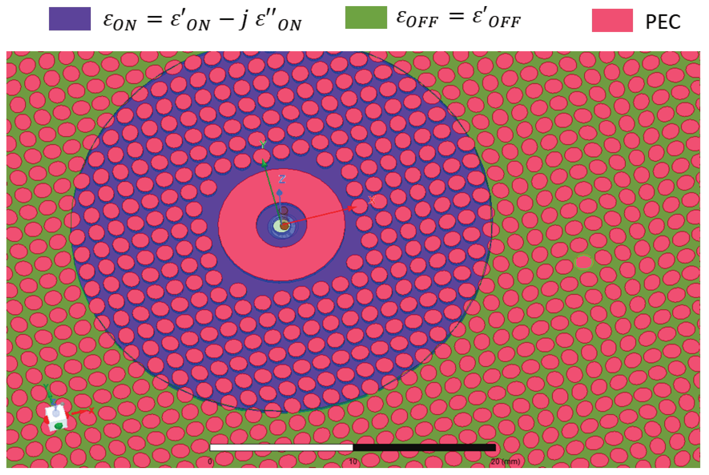
3. Ka-Band Metasurface Antenna on Silicon Substrate
3.1. Fabrication of the Metasurface on Silicon
3.2. Antenna Layout
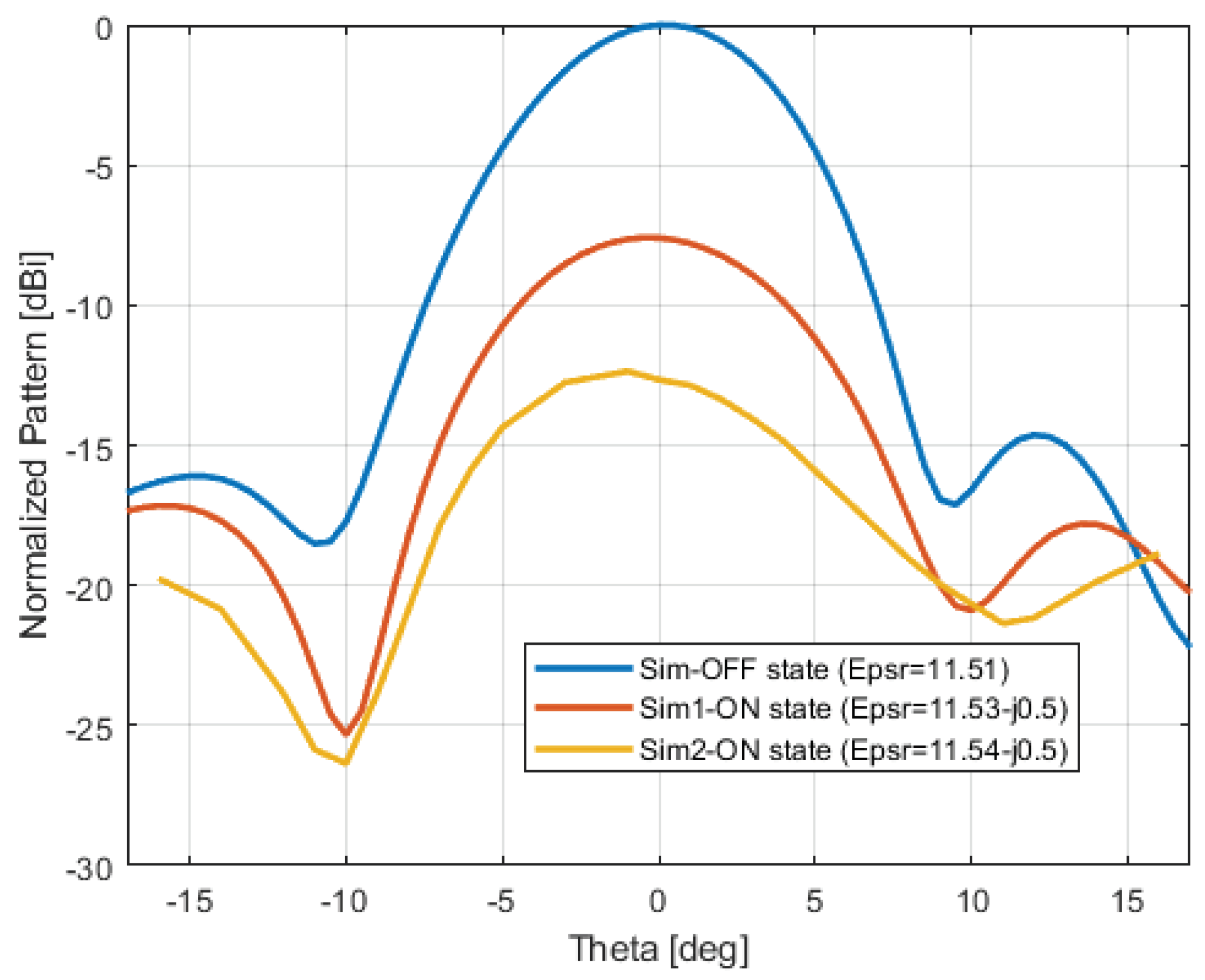
4. Numerical Model
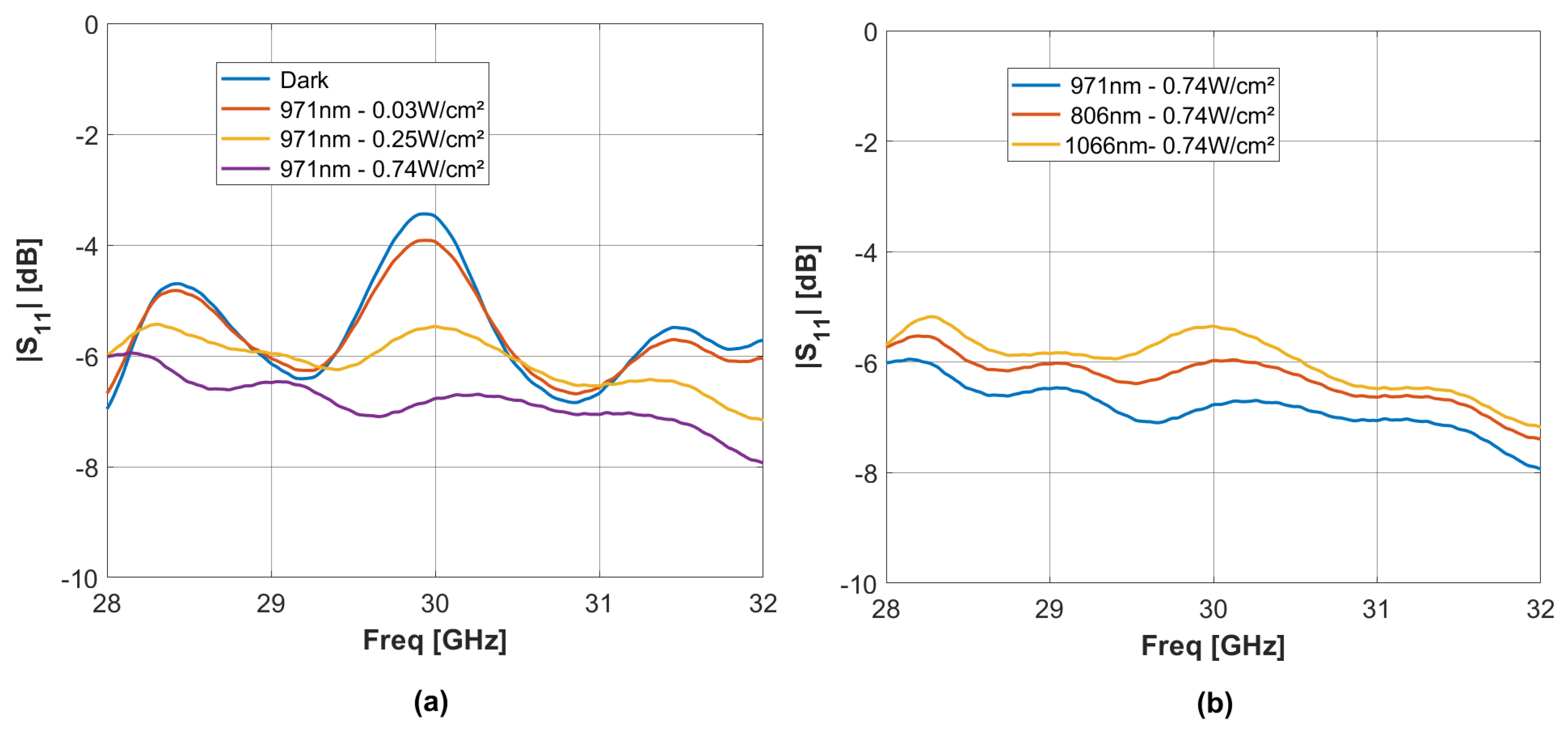
5. Optical Control and Antenna Gain Modulation
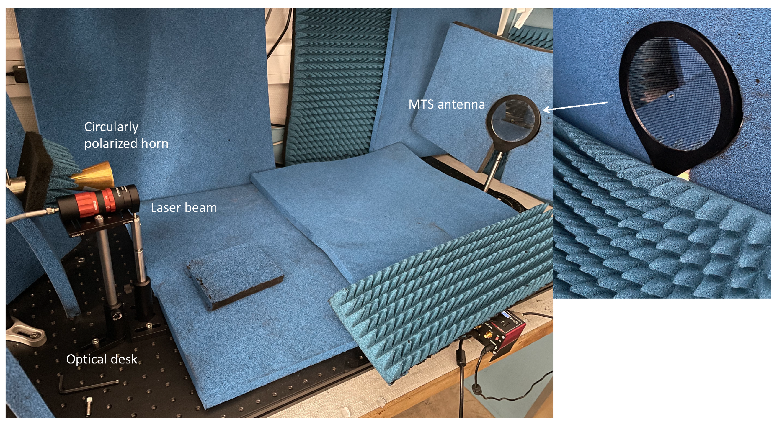
5.1. Experimental Setup and Measurements
5.2. Interpretation in Terms of Antenna Efficiency Contributions
6. Antenna Input Impedance
7. Conclusions and Discussion
Author Contributions
Funding
Institutional Review Board Statement
Informed Consent Statement
Data Availability Statement
Conflicts of Interest
References
- Yu, N.; Genevet, P.; Kats, M.A.; Aieta, F.; Tetienne, J.P.; Capasso, F.; Gaburro, Z. Light Propagation with Phase Discontinuities: Generalized Laws of Reflection and Refraction. Science 2011, 334, 333–337. [Google Scholar] [CrossRef]
- Pfeiffer, C.; Grbic, A. Metamaterial Huygens’ Surfaces: Tailoring Wave Fronts with Reflectionless Sheets. Phys. Rev. Lett. 2013, 110, 197401. [Google Scholar] [CrossRef]
- Asadchy, V.S.; Albooyeh, M.; Tcvetkova, S.N.; Díaz-Rubio, A.; Ra’di, Y.; Tretyakov, S.A. Perfect control of reflection and refraction using spatially dispersive metasurfaces. Phys. Rev. B 2016, 94, 075142. [Google Scholar] [CrossRef]
- Mohammadi Estakhri, N.; Alù, A. Wave-front Transformation with Gradient Metasurfaces. Phys. Rev. X 2016, 6, 041008. [Google Scholar] [CrossRef]
- Wong, J.P.S.; Epstein, A.; Eleftheriades, G.V. Reflectionless Wide-Angle Refracting Metasurfaces. IEEE Antennas Wirel. Propag. Lett. 2016, 15, 1293–1296. [Google Scholar] [CrossRef]
- Yepes, C.; Faenzi, M.; Maci, S.; Martini, E. Perfect non-specular reflection with polarization control by using a locally passive metasurface sheet on a grounded dielectric slab. Appl. Phys. Lett. 2021, 118, 231601. [Google Scholar] [CrossRef]
- Zhu, H.L.; Cheung, S.W.; Chung, K.L.; Yuk, T.I. Linear-to-Circular Polarization Conversion Using Metasurface. IEEE Trans. Antennas Propag. 2013, 61, 4615–4623. [Google Scholar] [CrossRef]
- Nama, L.; Nilotpal; Bhattacharyya, S.; Jain, P.K. A Metasurface-Based, Ultrathin, Dual-Band, Linear-to-Circular, Reflective Polarization Converter: Easing uplinking and downlinking for wireless communication. IEEE Antennas Propag. Mag. 2021, 63, 100–110. [Google Scholar] [CrossRef]
- Epstein, A.; Eleftheriades, G.V. Synthesis of Passive Lossless Metasurfaces Using Auxiliary Fields for Reflectionless Beam Splitting and Perfect Reflection. Phys. Rev. Lett. 2016, 117, 256103. [Google Scholar] [CrossRef]
- Zhang, X.; Deng, R.; Yang, F.; Jiang, C.; Xu, S.; Li, M. Metasurface-Based Ultrathin Beam Splitter with Variable Split Angle and Power Distribution. ACS Photonics 2018, 5, 2997–3002. [Google Scholar] [CrossRef]
- Sun, S.; He, Q.; Xiao, S.; Xu, Q.; Li, X.; Zhou, L. Gradient-index meta-surfaces as a bridge linking propagating waves and surface waves. Nat. Mater. 2012, 11, 426–431. [Google Scholar] [CrossRef]
- Qu, C.; Xiao, S.; Sun, S.; He, Q.; Zhou, L. A theoretical study on the conversion efficiencies of gradient meta-surfaces. Europhys. Lett. 2013, 101, 54002. [Google Scholar] [CrossRef]
- Tcvetkova, S.N.; Kwon, D.H.; Díaz-Rubio, A.; Tretyakov, S.A. Near-perfect conversion of a propagating plane wave into a surface wave using metasurfaces. Phys. Rev. B 2018, 97, 115447. [Google Scholar] [CrossRef]
- Tcvetkova, S.N.; Maci, S.; Tretyakov, S.A. Exact Solution for Conversion of Surface Waves to Space Waves by Periodical Impenetrable Metasurfaces. IEEE Trans. Antennas Propag. 2019, 67, 3200–3207. [Google Scholar] [CrossRef]
- Tcvetkova, S.N.; Martini, E.; Tretyakov, S.A.; Maci, S. Perfect Conversion of a TM Surface Wave Into a TM Leaky Wave by an Isotropic Periodic Metasurface Printed on a Grounded Dielectric Slab. IEEE Trans. Antennas Propag. 2020, 68, 6145–6153. [Google Scholar] [CrossRef]
- Minatti, G.; Faenzi, M.; Martini, E.; Caminita, F.; De Vita, P.; González-Ovejero, D.; Sabbadini, M.; Maci, S. Modulated Metasurface Antennas for Space: Synthesis, Analysis and Realizations. IEEE Trans. Antennas Propag. 2015, 63, 1288–1300. [Google Scholar] [CrossRef]
- Minatti, G.; Caminita, F.; Martini, E.; Maci, S. Flat Optics for Leaky-Waves on Modulated Metasurfaces: Adiabatic Floquet-Wave Analysis. IEEE Trans. Antennas Propag. 2016, 64, 3896–3906. [Google Scholar] [CrossRef]
- Minatti, G.; Caminita, F.; Martini, E.; Sabbadini, M.; Maci, S. Synthesis of Modulated-Metasurface Antennas with Amplitude, Phase, and Polarization Control. IEEE Trans. Antennas Propag. 2016, 64, 3907–3919. [Google Scholar] [CrossRef]
- Bodehou, M.; Khalifeh, K.A.; Jha, S.N.; Craeye, C. Direct Numerical Inversion Methods for the Design of Surface Wave-Based Metasurface Antennas: Fundamentals, Realizations, and Perspectives. IEEE Antennas Propag. Mag. 2022, 64, 24–36. [Google Scholar] [CrossRef]
- Budhu, J.; Szymanski, L.; Grbic, A. Design of Planar and Conformal, Passive, Lossless Metasurfaces That Beamform. IEEE J. Microwaves 2022, 2, 401–418. [Google Scholar] [CrossRef]
- Patel, A.M.; Grbic, A. Modeling and analysis of printed-circuit tensor impedance surfaces. IEEE Trans. Antennas Propag. 2013, 61, 211–220. [Google Scholar] [CrossRef]
- Gonzalez-Ovejero, D.; Martini, E.; Loiseaux, B.; Tripon-Canseliet, C.; Mencagli, M.; Chazelas, J.; Maci, S. Basic properties of checkerboard metasurfaces. IEEE Antennas Wirel. Propag. Lett. 2015, 14, 406–409. [Google Scholar] [CrossRef]
- Mencagli, M.; Martini, E.; Maci, S. Surface Wave Dispersion for Anisotropic Metasurfaces Constituted by Elliptical Patches. IEEE Trans. Antennas Propag. 2015, 63, 2992–3003. [Google Scholar] [CrossRef]
- Faenzi, M.; Gonzalez-Ovejero, D.; Maci, S.; Faenzi, M.; González-Ovejero, D.; Maci, S. Modulated Metasurface Antennas with Enhanced Broadband Response. EuCAP 2021, 2021, 10. [Google Scholar] [CrossRef]
- Faenzi, M.; Graziuso, N.; Martini, E.; Maci, S. Design Methods for Dual Polarized Metasurface Antennas: Three Simple Approaches. IEEE Antennas Propag. Mag. 2022, 64, 37–50. [Google Scholar] [CrossRef]
- Fong, B.H.; Colburn, J.S.; Ottusch, J.J.; Visher, J.L.; Sievenpiper, D.F. Scalar and tensor holographic artificial impedance surfaces. IEEE Trans. Antennas Propag. 2010, 58, 3212–3221. [Google Scholar] [CrossRef]
- Amendola, G.; Cavallo, D.; Chaloun, T.; Defrance, N.; Goussetis, G.; Margalef-Rovira, M.; Martini, E.; Quevedo-Teruel, O.; Valenta, V.; Fonseca, N.J.; et al. Low-Earth Orbit User Segment in the Ku and Ka-Band: An Overview of Antennas and RF Front-End Technologies. IEEE Microw. Mag. 2023, 24, 32–48. [Google Scholar] [CrossRef]
- Gupta, U.; Tan, A.; Liu, J.; Lohmeyer, W. Modern flat panel technology for Ku/Ka-band user terminal in LEO satellite communications systems. Microw. J. 2021, 64, 70. [Google Scholar]
- Herrán, L.F.; Algaba Brazalez, A.; Rajo-Iglesias, E. Ka-band planar slotted waveguide array based on groove gap waveguide technology with a glide-symmetric holey metasurface. Sci. Rep. 2021, 11, 8697. [Google Scholar] [CrossRef]
- Sun, J.; Li, T.; Dou, W. An Open-Ended Rectangular Waveguide Antenna with Metasurface at Ka-band. In Proceedings of the European Conference on Antennas and Propagation (EuCAP), Dusseldorf, Germany, 22–26 March 2021. [Google Scholar] [CrossRef]
- Li, T.; Chen, Z.N. Wideband Sidelobe-Level Reduced Ka-Band Metasurface Antenna Array Fed by Substrate-Integrated Gap Waveguide Using Characteristic Mode Analysis. IEEE Trans. Antennas Propag. 2020, 68, 1356–1365. [Google Scholar] [CrossRef]
- Zhang, Y.; Liu, H.; Meng, C.; Lin, Y.; Zhang, Y.; Forsberg, E.; He, S. A Broadband High-Gain Circularly Polarized Wide Beam Scanning Leaky-Wave Antenna. IEEE Access 2020, 8, 171091–171099. [Google Scholar] [CrossRef]
- Lim, W.H.; Moon, S.M.; Lee, H.L. Ka-band flat panel circularly polarized antenna array for LEO satellite communication systems. Alex. Eng. J. 2023, 78, 584–591. [Google Scholar] [CrossRef]
- Grabtchak, S.; Cocivera, M. Microwave response due to light-induced changes in the complex dielectric constant of semiconductors. Phys. Rev. B Condens. Matter Mater. Phys. 1998, 58, 4701–4707. [Google Scholar] [CrossRef]
- Ding, L.; Shih, I.; Pavlasek, T.J.; Champness, C.H. Measurements of the Photo-Induced Complex Permittivity of Si, Ge, and Te at 9 GHz. IEEE Trans. Microw. Theory Tech. 1984, 32, 151–157. [Google Scholar] [CrossRef]
- Tripon-Canseliet, C.; Faci, S.; Decoster, D.; Pagies, A.; Yoon, S.F.; Pey, K.L.; Chazelas, J. Nano photoconductive switches for microwave applications. Proc. Quantum Sens. Nanophotonic Devices X 2013, 8631, 216–221. [Google Scholar]
- Aileen M Vaucher, C.D.S.; Lee, C.H. Theory of Optically Controlled Millimeter-Wave Phase Shifters. IEEE Trans. Microw. Theory Tech. 1983, 31, 209–216. [Google Scholar] [CrossRef]
- Boone, D.E.; Jackson, C.H.; Swecker, A.T.; Hergenrather, J.S.; Wenger, K.S.; Kokhan, O.; Terzić, B.; Melnikov, I.; Ivanov, I.N.; Stevens, E.C.; et al. Probing the Wave Nature of Light-Matter Interaction. World J. Condens. Matter Phys. 2018, 8, 62–89. [Google Scholar] [CrossRef][Green Version]
- Forouzmand, A.; Salary, M.M.; Shirmanesh, G.K.; Sokhoyan, R.; Atwater, H.A.; Mosallaei, H. Tunable all-dielectric metasurface for phase modulation of the reflected and transmitted light via permittivity tuning of indium tin oxide. Nanophotonics 2019, 8, 415–427. [Google Scholar] [CrossRef]
- Krupka, J. Microwave measurements of electromagnetic properties of materials. Materials 2021, 14, 5097. [Google Scholar] [CrossRef] [PubMed]
- Kumar, R.J.; Borrego, J.M.; Gutmann, R.J.; Jenny, J.R.; Malta, D.P.; Hobgood, H.M.; Carter, C.H. Microwave photoconductivity decay characterization of high-purity 4H-SiC substrates. J. Appl. Phys. 2007, 102, 013704. [Google Scholar] [CrossRef]
- Makarov, S.V.; Zalogina, A.S.; Tajik, M.; Zuev, D.A.; Rybin, M.V.; Kuchmizhak, A.A.; Juodkazis, S.; Kivshar, Y. Light-Induced Tuning and Reconfiguration of Nanophotonic Structures. Laser Photonics Rev. 2017, 11, 1700108. [Google Scholar] [CrossRef]
- Sauerer, B.; Platte, W. Optically CW-induced losses in semiconductor coplanar waveguides. IEEE Trans. Microw. Theory Tech. 1989, 37, 139–149. [Google Scholar] [CrossRef]
- Krupka, J.; Kamiński, P.; Kozłowski, R.; Surma, B.; Dierlamm, A.; Kwestarz, M. Dielectric properties of semi-insulating silicon at microwave frequencies. Appl. Phys. Lett. 2015, 107, 082105. [Google Scholar] [CrossRef]
- Gamlath, C.D.; Benton, D.; Cryan, M.J. Microwave characterisation of optically illuminated silicon. In Proceedings of the 14th International Conference on Transparent Optical Networks (ICTON), Coventry, UK, 2–5 July 2012. [Google Scholar] [CrossRef]
- Yang, X.; Liu, X.; Yu, S.; Gan, L.; Zhou, J.; Zeng, Y. Permittivity of undoped silicon in the millimeter wave range. Electronics 2019, 8, 886. [Google Scholar] [CrossRef]
- Grabtchak, S.; Cocivera, M. Behavior of photoconductivity transients due to multiple trapping by a gaussian distribution of localized states. Phys. Rev. B Condens. Matter Mater. Phys. 1999, 60, 10997–11004. [Google Scholar] [CrossRef]
- Tripon-Canseliet, C.; Chazelas, J. Millimeter-Wave Permittivity Variations of an HR Silicon Substrate from the Photoconductive Effect. Micromachines 2022, 13, 1782. [Google Scholar] [CrossRef] [PubMed]
- Gabriele Minatti, E.M.; Maci, S. Efficiency of Metasurface Antennas. IEEE Trans. Antennas Propag. 2015, 63, 1532–1541. [Google Scholar] [CrossRef]


| Ref | Frequency (GHz) | Bandwidth (%) | Gain (dB) | Technology |
|---|---|---|---|---|
| [29] | 28.6 | - | 24.8 | PSWA |
| [30] | 29.1–32.5 | 11.3 | 9 | OERWA |
| [31] | 34 | 35.5 | 17.4 | SIWG |
| [32] | 26.5–40 | 40 | 12.5 | CSIW |
| [33] | 28 | 13.92 | 14.4 | PSP |
| this work | 30 | 20 | 20 | MTS |
| Power Density (W/cm²) | Main Lobe Gain Reduction (dB) |
|---|---|
| 0.03 | 2 |
| 0.25 | 4.6 |
| 0.74 | 6.8 |
| Wavelength (nm) | Main Lobe Gain Reduction (dB) |
|---|---|
| 808 | 6.7 |
| 971 | 6.8 |
| 1066 | 6.9 |
Disclaimer/Publisher’s Note: The statements, opinions and data contained in all publications are solely those of the individual author(s) and contributor(s) and not of MDPI and/or the editor(s). MDPI and/or the editor(s) disclaim responsibility for any injury to people or property resulting from any ideas, methods, instructions or products referred to in the content. |
© 2024 by the authors. Licensee MDPI, Basel, Switzerland. This article is an open access article distributed under the terms and conditions of the Creative Commons Attribution (CC BY) license (https://creativecommons.org/licenses/by/4.0/).
Share and Cite
Tripon-Canseliet, C.; Della Giovampaola, C.; Pavy, N.; Chazelas, J.; Maci, S. Optically Controlled Gain Modulation for Microwave Metasurface Antennas. Sensors 2024, 24, 1911. https://doi.org/10.3390/s24061911
Tripon-Canseliet C, Della Giovampaola C, Pavy N, Chazelas J, Maci S. Optically Controlled Gain Modulation for Microwave Metasurface Antennas. Sensors. 2024; 24(6):1911. https://doi.org/10.3390/s24061911
Chicago/Turabian StyleTripon-Canseliet, Charlotte, Cristian Della Giovampaola, Nicolas Pavy, Jean Chazelas, and Stefano Maci. 2024. "Optically Controlled Gain Modulation for Microwave Metasurface Antennas" Sensors 24, no. 6: 1911. https://doi.org/10.3390/s24061911
APA StyleTripon-Canseliet, C., Della Giovampaola, C., Pavy, N., Chazelas, J., & Maci, S. (2024). Optically Controlled Gain Modulation for Microwave Metasurface Antennas. Sensors, 24(6), 1911. https://doi.org/10.3390/s24061911