
The Design, Modeling and Experimental Investigation of a Micro-G Microoptoelectromechanical Accelerometer with an Optical Tunneling Measuring Transducer
 , ,
, ,
Abstract
1. Introduction
2. Designing Micromechanical Sensing Element of Accelerometer
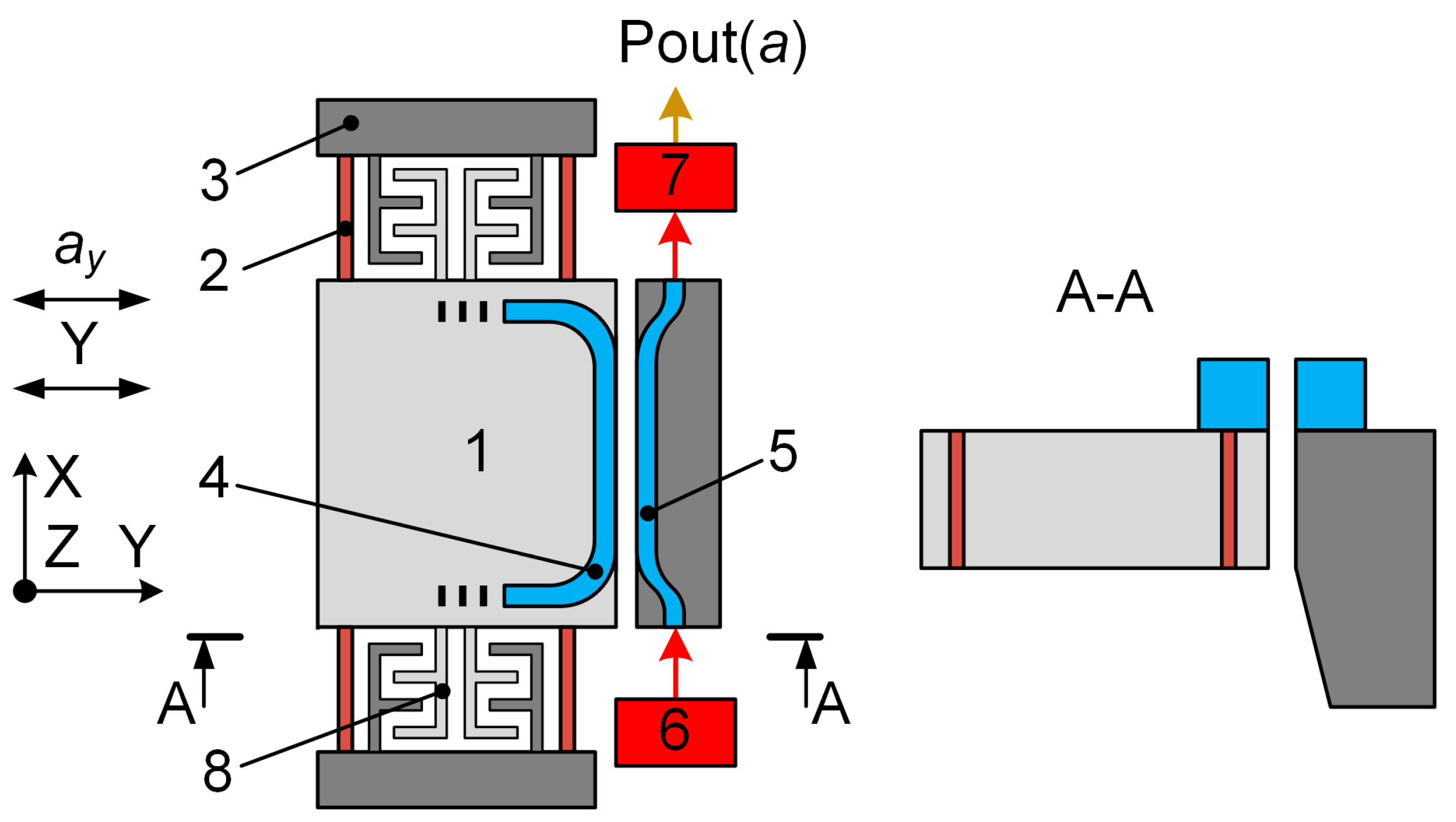
2.1. Functional Scheme
2.2. Mechanical Characteristics of the MSE
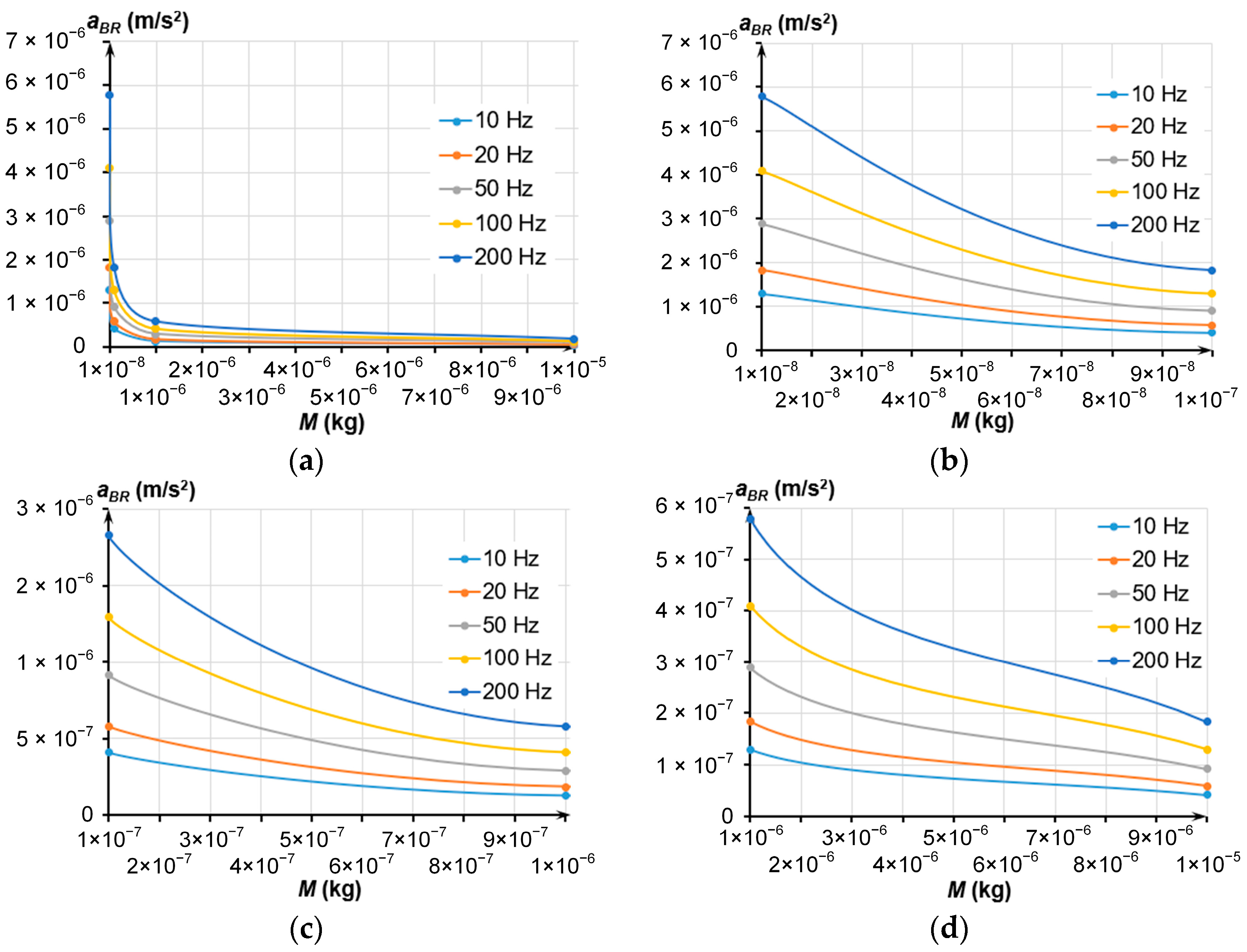
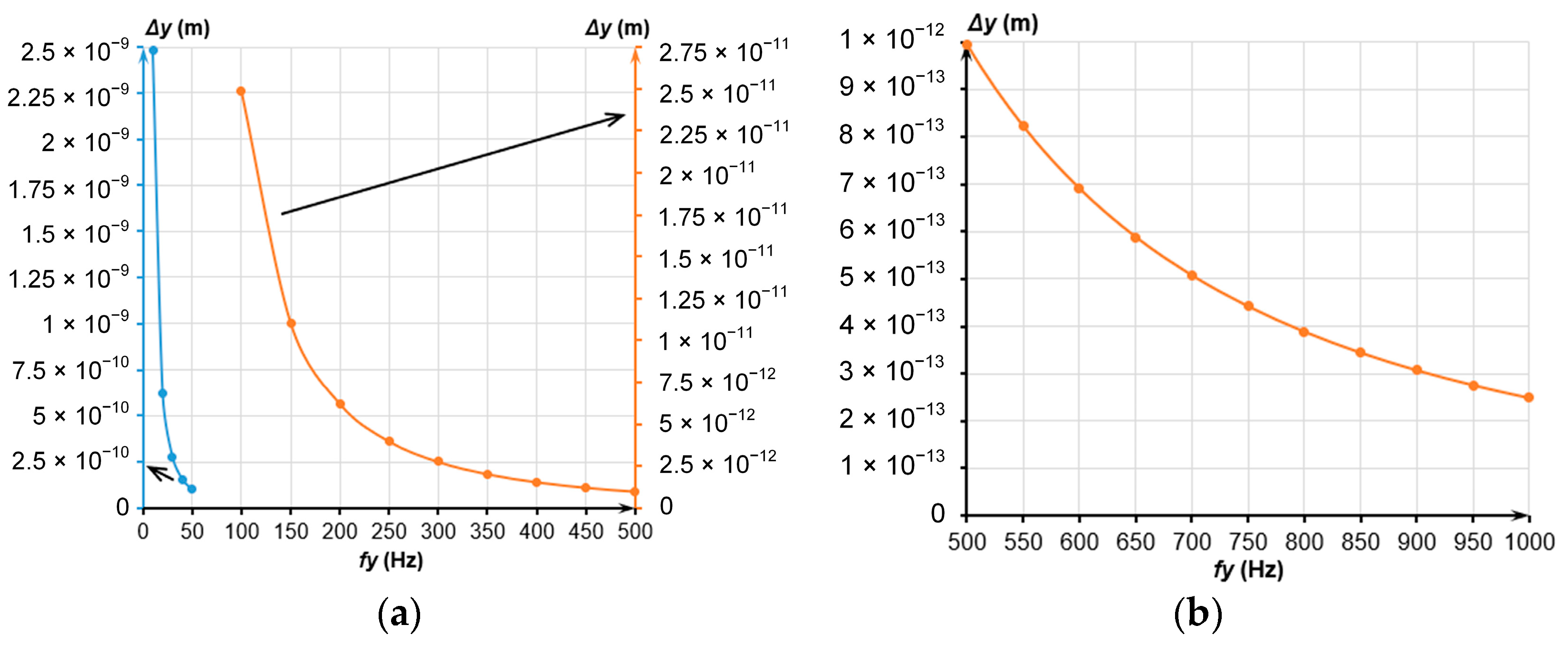
2.2.1. Dimensions, Mass, and Eigenfrequencies of the MSE
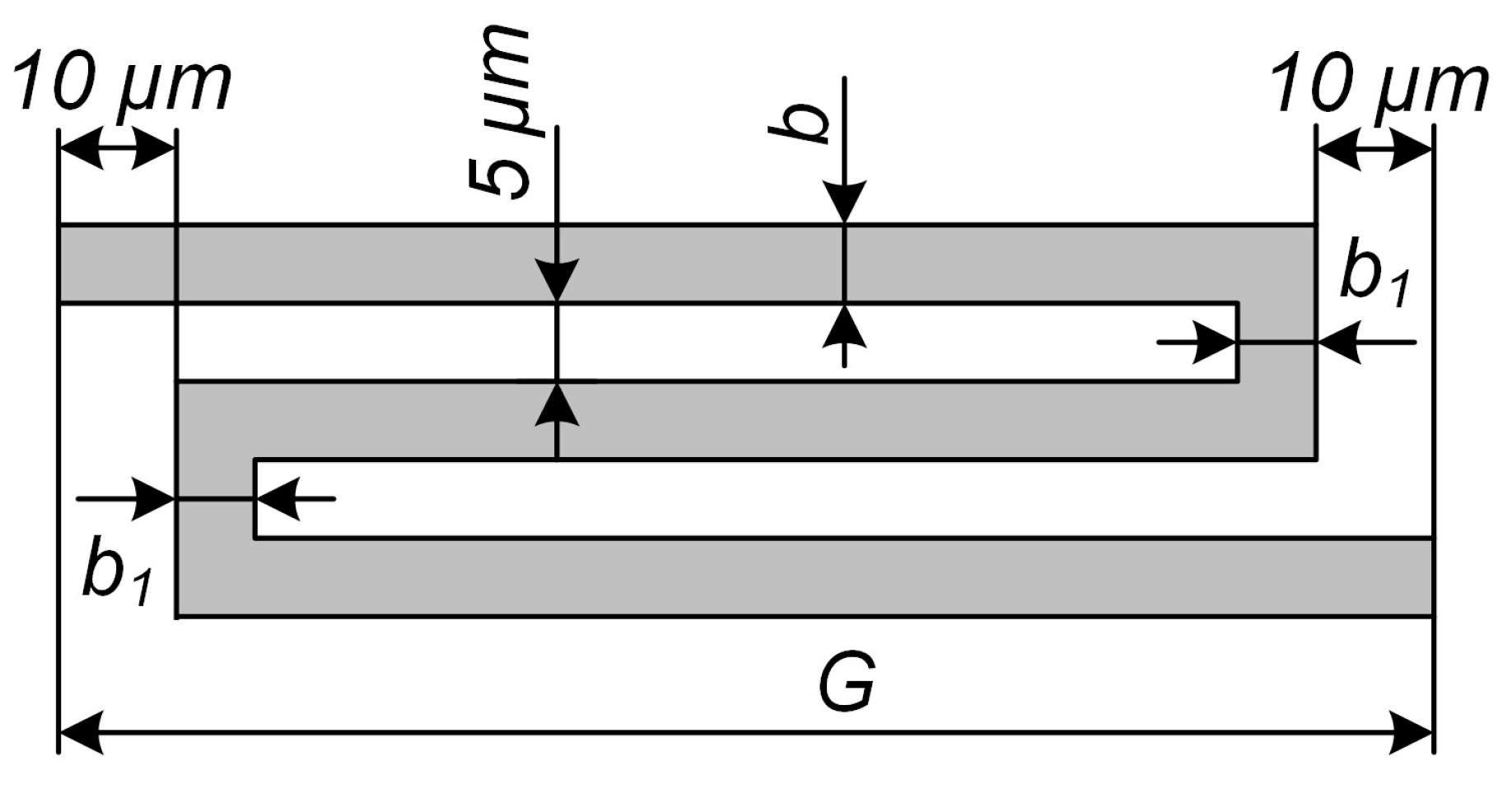
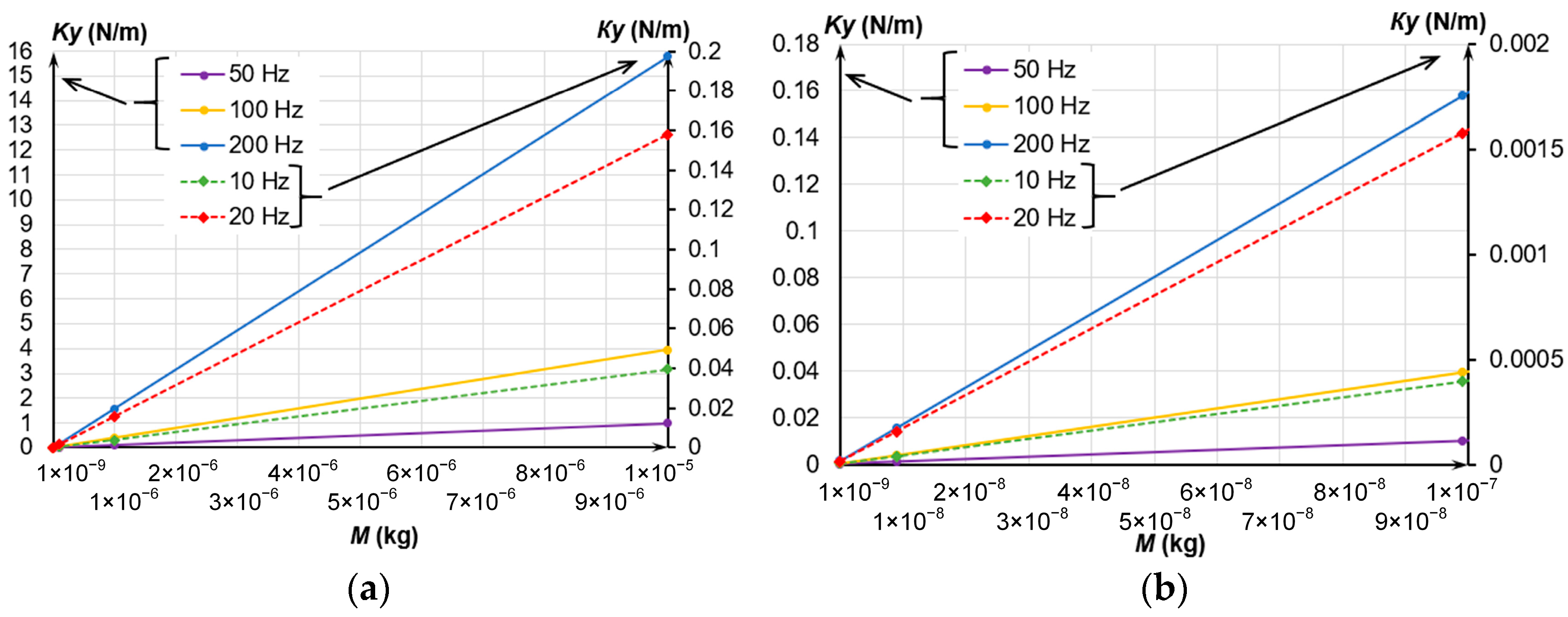
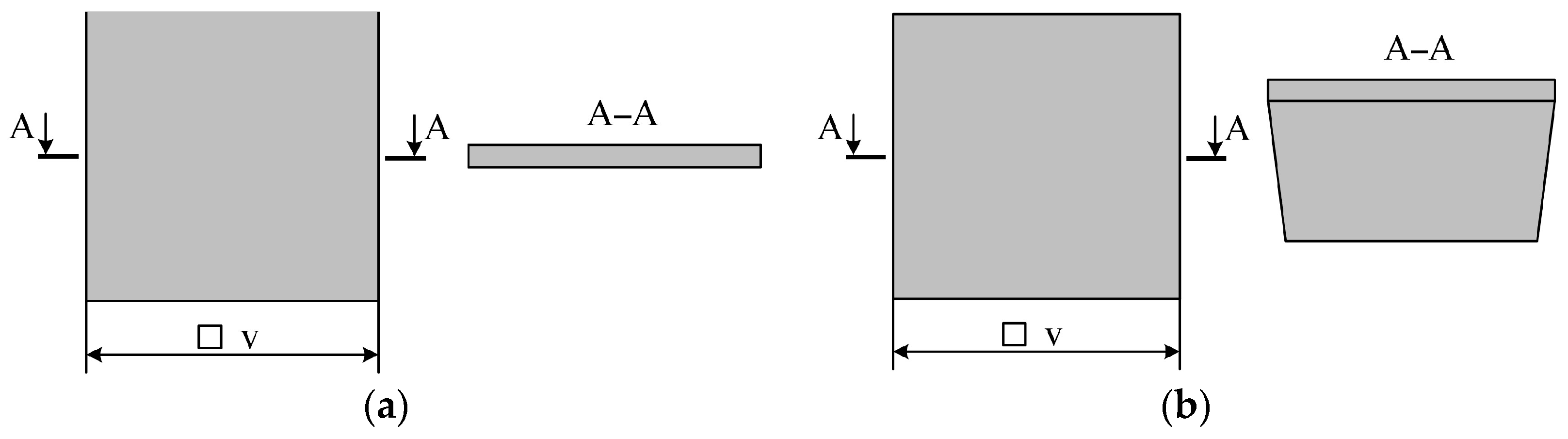
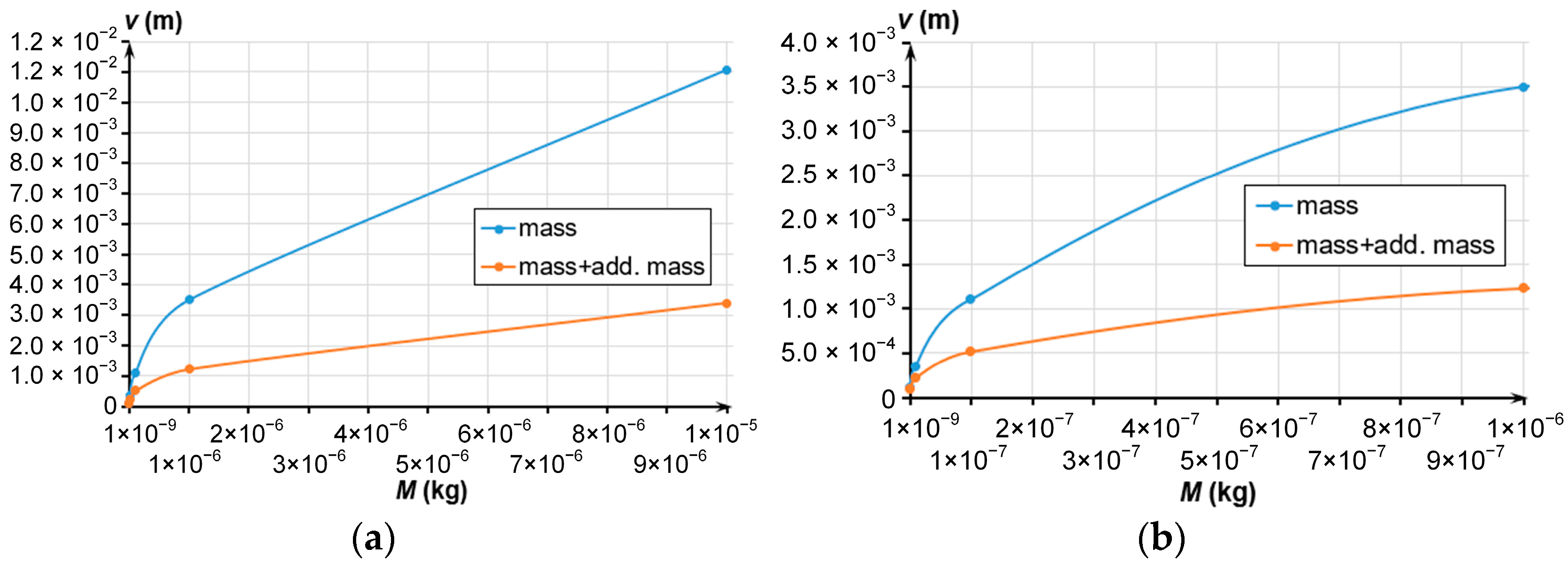
2.2.2. Spring Suspensions of the MSE
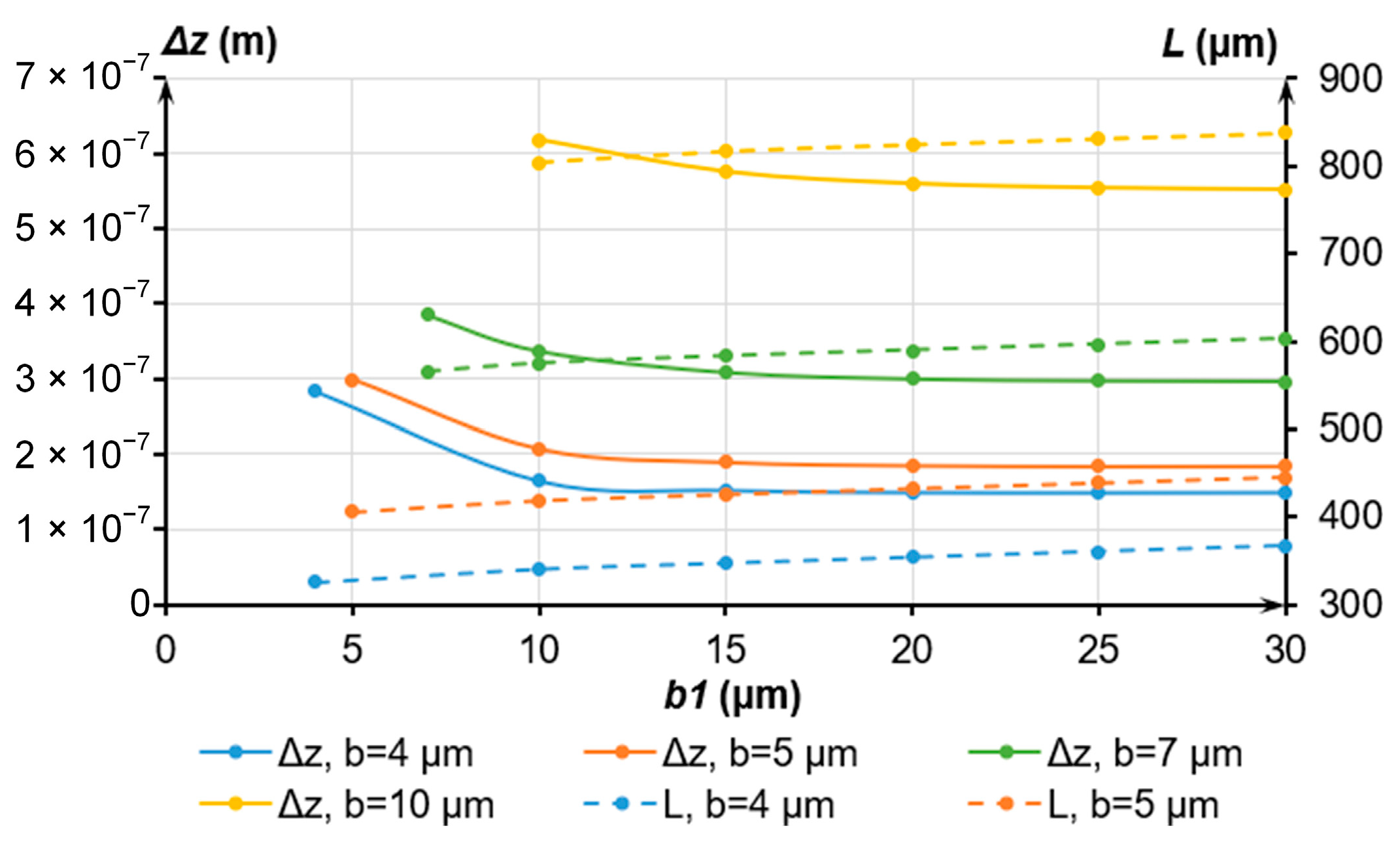
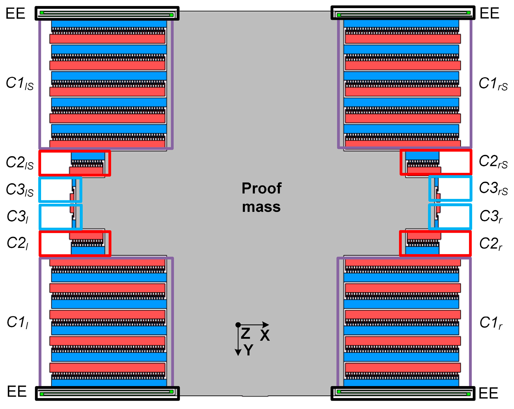
2.2.3. Optical Transducer Positioning System
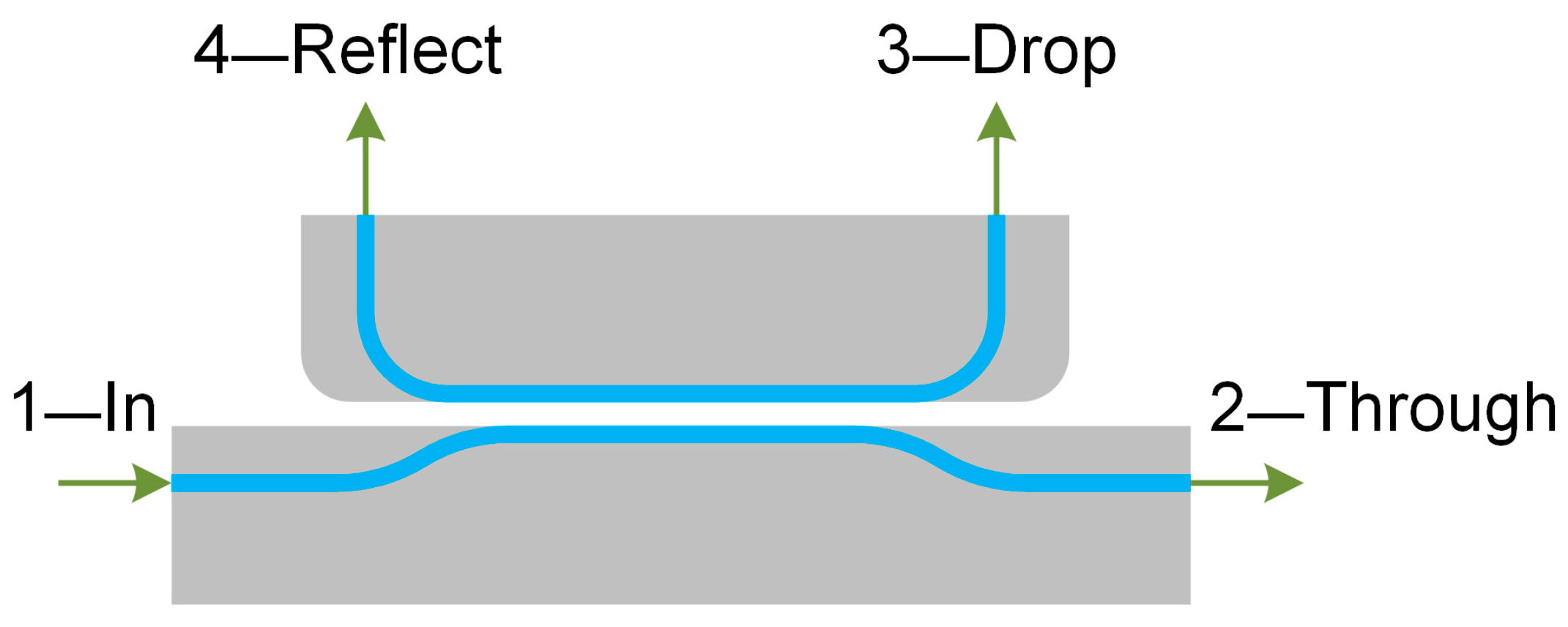
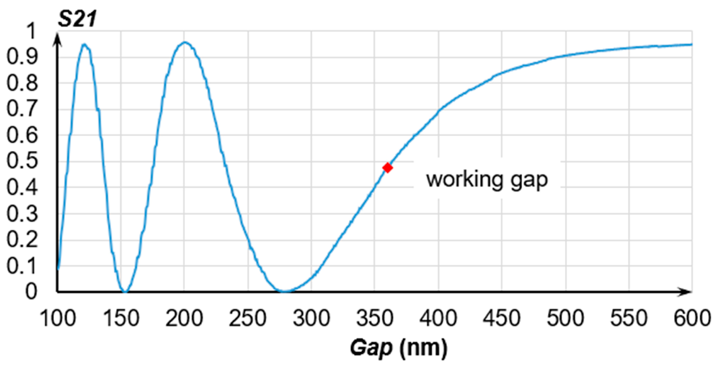
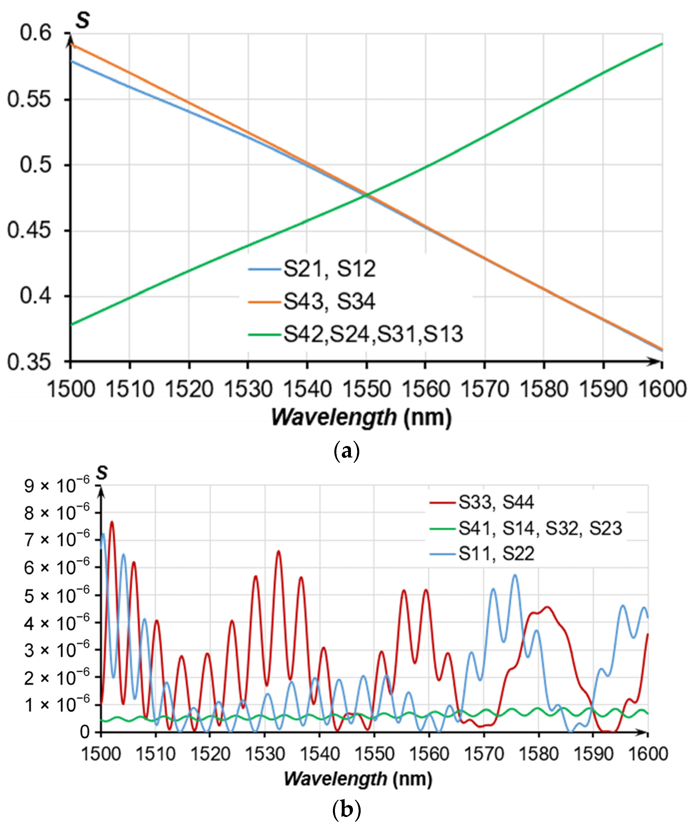
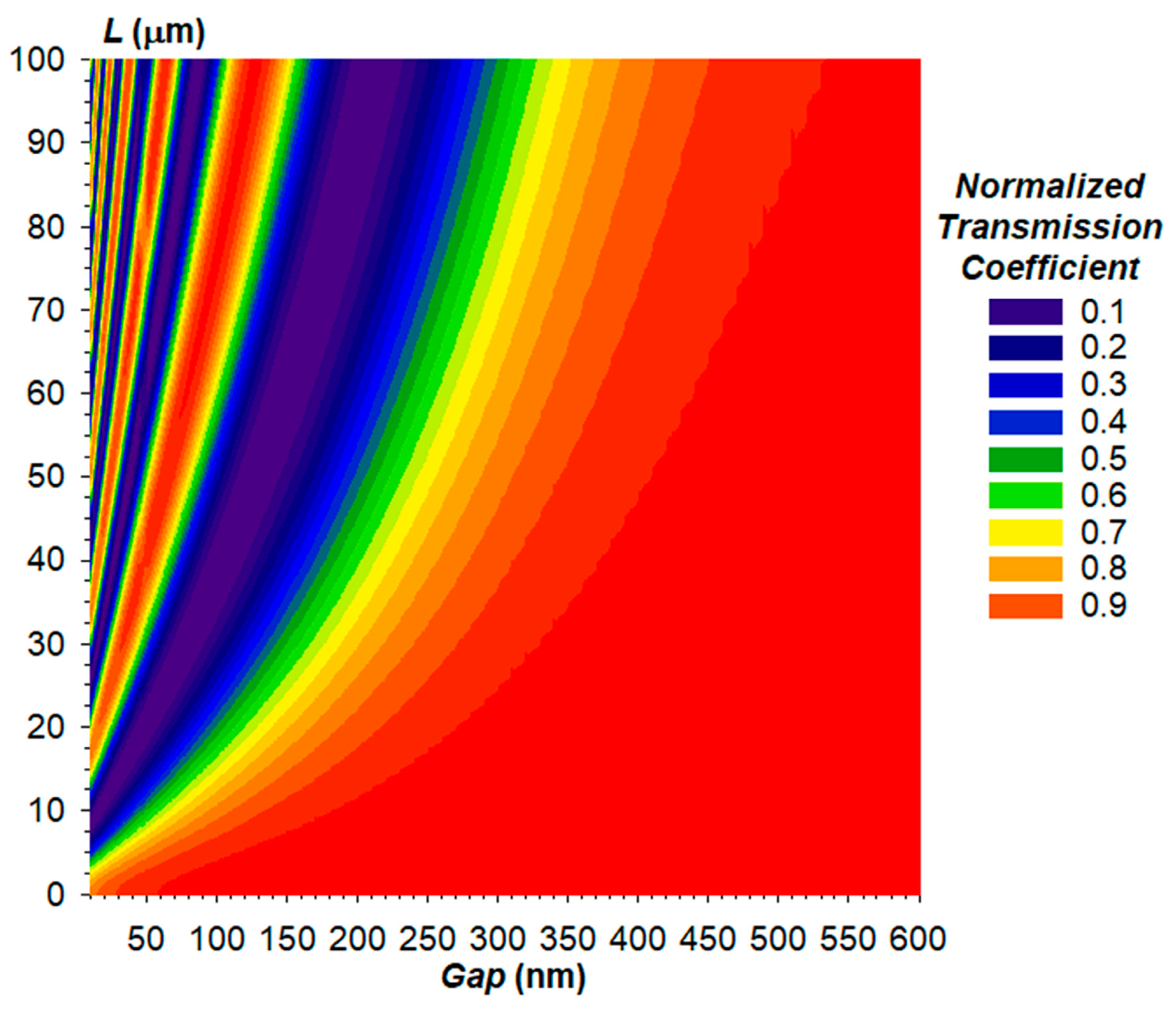
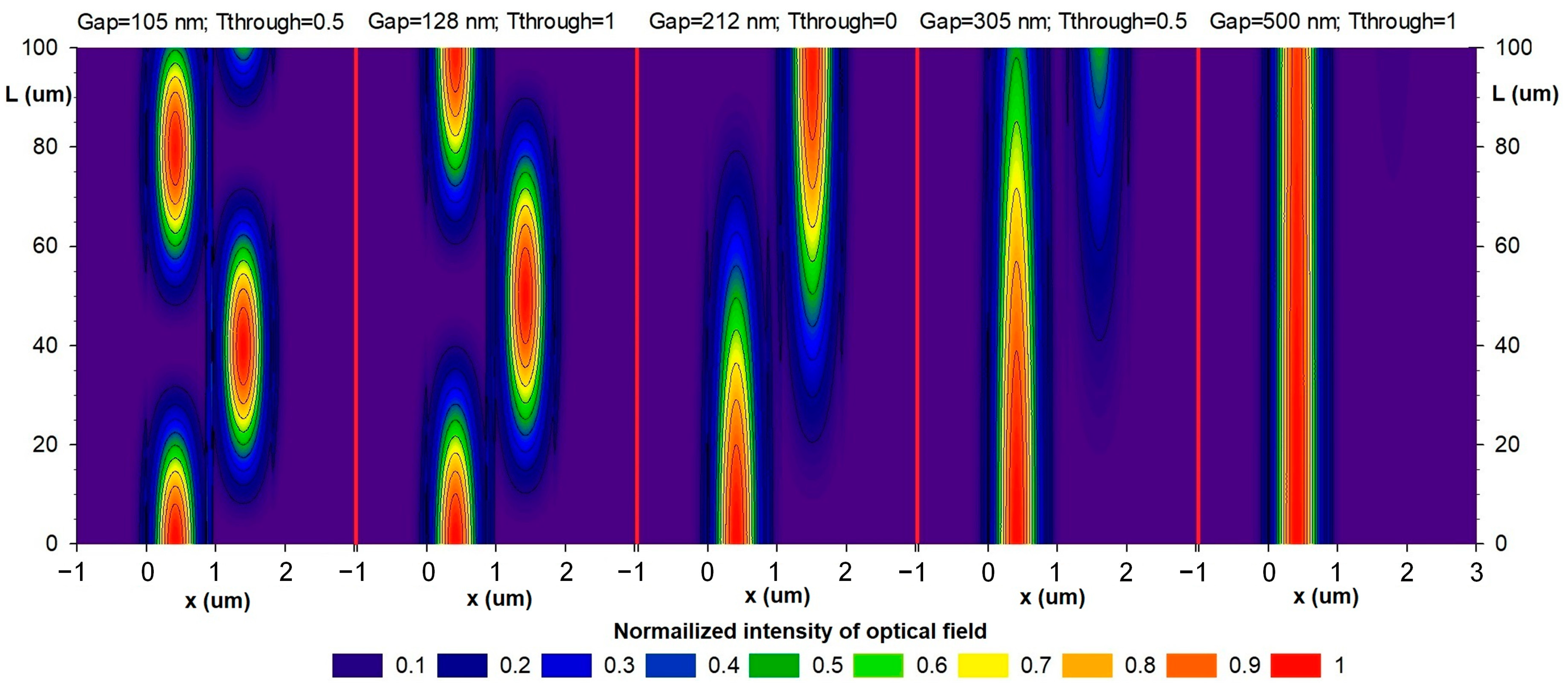
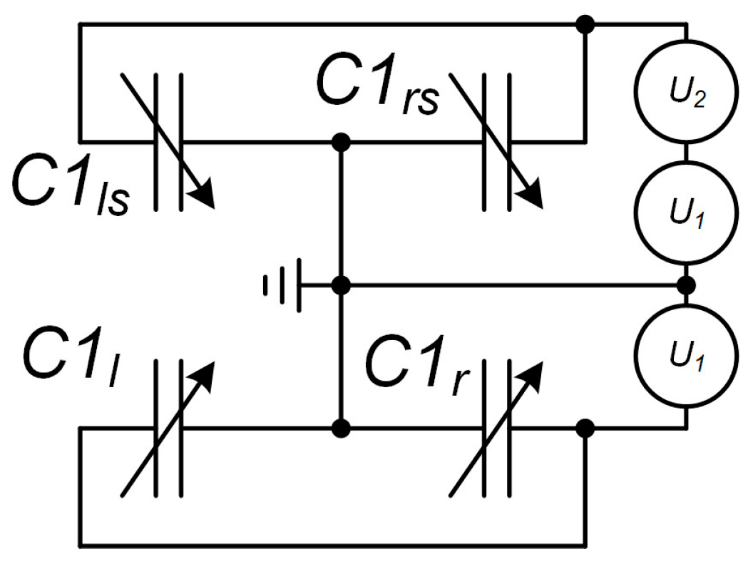
3. Optical Measuring Transducers
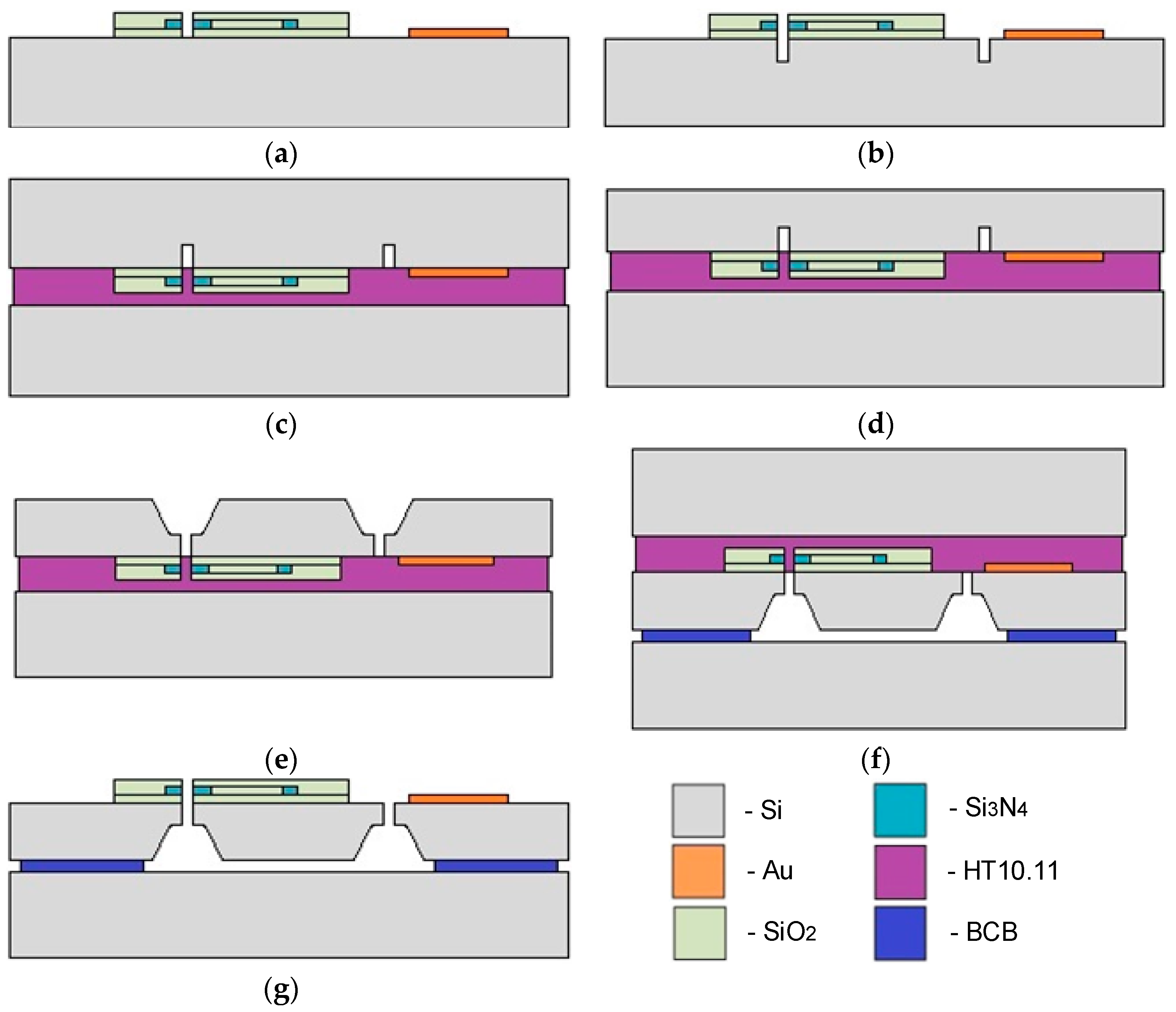
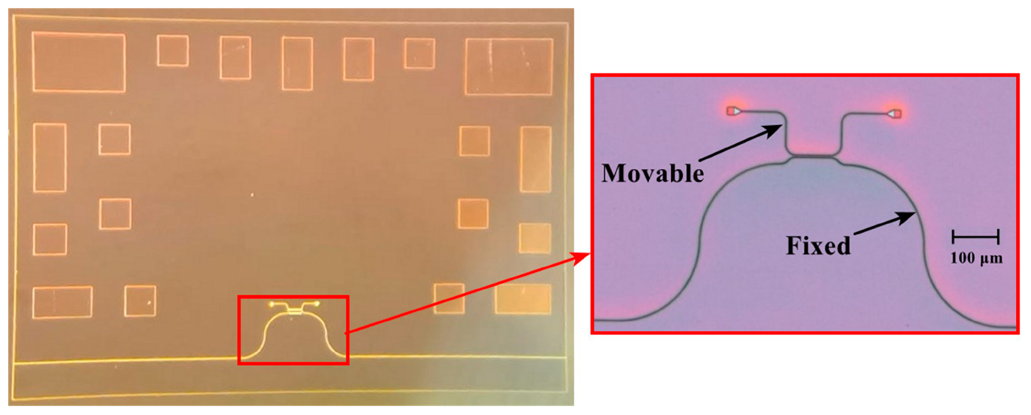
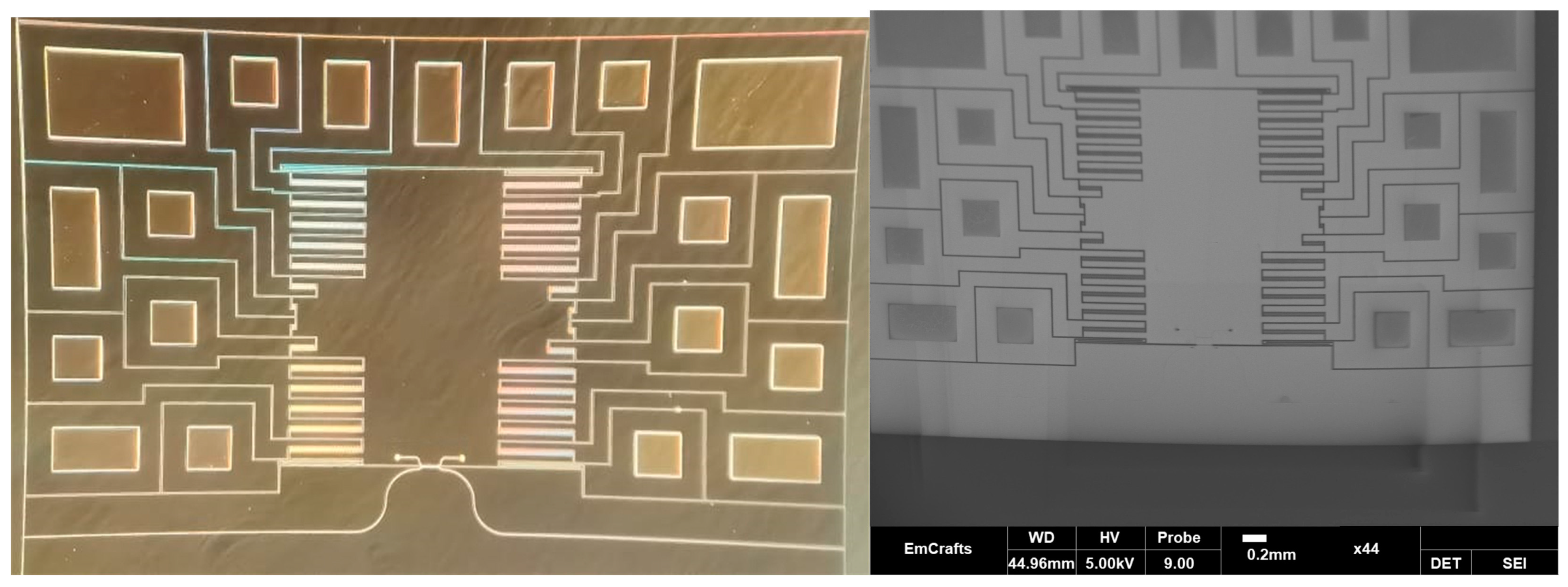
4. Fabrication of the Accelerometer
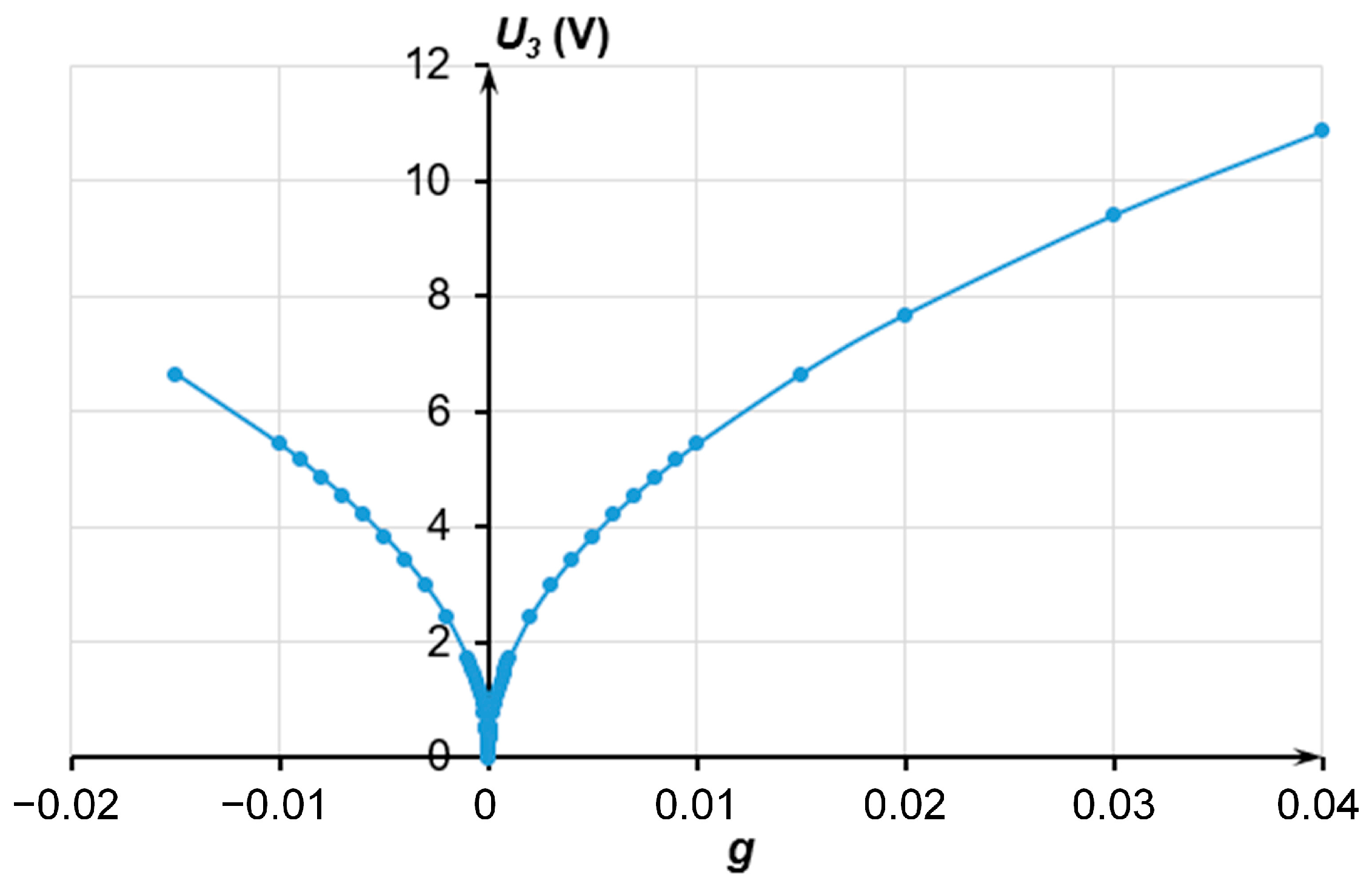
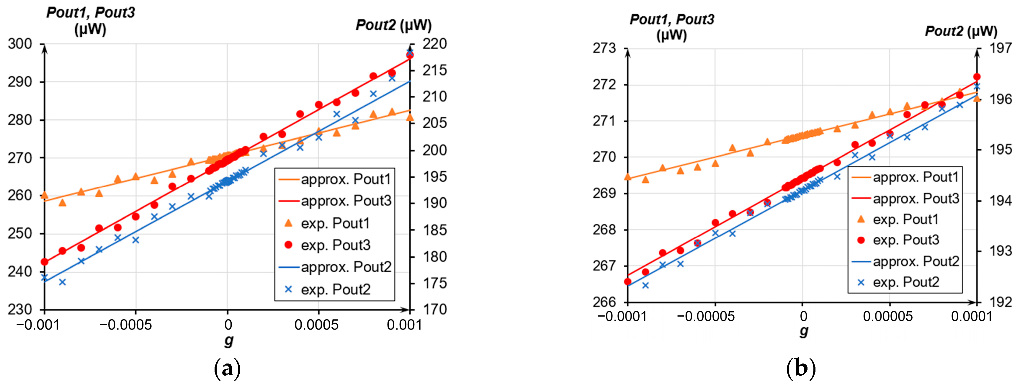
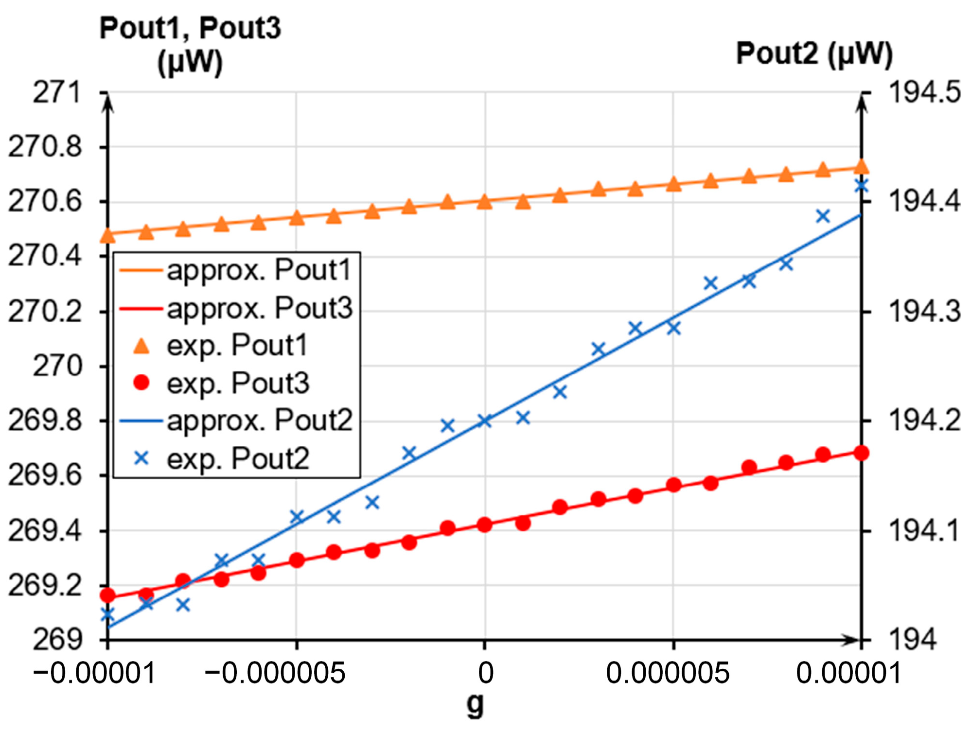
5. Experimental
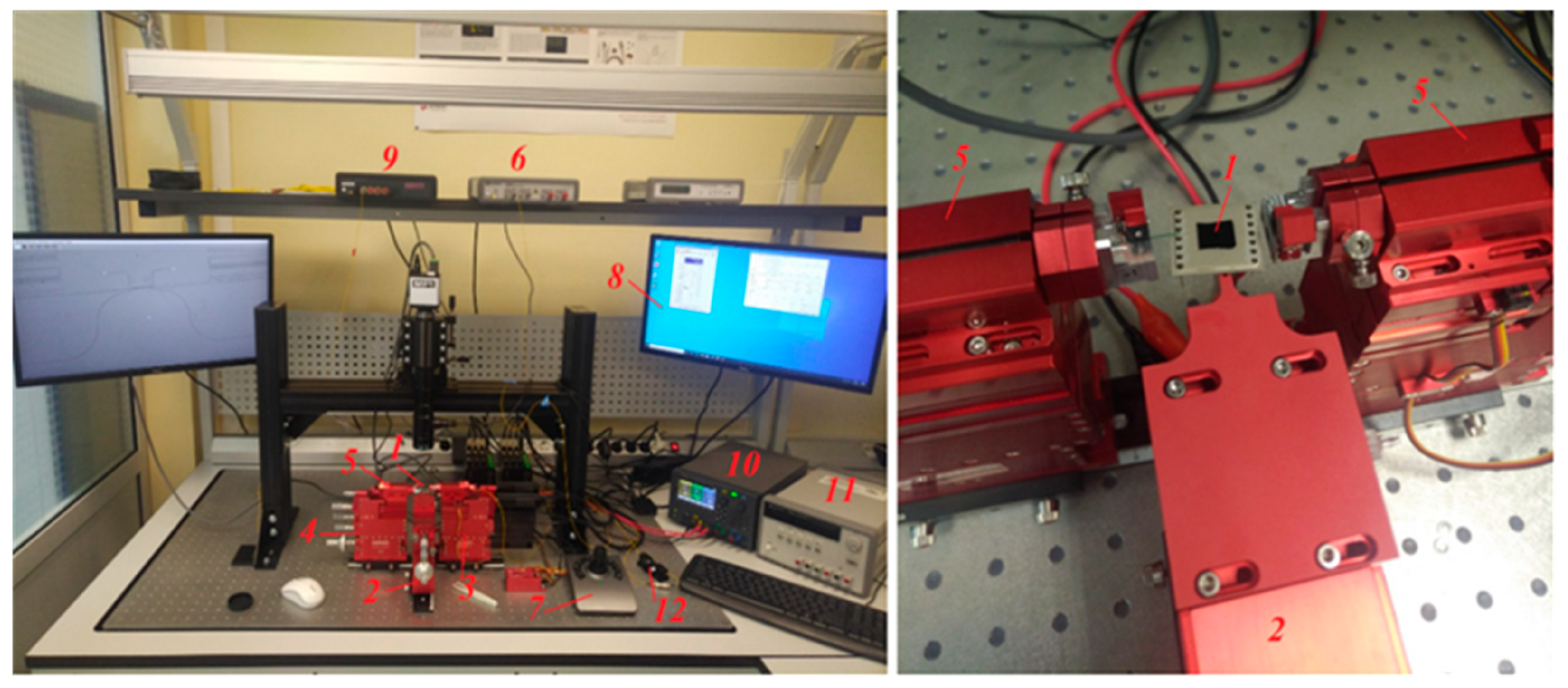
5.1. Setup
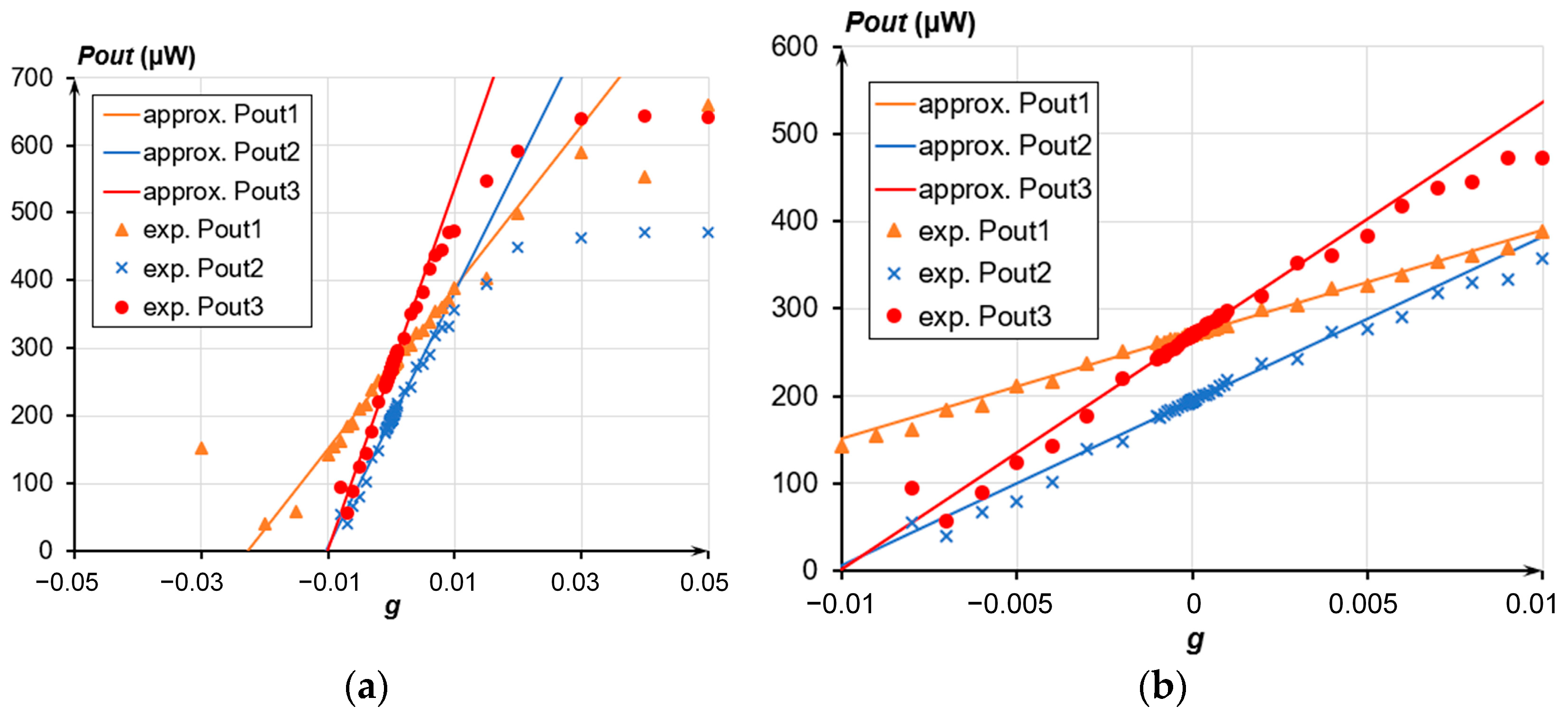
5.2. Testing of the Accelerometer
6. Conclusions
Author Contributions
Funding
Institutional Review Board Statement
Informed Consent Statement
Data Availability Statement
Conflicts of Interest
References
- Krishnan, G.; Kshirsagar, C.U.; Ananthasuresh, G.K.; Bhat, N. Micromachined High-Resolution Accelerometers. J. Indian Inst. Sci. 2007, 87, 333–360. [Google Scholar]
- Liu, H. Design, Fabrication and Characterization of a MEMS Gravity Gradiometer; Imperial College London: London, UK, 2016. [Google Scholar] [CrossRef]
- D’Alessandro, A.; Scudero, S.; Vitale, G. A Review of the Capacitive MEMS for Seismology. Sensors 2019, 19, 3093. [Google Scholar] [CrossRef] [PubMed]
- Lu, Q.; Wang, Y.; Wang, X.; Yao, Y.; Wang, X.; Huang, W. Review of Micromachined Optical Accelerometers: From mg to Sub-μg. Opto-Electron. Adv. 2021, 4, 200045. [Google Scholar] [CrossRef]
- Narasimhan, V.; Li, H.; Jianmin, M. Micromachined High-g Accelerometers: A Review. J. Micromech. Microeng. 2015, 25, 033001. [Google Scholar] [CrossRef]
- Elies, S. Performance Analysis of Commercial Accelerometers: A Parameter Review. Sens. Transducers 2015, 193, 179. [Google Scholar]
- Zachäus, C.; Müller, B.; Meyer, G. (Eds.) Advanced Microsystems for Automotive Applications 2017: Smart Systems Transforming the Automobile; Lecture Notes in Mobility; Springer International Publishing: Cham, Switzerland, 2018; ISBN 978-3-319-66971-7. [Google Scholar]
- Yazdi, N.; Ayazi, F.; Najafi, K. Micromachined Inertial Sensors. Proc. IEEE 1998, 86, 1640–1659. [Google Scholar] [CrossRef]
- Xin, C.; Zhang, Z.; Wang, X.; Fan, C.; Li, M. Ultracompact Single-Layer Optical MEMS Accelerometer Based on Evanescent Coupling through Silicon Nanowaveguides. Sci. Rep. 2022, 12, 21697. [Google Scholar] [CrossRef]
- Li, H.; Deng, K.; Gao, S.; Feng, L. Design of Closed-Loop Parameters with High Dynamic Performance for Micro-Grating Accelerometer. IEEE Access 2019, 7, 151939–151947. [Google Scholar] [CrossRef]
- Wang, Q.; Liu, H.F.; Tu, L.C. High-Precision MEMS Inertial Sensors for Geophysical Applications. Navig. Control 2018, 17. [Google Scholar]
- Wang, S.; Wei, X.; Zhao, Y.; Jiang, Z.; Shen, Y. A MEMS Resonant Accelerometer for Low-Frequency Vibration Detection. Sens. Actuators A Phys. 2018, 283, 151–158. [Google Scholar] [CrossRef]
- Gautam, A.; Kumar, A. Microseismic Wave Detection in Coal Mines Using Differential Optical Power Measurement. Opt. Eng. 2019, 58, 1. [Google Scholar] [CrossRef]
- Krause, A.G.; Winger, M.; Blasius, T.D.; Lin, Q.; Painter, O. A High-Resolution Microchip Optomechanical Accelerometer. Nat. Photon. 2012, 6, 768–772. [Google Scholar] [CrossRef]
- Yao, B.; Feng, L.; Wang, X.; Liu, M.; Zhou, Z.; Liu, W. Design of Out-of-Plane MOEMS Accelerometer with Subwavelength Gratings. IEEE Photon. Technol. Lett. 2014, 26, 1027–1030. [Google Scholar] [CrossRef]
- Loh, N.C.; Schmidt, M.A.; Manalis, S.R. Sub-10 Cm/Sup 3/Interferometric Accelerometer with Nano-g Resolution. J. Microelectromech. Syst. 2002, 11, 182–187. [Google Scholar] [CrossRef]
- Weng, Y.; Qiao, X.; Guo, T.; Hu, M.; Feng, Z.; Wang, R.; Zhang, J. A Robust and Compact Fiber Bragg Grating Vibration Sensor for Seismic Measurement. IEEE Sens. J. 2012, 12, 800–804. [Google Scholar] [CrossRef]
- Huang, Y.; Guo, T.; Lu, C.; Tam, H.-Y. VCSEL-Based Tilted Fiber Grating Vibration Sensing System. IEEE Photon. Technol. Lett. 2010, 22, 1235–1237. [Google Scholar] [CrossRef]
- Stephens, M. A Sensitive Interferometric Accelerometer. Rev. Sci. Instrum. 1993, 64, 2612–2614. [Google Scholar] [CrossRef]
- Yu, B.; Wang, A.; Pickrell, G.R. Analysis of Fiber Fabry-Pe/Spl Acute/Rot Interferometric Sensors Using Low-Coherence Light Sources. J. Light. Technol. 2006, 24, 1758–1767. [Google Scholar] [CrossRef]
- Liu, C.-H.; Kenny, T.W. A High-Precision, Wide-Bandwidth Micromachined Tunneling Accelerometer. J. Microelectromechan. Syst. 2001, 10, 425–433. [Google Scholar] [CrossRef]
- Feng, Y.; Yang, W.; Zou, X. Design and Simulation Study of an Optical Mode-Localized MEMS Accelerometer. Micromachines 2022, 14, 39. [Google Scholar] [CrossRef] [PubMed]
- Liu, Y.; Li, F.; Huang, W. Perovskite Micro-/Nanoarchitecture for Photonic Applications. Matter 2023, 6, 3165–3219. [Google Scholar] [CrossRef]
- Yao, Y.; Pan, D.; Wang, J.; Dong, T.; Guo, J.; Wang, C.; Geng, A.; Fang, W.; Lu, Q. Design and Modification of a High-Resolution Optical Interferometer Accelerometer. Sensors 2021, 21, 2070. [Google Scholar] [CrossRef]
- Mireles, J.; Sauceda, Á.; Jiménez, A.; Ramos, M.; Gonzalez-Landaeta, R. Design and Development of a MOEMS Accelerometer Using SOI Technology. Micromachines 2023, 14, 231. [Google Scholar] [CrossRef] [PubMed]
- Abozyd, S.; Toraya, A.; Gaber, N. Design and Modeling of Fiber-Free Optical MEMS Accelerometer Enabling 3D Measurements. Micromachines 2022, 13, 343. [Google Scholar] [CrossRef] [PubMed]
- Taghavi, M.; Latifi, H.; Parsanasab, G.M.; Abedi, A.; Nikbakht, H.; Poorghadiri, M.H. A Dual-Axis MOEMS Accelerometer. IEEE Sens. J. 2021, 21, 13156–13164. [Google Scholar] [CrossRef]
- Sun, P.; She, X.; Yao, J.; Chen, K.; Bi, R.; Wang, L.; Shu, X. Monolithic Integrated Micro-Opto-Electromechanical Accelerometer Based on Michelson Interferometer Structure. J. Light. Technol. 2022, 40, 4364–4372. [Google Scholar] [CrossRef]
- Chen, W.; Jin, L.; Wang, Z.; Peng, H.; Li, M. Design and Demonstration of an In-Plane Micro-Optical-Electro-Mechanical-System Accelerometer Based on Talbot Effect of Dual-Layer Gratings. Micromachines 2023, 14, 1301. [Google Scholar] [CrossRef] [PubMed]
- Gholamzadeh, R.; Gharooni, M.; Salarieh, H.; Akbari, J. Design and Fabrication of a Micro-Opto-Mechanical-Systems Accelerometer Based on Intensity Modulation of Light Fabricated by a Modified Deep-Reactive-Ion-Etching Process Using Silicon-on-Insulator Wafer. J. Vac. Sci. Technol. B 2022, 40, 043001. [Google Scholar] [CrossRef]
- Soltanian, E.; Jafari, K.; Abedi, K. A Novel Differential Optical MEMS Accelerometer Based on Intensity Modulation, Using an Optical Power Splitter. IEEE Sens. J. 2019, 19, 12024–12030. [Google Scholar] [CrossRef]
- Barbin, E.; Nesterenko, T.; Koleda, A.; Shesterikov, E.; Kulinich, I.; Kokolov, A. An Optical Measuring Transducer for a Micro-Opto-Electro-Mechanical Micro-g Accelerometer Based on the Optical Tunneling Effect. Micromachines 2023, 14, 802. [Google Scholar] [CrossRef] [PubMed]
- Jian, A.; Wei, C.; Guo, L.; Hu, J.; Tang, J.; Liu, J.; Zhang, X.; Sang, S. Theoretical Analysis of an Optical Accelerometer Based on Resonant Optical Tunneling Effect. Sensors 2017, 17, 389. [Google Scholar] [CrossRef] [PubMed]
- Barbin, E.S.; Nesterenko, T.G.; Koleda, A.N.; Shesterikov, E.V.; Kulinich, I.V.; Sheyerman, F.I. Estimating the Sensitivity of Microoptoelectromechanical Micro-g Accelerometer. In Proceedings of the 2022 IEEE 23rd International Conference of Young Professionals in Electron Devices and Materials (EDM), Altai, Russian, 30 June–4 July 2022; pp. 52–56. [Google Scholar]
- Barbin, E.S.; Nesterenko, T.G.; Koleda, A.N.; Shesterikov, E.V.; Kulinich, I.V.; Kokolov, A.A. A System for Positioning an Optical Tunnel Measuring Transducer of a Microoptoelectromechanical Micro-g Accelerometer. In Proceedings of the 2022 IEEE 23rd International Conference of Young Professionals in Electron Devices and Materials (EDM), Altai, Russian, 30 June 2022; pp. 42–47. [Google Scholar] [CrossRef]
- Acar, C.; Shkel, A.M. MEMS Vibratory Gyroscopes: Structural Approaches to Improve Robustness; MEMS reference shelf; Springer: New York, NY, USA; London, UK, 2008; ISBN 978-0-387-09536-3. [Google Scholar]
- Chrostowski, L.; Hochberg, M. Silicon Photonics Design: From Devices to Systems, 1st ed.; Cambridge University Press: Cambridge, MA, USA, 2015; ISBN 978-1-107-08545-9. [Google Scholar]


| Device Type | Sensitivity | Eigenfrequency | Intrinsic Noise | Measuring Range | Bandwidth |
|---|---|---|---|---|---|
| Photonic-crystal nanocavity [14] | 10 µg Hz−1/2 | 20 kHz | - | - | 50 dB |
| Sub-wavelength gratings [15] | 2033 nm/g | 379 Hz | - | 0.12 g | - |
| Interferometric position sensor [16] | - | From 80 Hz to 1 kHz | 40 ng/rt Hz | - | 85 dB at 40 Hz |
| Fiber Bragg grating [17] | ~100 pm/g cross-axis anti-interference degree < 5% | (10–120) Hz | - | - | - |
| Fiber grating [18] | - | - | - | - | Up to 200 Hz |
| Electron tunneling transducers [21] | - | - | 20 ng/Hz | - | 5 Hz–1.5 kHz |
| Ring resonators [22] | 18.9/g | - | 4.874 μg | From −23.5 g to 29.4 g | - |
| Micro-grating-based [24] | 169 μm/g 60 V/g | - | 15 ng/√Hz for 1 Hz | - | - |
| Fabry–Pérot interferometer (FPI) [25] | (1.022–1.029) mV/(m/s2) | 1274 Hz | - | 7 g | - |
| Fiber-free optical [26] | 0.156 mA/g, resolution of 56.2 µG | - | - | - | |
| Fabry–Perot (FP) cavities [27] | X-axis—309 μg Y-axis—313 μg | X-axis—1382.5 Hz Y-axis—1398.6 Hz | - | 1 g | - |
| Michelson interferometer structure [28] | 3.638 nm/g | 1742.2 Hz | - | ±500 g | - |
| Talbot effect [29] | 0.14 μm/g 0.74 V/g | 1878.9 Hz | 2.0 mg | - | - |
| Intensity modulation of light [30] | 600 nm/g | 560 Hz | - | 3 g | - |
| Photonic crystal [31] | 0.0750 nm/g | 17.7 kHz | - | ±200 g | - |
| Optical tunneling effect [32] | (6.25 × 10⁶ m−1) | (10–200) Hz | - | - | - |
| Optical tunneling effect [33] | 9 pm/g | - | - | ±130 g | 0–1500 Hz |
| M, kg | 1.00 × 10⁻⁸ | 1.00 × 10⁻⁷ | 1.00 × 10⁻⁶ | 1.00 × 10⁻⁵ | |
|---|---|---|---|---|---|
| fy, Hz | fz, Hz | G, μm | |||
| 10 | 87.5 | 23,510 | 10,910 | 5060 | 2370 |
| 20 | 175 | 14,770 | 6860 | 3200 | 1505 |
| 50 | 437.5 | 8040 | 3760 | 1760 | 836 |
| 100 | 875 | 5094 | 2374 | 1111 | 539 |
| 200 | 1750.04 | 3210 | 1509 | 720.3 | 353.7 |
| M, kg | 1.00 × 10⁻⁸ | 1.00 × 10⁻⁷ | 1.00 × 10⁻⁶ | 1.00 × 10⁻⁵ | |
|---|---|---|---|---|---|
| fy, Hz | fz, Hz | Δz, μm | |||
| 10 | 87.5 | 32.8831 | 32.7483 | 32.5152 | 33.2363 |
| 20 | 175 | 8.16708 | 8.12145 | 8.20043 | 8.52342 |
| 50 | 437.5 | 1.3078 | 1.32746 | 1.35832 | 1.5075 |
| 100 | 875 | 0.3331137 | 0.333466 | 0.355366 | 0.440739 |
| 200 | 1750.04 | 0.0826125 | 0.085916 | 0.0983281 | 0.149845 |
Disclaimer/Publisher’s Note: The statements, opinions and data contained in all publications are solely those of the individual author(s) and contributor(s) and not of MDPI and/or the editor(s). MDPI and/or the editor(s) disclaim responsibility for any injury to people or property resulting from any ideas, methods, instructions or products referred to in the content. |
© 2024 by the authors. Licensee MDPI, Basel, Switzerland. This article is an open access article distributed under the terms and conditions of the Creative Commons Attribution (CC BY) license (https://creativecommons.org/licenses/by/4.0/).
Share and Cite
Barbin, E.; Nesterenko, T.; Koleda, A.; Shesterikov, E.; Kulinich, I.; Kokolov, A.; Perin, A. The Design, Modeling and Experimental Investigation of a Micro-G Microoptoelectromechanical Accelerometer with an Optical Tunneling Measuring Transducer. Sensors 2024, 24, 765. https://doi.org/10.3390/s24030765
Barbin E, Nesterenko T, Koleda A, Shesterikov E, Kulinich I, Kokolov A, Perin A. The Design, Modeling and Experimental Investigation of a Micro-G Microoptoelectromechanical Accelerometer with an Optical Tunneling Measuring Transducer. Sensors. 2024; 24(3):765. https://doi.org/10.3390/s24030765
Chicago/Turabian StyleBarbin, Evgenii, Tamara Nesterenko, Aleksej Koleda, Evgeniy Shesterikov, Ivan Kulinich, Andrey Kokolov, and Anton Perin. 2024. "The Design, Modeling and Experimental Investigation of a Micro-G Microoptoelectromechanical Accelerometer with an Optical Tunneling Measuring Transducer" Sensors 24, no. 3: 765. https://doi.org/10.3390/s24030765
APA StyleBarbin, E., Nesterenko, T., Koleda, A., Shesterikov, E., Kulinich, I., Kokolov, A., & Perin, A. (2024). The Design, Modeling and Experimental Investigation of a Micro-G Microoptoelectromechanical Accelerometer with an Optical Tunneling Measuring Transducer. Sensors, 24(3), 765. https://doi.org/10.3390/s24030765