3.1. Basic Parameter-Based Device Performance
The fabrication process of a CuO/ZnO heterojunction pyroelectric photodetector on an ITO glass substrate is illustrated in
Figure 1a.
Figure 1b,c present the top and side views of the CuO devices, respectively. The SEM images indicate that the crystal particles on the surface of the films prepared at room temperature are exceptionally small, with grain sizes in the nanometer scale. The demarcation lines between the p-CuO, n-ZnO, and AZO layers are distinct. The thicknesses measured are approximately 60 nm for the AZO film, 145 nm for the ZnO film, and 89 nm for the bottom CuO thin film. Additionally, AFM test images in
Supplementary Material Figure S20 present the surface heights and contact potentials of CuO, CuO-ZnO, and CuO-ZnO-AZO. It can be observed that the surface topography of the fabricated films is smooth, indicating improved surface growth.
Figure 1d presents the EDS spectral analysis of the device under basic parameters, which indicates that ZnO has the highest proportion, followed by CuO, and then AZO. This result is consistent with the layer thickness measurements obtained in
Figure 1c, further validating the accuracy and reliability of the data. The transmission spectrum of the whole device is shown in
Figure 1e, showing that the whole device exhibits high transmittance, ranging from approximately 40% to 70% across wavelengths spanning from about 450 nm to 800 nm. This indicates that the whole device has a low absorption in this wavelength range. The transmission spectrum of CuO/ZnO heterojunction produced by magnetron sputtering is consistent with the experimental findings [
8,
40,
41]. Finally,
Figure 1f presents the XRD images of the whole device, with the major orientations corresponding to the XRD peaks of ZnO and CuO as clearly labeled. These results indicate that the whole device exhibits distinctive peaks in the lattice plane families of (101) corresponding to the ZnO and (110) corresponding to the CuO. The deposition was conducted with a sputtering power of 100 W, a duration of 30 min, and an oxygen–argon ratio of 1:3 (JCPDS No. 05-0661, JCPDS No. 36-1451).
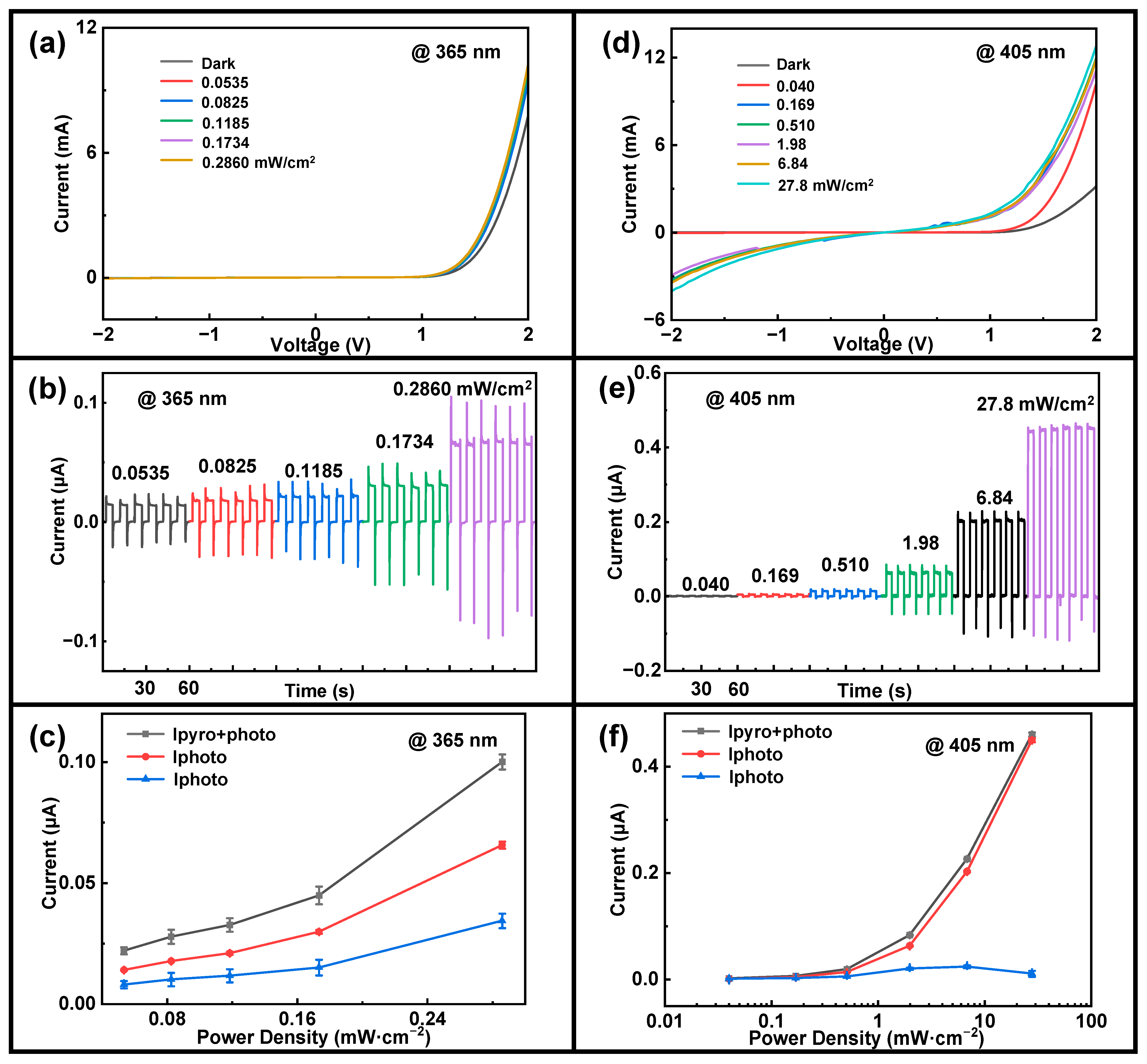
Figure 2a,d depict the current–voltage (I-V) characteristics of the p-CuO/n-ZnO heterojunction pyroelectric photodetector under 365 nm and 405 nm illumination. The device showed a strong photoresponse under forward bias, with the forward saturation current increasing consistently with light power density. The current at +2V bias increases dramatically from ~7.7 mA under dark conditions to ~10.2 mA under 0.286 mW/cm
2 365 nm UV illumination and from ~3.1 mA under dark conditions to ~12.7 mA under 27.8 mW/cm
2 405 nm illumination, respectively. These results demonstrate that the p-CuO/n-ZnO heterojunction exhibits good rectification behavior, suggesting effective electrical contact between CuO and ZnO.
Additionally, for a detailed transient characteristic analysis, the device was periodically illuminated by 365 nm and 405 nm lasers under zero bias, as shown in
Figure 2b,e. When a regularly switched laser illuminates the p-CuO/n-ZnO heterojunction pyroelectric photodetector, the device’s response demonstrates a classic four-step pyroelectric response [
42]. Initially, the photodetector resides in a dark state, characterized by a minimal dark current
within the device. Upon irradiation with laser light, a photovoltaic-induced current
is generated within the circuit. Additionally, the temperature of ZnO experiences an instantaneous increase, resulting in a positive rate of temperature change (
). The temperature variation generates a negative pyroelectric polarization potential at the p-CuO/n-ZnO heterojunction interface. This pyroelectric voltage
across the ZnO aligns with
, enabling the current to rapidly peak from the initial dark current, which includes both steady-state and pyroelectric photocurrents. Consequently,
continues to increase until it reaches the peak value
. Under continuous illumination, the temperature of ZnO gradually rises until it reaches saturation, at which point
. Then, the variations in temperature and the pyroelectric effect in ZnO progressively diminish, ultimately leaving only the steady-state photocurrent generated by photoexcitation. Consequently, the current decreases from its peak value
to
. When the illumination is abruptly turned off, the temperature of ZnO experiences an instantaneous decline, leading to a condition where
. This phenomenon induces a pyroelectric polarization potential that is contrary to the one generated during illumination, thereby limiting carrier transport within the heterojunction. As a result, the photocurrent experiences an immediate drop, leading to a reverse spike in
due to the opposing pyroelectric potential.
Figure S23a,b show the schematic energy band diagram of the device when light is turned on and off, clearly demonstrating the effects of the pyroelectric effect on the energy band diagram.
When the light source is turned off and the device reverts to its dark state, the temperature of ZnO returns to room temperature and stabilizes, at which point
. Consequently, the pyroelectric effect in ZnO diminishes once again, leading to a return of the current to its initial steady-state dark current
[
43]. The dark current level is on the order of 10
−9 A. In contrast to similar devices featuring an ITO-CuO-ZnO-ITO structure with a CuO sputtering power of 50 W, a sputtering time of 30 min, and an oxygen–argon ratio of 1:3, which typically display dark current levels on the order of 10
−3 A, this constitutes a significant enhancement in performance [
28]. The irradiation of the device was controlled by moving a black opaque cardboard, combined with a stopwatch to change the light on/off state every 5 s, achieving periodic irradiation of the device with a whole cycle of 60 s for each light power density. The power range of the 365 nm laser was measured to be 5.35 × 10
−2–2.86 × 10
−1 mW/cm
2, while the power range of the 405 nm laser was recorded as 4.0 × 10
−2–27.8 mW/cm
2. According to
Figure 2b,e, it is evident that at all light power densities, each light pulse exhibits a four-stage current response induced by the pyroelectric effect. The negative spike observed in the image, which represents the pyroelectric current, can be expressed as
, where
denotes the light absorption coefficient, A represents the electrode area of the device,
signifies the pyroelectric coefficient, and
is the rate at which the temperature of the device changes. It can be seen that I
pyro is proportional to
. In
Figure 2b,e, both the positive current spike I
pyro+photo and the negative current spike I
pyro exhibit an increase with rising light power density. This phenomenon occurs because, as illumination intensifies, the light power density escalates, thereby enhancing the laser’s heating capability on the device, which in turn increases
, leading to an increase in pyroelectric current intensity. For this detector under zero bias, under 365 nm wavelength laser irradiation, I
pyro+photo increases from 0.02199 μA (0.0536 mW/cm
2) to 0.10009 μA (0.286 mW/cm
2) with increasing laser power density, and
increases from 0.00797 μA (0.0536 mW/cm
2) to 0.03439 μA (0.286 mW/cm
2). Under 405 nm wavelength laser irradiation, I
pyro+photo also increases rapidly with increasing laser power density, from 0.00165 μA (0.04 mW/cm
2) to 0.46011 μA (27.8 mW/cm
2), and I
pyro increases from 8.04 × 10
−4 μA (0.04 mW/cm
2) to 0.03439 μA (27.8 mW/cm
2). Additionally, as demonstrated in
Figure S1a,b, the ratio of I
pyro/I
photo decreases with increasing light power density for a fixed laser wavelength. This decrease is more pronounced at 405 nm compared to 365 nm. As a consequence, the total current I
pyro+photo is mainly contributed by the photovoltaic effect.
To demonstrate the improvement in photodetection performance facilitated by the pyro-phototronic effect,
Figure 2c,f present the calculated and plotted variations of three distinct currents in relation to optical power density. The total photocurrent generated by the pyro-phototronic effect is denoted as I
pyro+photo, while I
photo represents the photocurrent produced via the traditional photovoltaic effect, and I
pyro corresponds to the photocurrent arising from the pyroelectric effect. As illustrated in
Figure 2c,f, under illumination from laser light sources of varying wavelengths and power densities, the pyro-phototronic effect enhances the photodetector’s current from I
photo to I
pyro+photo. As illumination intensity increases, I
pyro improves only slightly, while I
pyro+photo and I
photo improve significantly. Meanwhile, according to the formula for responsivity [
44].
, where
is the optical power density and S represents the effective area of the light spot, the unit of responsivity is mA/W.
Figure 3a,b illustrate the variations in responsivity,
and
, as a function of increasing optical power density. The results indicate that under irradiation with lasers at 365 nm and 405 nm, the responsivity diminishes as the optical power density increases. It is noteworthy that at each level of optical power density, the responsivity
is significantly higher than
due to the contribution of the pyroelectric effect.
In
Figure 3a, the responsivity at 365 nm exhibits a non-monotonic trend, initially decreasing and then increasing as the power density rises. This behavior results from the interplay between two competing mechanisms. At lower power densities, the responsivity decreases due to the saturation of photogenerated carriers, as increased light intensity causes a saturation effect that limits the photoresponse. However, as the power density further increases, the temperature gradient induced by higher light intensity enhances the pyroelectric effect, contributing additional photocurrent. This enhanced pyroelectric contribution leads to a subsequent increase in responsivity at higher power densities. In contrast,
Figure 3d shows a different trend for responsivity at 405 nm due to the less pronounced pyroelectric effect at this longer wavelength compared to 365 nm. The responsivity at 405 nm initially increases with power density, primarily due to higher photogeneration efficiency. At low power densities, increased light absorption generates a larger number of carriers, enhancing the responsivity. However, at higher power densities, carrier recombination effects become significant, reducing the number of free carriers available for conduction and leading to a decrease in responsivity.
Additionally, according to the formula for detectivity
of the photodetector [
43], under 365 nm and 405 nm lasers, calculated as
, where
is the dark current density
, and
is the charge quantity, the unit of detectivity is Jones. The relevant plots are presented in
Figure 3c,f. Detectivity is a crucial parameter for assessing the capability of a photodetector to identify weak light signals. It defines the minimum detectable signal by taking into account the dark current as the primary source of noise. From
Figure 3c,f, it is evident that detectivity exhibits a similar trend to responsivity. At each optical power density, the pyro-phototronic effect has brought dramatic improvements compared to the photovoltaic effect-induced R
photo and D*
photo. Under 365 nm laser, R has been improved from ~0.45 mA/W to ~0.64 mA/W (by averaging over all the power densities) and D from ~208 × 10
8 Jones to ~324 × 10
8 Jones (by averaging over all the power densities). For the 405 nm laser, R has been improved from ~0.063 mA/W to ~0.074 mA/W and D from ~27 × 10
8 Jones to ~33 × 10
8 Jones.
significantly exceeds
due to the pyro-phototronic effect. The calculation of the maximum gain in photodetector responsivity relative to light power density is presented herein,
, as depicted in
Figure 3b,e. It is evident that under exposure to a 365 nm laser at 8.25 × 10
−1 mW/cm
2,
exceeds
by a factor of 60, while exposure to a 405 nm laser at 4.0 × 10
−2 mW/cm
2 results in
exceeding
by a factor of 108.
In
Figure 3b, the responsivity gain at 365 nm follows a distinct pattern: it initially increases and then decreases with increasing power density. At lower power densities, the pyroelectric contribution to the total responsivity is relatively large compared to the baseline photoresponsivity, resulting in a higher gain. As the power density increases, the dominant contribution shifts from the pyroelectric effect to photogenerated carriers. Consequently, the relative enhancement provided by the pyroelectric effect diminishes, causing the overall gain to decrease. Under illumination at 405 nm, both ZnO and CuO are capable of generating electron–hole pairs that contribute to the photocurrent, resulting in a high maximum gain. Due to the significant absorption coefficient of ZnO in the ultraviolet region, whereas CuO exhibits minimal absorption of ultraviolet light for electron–hole pair generation, the maximum gain under 365 nm illumination is relatively low. The maximum gain in detectivity,
, calculated with varying light power density, is shown in
Figure S1b,d. It is evident that under both 365 nm and 405 nm laser illuminations, the trend aligns consistently with the maximum gain in responsivity, indicating that the pyroelectric effect holds significant potential for enhancing photodetector performance. Response time is also a crucial parameter of photodetectors. The response time is categorized into rise time and fall time. For the devices fabricated by us, the rise time refers to the period during which
of the device ascends from 10% to 90% when the external light is turned on. Fall time is the time when the device drops from 90% of the difference between
and reverse
to 10% when the external light is turned off.
3.2. Sputtering Power
To investigate the influence of the CuO layer in p-CuO/n-ZnO heterojunction pyroelectric photodetectors, different p-CuO thin films were deposited under various sputtering powers while keeping other conditions constant. The same transient response test was then conducted on the resulting photodetectors. Experiments were conducted using three sputtering powers (100 W, 120 W, and 140 W) for CuO deposition, maintaining consistent sputtering conditions otherwise.
The top SEM images in
Figure 4a,d depict CuO thin films on silicon wafers sputtered at 120 W and 140 W for 30 min, with an oxygen–argon ratio of 1:3. The CuO film at 120 W sputtering power is denser than the film at 140 W sputtering power. As the sputtering power is increased, distinct variations in the surface morphology of the deposited films are observed.
Figure S6a,d show the cross-sectional SEM images of CuO films under 120 W and 140 W sputtering power. All cross-sectional SEM images show the well-sputtered CuO films, but the thickness of the films increases with increasing sputtering power.
Figure S6b,e show the EDS mappings of CuO films under 120 W and 140 W sputtering power. Combining the two XRD images of
Figure S6c,f, we can see that the positions of the main peaks of CuO are similar under different sputtering powers, indicating that the crystalline phases of the films have not changed significantly and the characteristic crystalline phases of CuO are still preserved. The main diffraction peaks of the 120 W sample are relatively sharper, and the peak widths are narrower, indicating that the films are more crystallized under 120 W sputtering power.
Figure 4g presents the transmission spectra of CuO films at various sputtering powers. The data indicate a notable decrease in transmittance within the shorter wavelength range (300–500 nm) as the sputtering power increases. Furthermore, higher sputtering powers result in improved transmittance at higher wavelengths and reduced transmittance at lower wavelengths. Furthermore,
Figure 4g shows that the absorption edge of the CuO film sputtered at 140 W exhibits the slowest response, indicating the poorest crystallinity. Combining this with the SEM images, it can be concluded that higher sputtering power increases the thickness, thereby affecting the light transmission properties in different wavelength ranges.
For the p-CuO/n-ZnO heterojunction pyroelectric photodetectors under sputtering powers of 120 W and 140 W, the I-V characteristics of the detector under 120 W sputtering power under 365 nm and 405 nm illumination were first tested and plotted in
Figure S2a,d. The device demonstrates favorable forward bias photoresponse characteristics, with the forward saturation current progressively increasing with rising light power density at constant forward bias voltage. The I-t characteristics under both illuminations are presented in
Figure S2b,e. These measurements were conducted under the same testing conditions as those applied to the device at 100 W sputtering power. The device demonstrates the four-stage current response due to the pyroelectric photoelectric coupling effect in each cycle, indicating robust I-t characteristics. Furthermore, the photocurrent response gradually increases with the increase of light intensity. The I-V characteristics under 365 nm and 405 nm laser illumination at 120 W sputtering power are also measured and plotted in
Figure S2a,d, showing that the device still has good forward saturation photocurrent at this sputtering power, while the reverse photocurrent is close to 0.
Figure S2c,f shows the variation of current with light power density under the two types of laser illumination.
Figure S3 shows the maximum responsivity gain, detectivity, and maximum detectivity gain of the device at 120 W sputtering power under periodic irradiation of the two types of lasers as a function of light power density. The current–voltage, current–time, and current–light power density plots of the detector under 365 nm and 405 nm laser illumination at 140 W sputtering power are shown in
Figure S4. The maximum responsivity gain, detectivity, and maximum detectivity gain under the two types of illumination are shown in
Figure S5. Through comprehensive comparison, we found that whether the device is fabricated under 120 W or 140 W sputtering power, it can be seen from
Figure S2a,d that it has good rectification behavior, and it can be seen that the pyro-phototronic effect has a significant improvement on the devices’ performances.
Figure 4b,c show the responsivity of the photodetector under 365 nm and 405 nm lasers at sputtering powers of 120 W and 140 W, respectively. Under both laser wavelengths, it can be observed that
and
decrease with increasing light intensity. However, at each light power density, the responsivity
is higher than
due to the pyroelectric effect. For the sputtering power of 120 W, R has been improved from ~0.7 mA/W to ~1.8 mA/W under 365 nm laser and from ~0.13 mA/W to ~0.18 mA/W under 405 nm laser. For the sputtering power of 140 W, R has been improved from ~0.09 mA/W to ~0.19 mA/W under a 365 nm laser and from ~0.039 mA/W to ~0.044 mA/W under a 405 nm laser. Hence, we can see that at 120 W sputtering power, the pyroelectric current has the largest overall current enhancement effect on the device, and the pyro-phototronic effect is the most significant.
Figure 4h,i illustrate the variation in responsivity
and
as a function of sputtering power under 365 nm and 405 nm lasers, respectively. The photodetector exhibits the highest responsivity at a sputtering power of 120 W for both laser wavelengths, indicating optimal performance at this power level.
The comparison of response times under different sputtering powers (100 W, 120 W, and 140 W) at two illumination wavelengths is presented in
Figures S21a,d and S22a,d. At the lower sputtering power of 100 W, the side-view SEM image in
Figure 1c reveals insufficient growth of the CuO thin film, resulting in a thin, non-uniform layer with poor surface coverage and inadequate thickness. This observation is further supported by the AFM images in
Figure S20, which compare the bottom CuO thin films with CuO/ZnO and CuO-ZnO-AZO heterojunction devices. The CuO film exhibits a surface roughness of approximately 10 nm, characterized by uneven surfaces and distinct, isolated grain structures. In contrast, increasing the sputtering power to 140 W significantly enhances the CuO film’s thickness, as shown in
Figure S6. However, higher sputtering power introduces excessive defects and internal stress [
45,
46,
47,
48]. These effects are evident in the device’s performance, particularly in the prolonged response times observed at higher sputtering power, as shown in
Figures S21 and S22. The side-view SEM image in
Figure S6 indicates that the CuO film thickness increases by approximately 20 nm compared to that at 120 W. This increased thickness hinders the transport and separation of photogenerated carriers, thereby reducing the device’s responsivity to some degree.
Combining the obtained characterization results and the test analysis of the device under two lasers, the sputtering power of 120 W was identified as optimal for the p-CuO device. Subsequent experiments were conducted using this optimized sputtering power to ensure enhanced device performance.
3.3. Sputtering Time
The sputtering power was fixed at 120 W. Experiments were then performed for four different sputtering times (15 min, 30 min, 45 min, and 60 min) with all other conditions unchanged.
Figure 5a,d,g, respectively, show the top SEM images of CuO films deposited on silicon wafers with sputtering times of 15 min, 45 min, and 60 min. It can be observed that as the sputtering time increases, the surface of the obtained films becomes rougher. The CuO film sputtered for 15 min is denser compared to the films obtained with other sputtering times.
Figure S13 shows the cross-sectional SEM images, EDS mappings, and XRD images of CuO films sputtered on silicon wafers for 15 min, 45 min, and 60 min. The cross-sectional SEM images reveal that while the CuO film’s thickness increases with sputtering time, the growth becomes increasingly disordered with extended deposition duration. Thinner films demonstrate greater uniformity and fewer structural defects. In contrast, extended sputtering times facilitate the formation of columnar structures or larger grains [
48], which could adversely impact carrier transport and lower device responsivity. The EDS mappings further support these observations, indicating that the sample deposited for 15 min exhibits the most uniform distribution of Cu and O, suggesting better stoichiometric control and consistent film coverage. In contrast, longer sputtering times lead to material inconsistencies and aggregation, with evidence of cluster formation in the EDS images. These findings are further supported by the XRD patterns. The 15-min sample displays sharp, well-defined peaks, reflecting superior crystallinity. In comparison, the 45-min and 60-min samples show broader peaks and increased background noise, indicating diminished crystallinity and the presence of amorphous or polycrystalline phases caused by excessive deposition.
Figure 5j shows the transmission spectra of CuO films for different sputtering times. For shorter sputtering times (15 min and 30 min), the transmittance increases rapidly. However, for longer sputtering times (45 min and 60 min), the increase in transmittance is more significant. This indicates that longer sputtering times may increase the film density, leading to higher transmittance. It can be seen that at the sputtering time of 15 min, the absorption edge of the CuO film is the sharpest, indicating that the film has the best crystallinity at this sputtering time.
Figures S7, S9, and S11 show the current–voltage (I-V) curves, current–time (I-t) curves, and current–optical power density (I-P) curves of devices at two light wavelengths under sputtering power of 120 W and an oxygen–argon ratio of 1:3, with sputtering times of 15 min, 45 min, and 60 min, respectively. It can be observed that all the devices fabricated at different sputtering times exhibit good rectification characteristics, with current increasing with optical power density under forward bias and approaching zero under reverse bias. At zero bias, all the devices show a four-stage current response under periodic light conditions. Additionally, as optical power density increases, both I
pyro+photo and I
photo increase significantly, while I
pyro remains smaller. This suggests that the photovoltaic current still makes a significant contribution to the total current, which is consistent with our previous findings.
Figure 5b,e,h present the responsivity,
and
, of photodetectors under 365 nm laser illumination for varying sputtering durations. It is evident that the responsivity generally decreases with increasing light power density, and the pyroelectric effect results in
being higher than
. For sputtering time of 15 min, R has been improved from ~0.54 mA/W to ~1.55 mA/W.
Figure 5c,f,i present the responsivity
and
of photodetectors exposed to a 405 nm laser for various sputtering durations. The results are consistent with those obtained under a 365 nm laser, reinforcing the conclusion that the pyroelectric effect enhances device responsivity. For sputtering time of 15 min, R has been improved from ~0.23 mA/W to ~0.38 mA/W. It is very clear that the device response is maximum at 15 min sputtering time.
Figure 5k,l illustrate the changes in responsivity
and
under 365 nm and 405 nm lasers with varying sputtering times. The data indicate that the photodetector achieves its maximum responsivity under the 405 nm laser at a sputtering time of 15 min.
Figures S8, S10, and S12 show the maximum responsivity gain–optical power density curves, detectivity-optical power density curves, and maximum gain detectivity–optical power density curves of devices at two light wavelengths under sputtering power of 120 W and an oxygen–argon ratio of 1:3, with sputtering times of 15 min, 45 min, and 60 min, respectively. It can be seen that the R and D of the device are relatively good, indicating the good electrical characteristics of the device. As the optical power density increases, the Ipyro also gradually increases, and the overall response contribution in the device also gradually increases. The comparison of response times under different sputtering times at two illumination wavelengths is presented in
Figures S21b,e, and S22b,e. The EDS mapping of the 15-min sample shows a more uniform Cu and O distribution, indicating better stoichiometric control. For longer sputtering times, the resulting films are thicker, with increased structural irregularities and higher defect density. These issues lead to increased scattering and slower response times, varying sputtering durations.
Therefore, combining the obtained characterization results and the test analysis of the device under two lasers, we conclude that a 15-min sputtering time yields the highest-quality CuO thin film, characterized by minimized structural defects, uniform coverage, and enhanced crystallinity.
3.4. Sputtering Oxygen–Argon Ratio
Using a sputtering power of 120 W and a sputtering time of 15 min, experiments were next conducted with three different oxygen–argon ratios: pure Ar, an oxygen–argon ratio of 1:1, and an oxygen–argon ratio of 1:3.
Figure 6a,d shows the SEM images of CuO films deposited on silicon wafers at a fixed sputtering power of 120 W and a sputtering time of 15 min, under pure Ar and an oxygen–argon ratio of 1:1, respectively.
Figure S18 shows the cross-sectional SEM images, EDS mappings, and XRD images of CuO films sputtered on silicon wafers for three different oxygen–argon ratios. It can be observed that in a pure argon environment, the surface crystal particles are dense and uniformly distributed, with higher roughness. When the oxygen–argon ratio is 1:1, the number of surface crystal particles decreases compared to a pure argon environment, resulting in a sparser distribution and a smoother surface. At an oxygen–argon ratio of 1:3, the number of surface crystal particles decreases further, leading to a more uniform distribution and an even smoother surface. Thus, different gas environments significantly impact the surface morphology of the material. Increasing the oxygen proportion reduces surface particle density and surface roughness. In a pure argon environment, deposited CuO’s surfaces contain dense and rough crystal particles. However, as the oxygen proportion increases, the surface crystal particle density decreases, resulting in a smoother surface. Oxygen effectively inhibits excessive particle growth to a certain extent. The CuO film grown under an oxygen–argon ratio of 1:3 exhibits a moderate and uniform thickness, in contrast to the excessively thick film obtained under pure Ar and the overly thin film grown with an oxygen–argon ratio of 1:1. This moderate thickness ensures optimal film growth and uniformity, while excessively thick films suffer from poor crystallinity and internal stress [
47], and overly thin films result in incomplete coverage and reduced quality. EDS mapping results further demonstrate that the oxygen–argon ratio of 1:3 condition yields the most homogeneous distribution of Cu and O, unlike the other conditions, which exhibit either oxygen deficiencies or non-uniform elemental distributions that compromise film integrity. XRD patterns confirm these findings, revealing sharp and well-defined peaks for the oxygen–argon ratio of 1:3, indicative of improved crystallinity. In comparison, films grown under pure Ar exhibit poor crystalline quality or non-stoichiometric phases due to insufficient oxygen supply. Similarly, the oxygen–argon ratio of 1:1 condition leads to suboptimal stoichiometry and crystallinity, attributed to an imbalance in the gas ratio. The response time measurements further confirm that the oxygen–argon ratio of 1:3 condition results in the fastest response, aligning with the superior film quality observed in the SEM and EDS analyses.
Figure 6g illustrates the transmittance spectra of CuO films under varying oxygen–argon sputtering ratios. It is evident that transmittance increases with wavelength across all curves. In the shorter wavelength range (from 300 nm to 500 nm), transmittance remains relatively low, with noticeable differences among different oxygen–argon ratios. Conversely, in the longer wavelength range (from 500 nm to 800 nm), transmittance shows a gradual increase, with values for different oxygen–argon ratios tending to converge. The transmittance is highest in a pure argon environment, indicating that the material’s transmittance performance is best without oxygen. The introduction of oxygen reduces the transmittance of the material, and the transmittance is lowest in the oxygen–argon ratio of 1:3 environment, indicating that a high oxygen ratio has a more significant negative impact on transmittance performance. Regardless of the gas environment, transmittance increases with wavelength, but the introduction of oxygen overall lowers the transmittance.
Figures S14 and S16 present the current–voltage, current–time, and current–light power density graphs of devices sputtered at 120 W for 15 min under pure argon and an oxygen–argon ratio of 1:1, respectively, at two wavelengths. It can be seen that the rectification characteristics of the devices are very different between the pure Ar and the oxygen–argon ratio of 1:1 and not as good as the devices fabricated in the oxygen–argon ratio of 1:3. When periodically illuminated, the four-stage response is still exhibited at zero bias, and it can be seen that the pyroelectric still has an enhancing effect on its light response. Similar to the previous conclusion, as the optical power density on the surface of the device increases, I
pyro+photo increases, and I
photo occupies the main contribution.
Figure 6b,e display the detector responsivity
and
under two different oxygen–argon ratios as the light intensity varies with a 365 nm wavelength laser. It is observed that as the power density of the 365 nm laser increases, the responsivity decreases, and the pyroelectric effect becomes notably significant. For different oxygen–argon ratios, R has been improved from ~0.23 mA/W to ~0.62 mA/W (pure Ar) and from ~0.98 mA/W to ~1.72 mA/W (oxygen–argon ratio of 1:1). It can be seen that the pyroelectric effect has a significant enhancement on the overall device responsivity.
Figure 6c,f depict the detector’s responsivity versus light intensity under 405 nm laser illumination. R has been improved from ~0.074 mA/W to ~0.12 mA/W (pure Ar) and from ~0.15 mA/W to ~0.24 mA/W (oxygen–argon ratio of 1:1). It is evident that the overall trend mirrors that observed under 365 nm laser illumination, thereby reinforcing our previous conclusions.
Figures S15 and S17 show the maximum responsivity gain–light power density, detectivity–light power density, and detectivity maximum gain–light power density graphs of devices sputtered at 120 W for 15 min under pure argon and an oxygen–argon ratio of 1:1, respectively, at two wavelengths. It can be observed that both I
photo and I
pyro within the device increase as the optical power density rises. However, the maximum gains in responsivity and detectivity decrease with increasing optical power density, suggesting that I
pyro increases at a slower rate compared to I
photo.
Figure 6h,i shows the changes in responsivity
and
at 365 nm and 405 nm lasers as the argon–oxygen ratio changes. Firstly, the addition of oxygen significantly enhances the device’s responsivity under both 365 nm and 405 nm lasers, especially when the argon–oxygen ratio is 1:1. Secondly, the responsivity at 365 nm reaches its peak at an oxygen–argon ratio of 1:1, while the responsivity at 405 nm gradually increases with the proportion of oxygen. Furthermore, the sum of the pyroelectric and photoelectric responses (
) under both laser conditions exceeds the individual photoelectric response (
), indicating a significant contribution of the pyroelectric effect to the overall response. The comparison of response times under different sputtering times at two illumination wavelengths is presented in
Figures S21c,f and S22c,f. Among the three oxygen–argon ratios tested, the ratio of 1:3 produced the best results. During the sputtering process, oxygen acts as an oxidizing agent. A higher oxygen ratio can result in the formation of a purer CuO film, reducing defects and impurities, which in turn enhances its photoelectric performance. Additionally, a higher oxygen ratio can produce finer and more uniform grains in the film, thereby increasing light absorption and carrier mobility. Furthermore, it can improve the interface quality by reducing interface defects and recombination centers, thereby enhancing carrier separation efficiency.
Therefore, combining the preliminary performance tests and the subsequent characterization results, we can obtain the best performance of the devices fabricated when the sputtered oxygen–argon ratio is 1:3.


