
Advances in Group-10 Transition Metal Dichalcogenide PdSe2-Based Photodetectors: Outlook and Perspectives


Abstract
1. Introduction
2. Figure of Merits and Types of PdSe2 Photodetectors
2.1. Figure of Merits (FoM) of PdSe2 Photodetectors
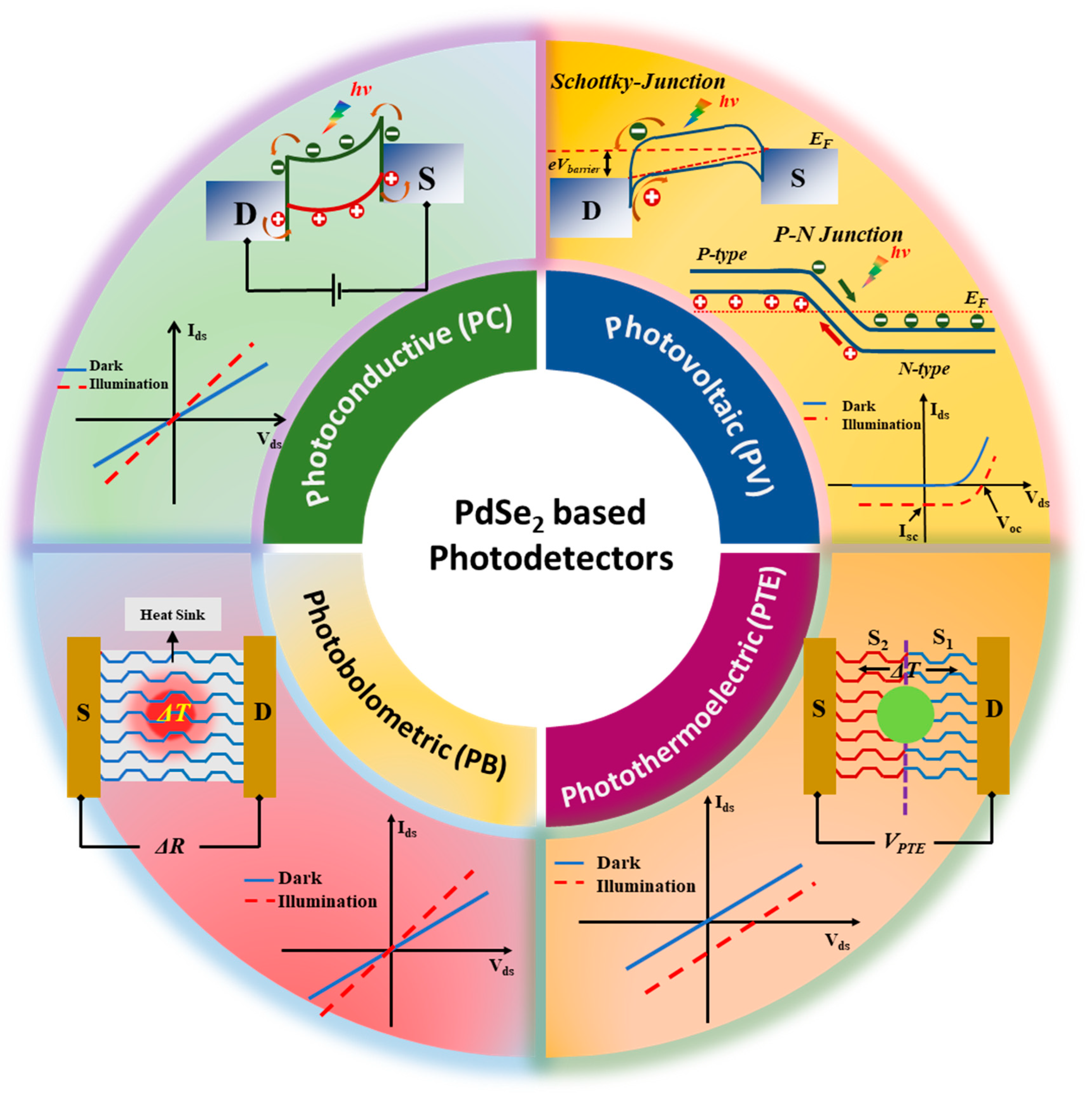
2.2. Types of PdSe2 Photodetectors
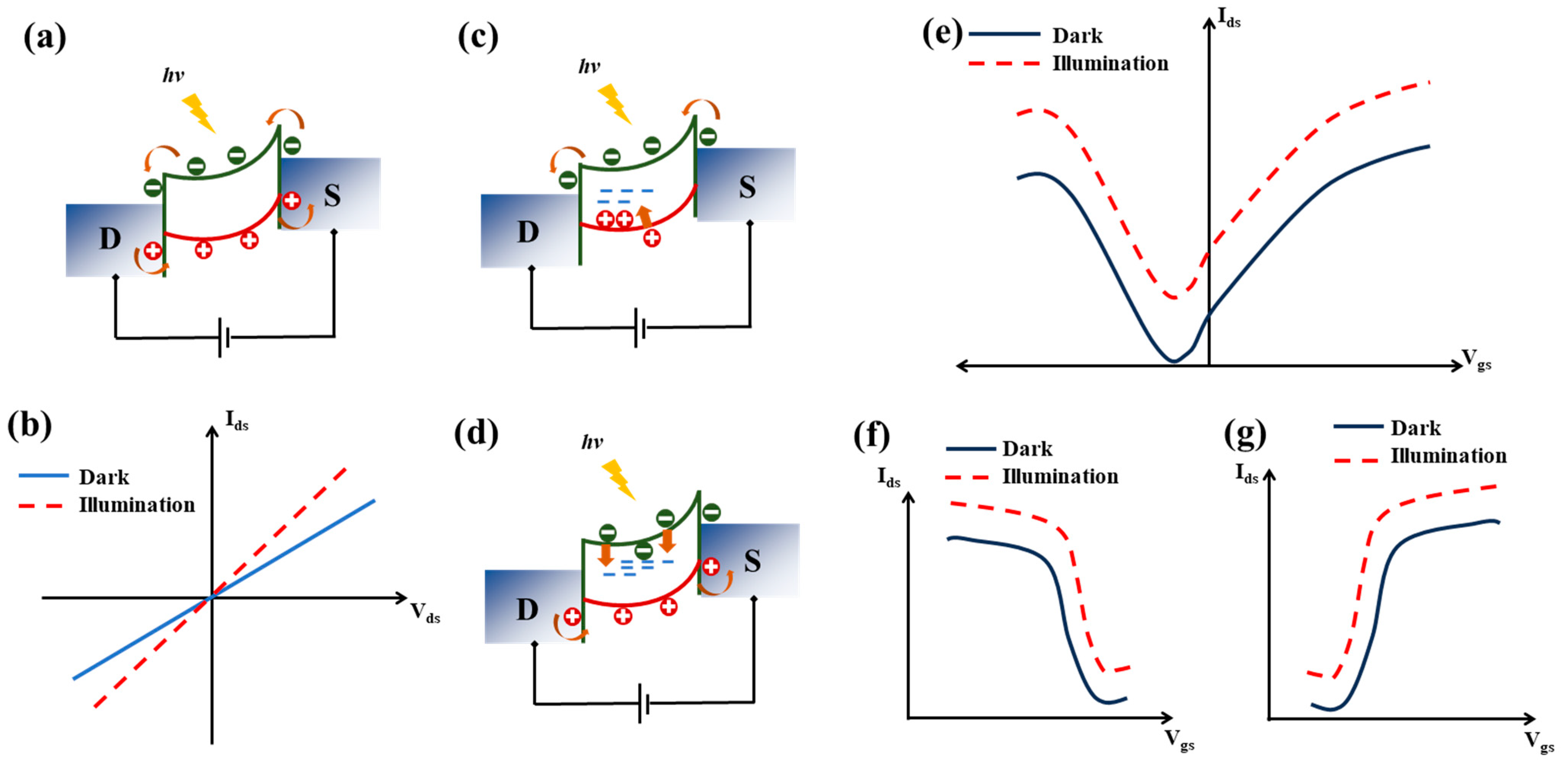
2.2.1. Photovoltaic Type Photodetectors
2.2.2. Photoconductive and Photo-Gated Photodetectors
2.2.3. Photothermoelectric (PTE) Photodetectors
2.2.4. Photobolometric Photodetectors
3. Properties of Group-10 TMDC PdSe2
3.1. Structural Characteristics
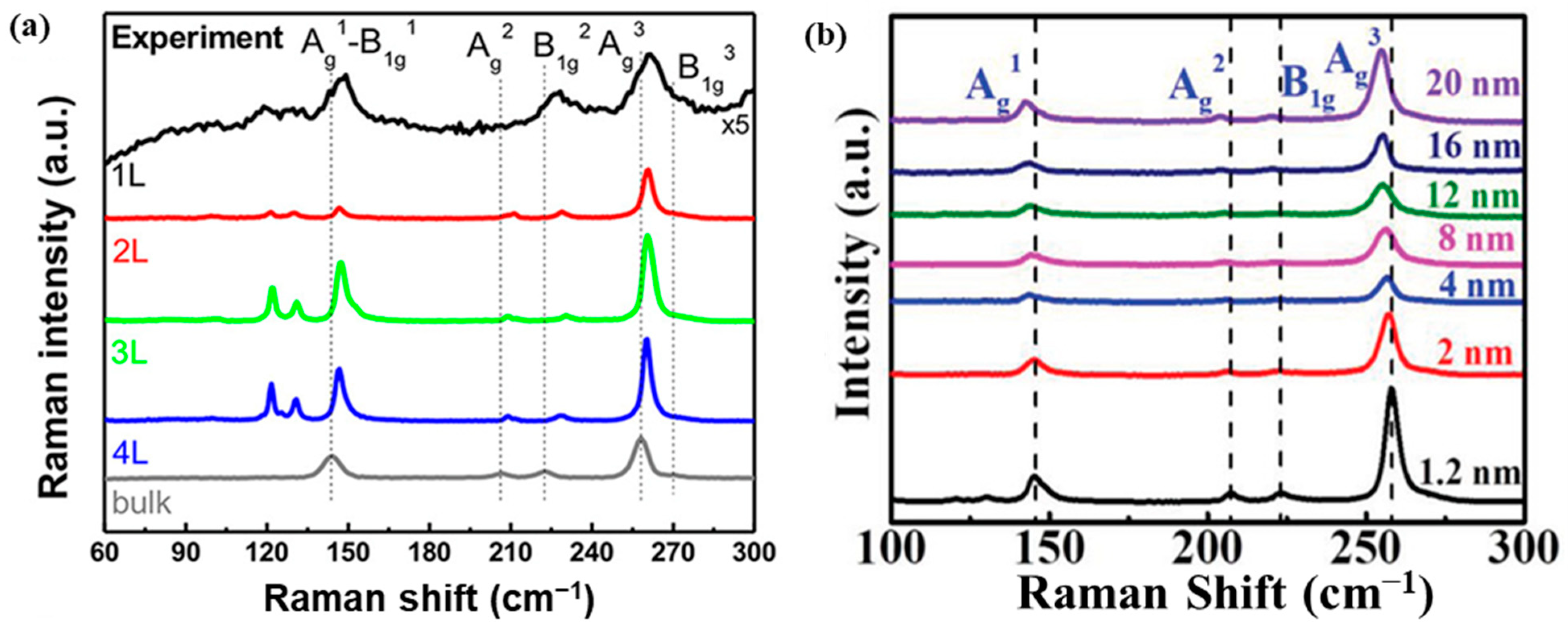
3.2. Raman Spectroscopic Characterization
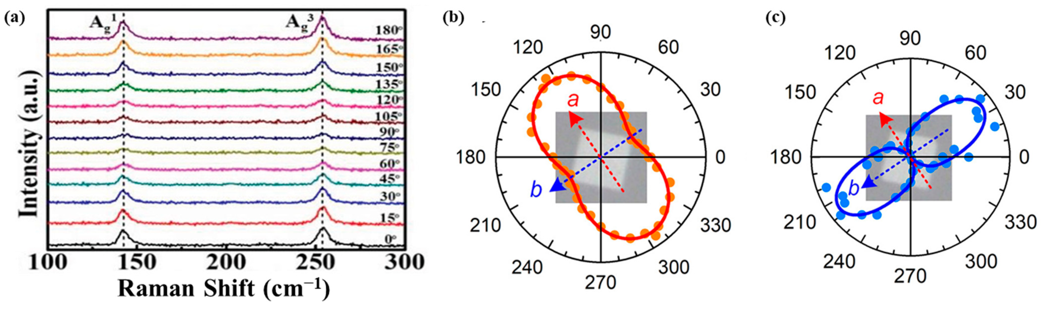
3.3. Anisotropic Response to Optical Stimulus
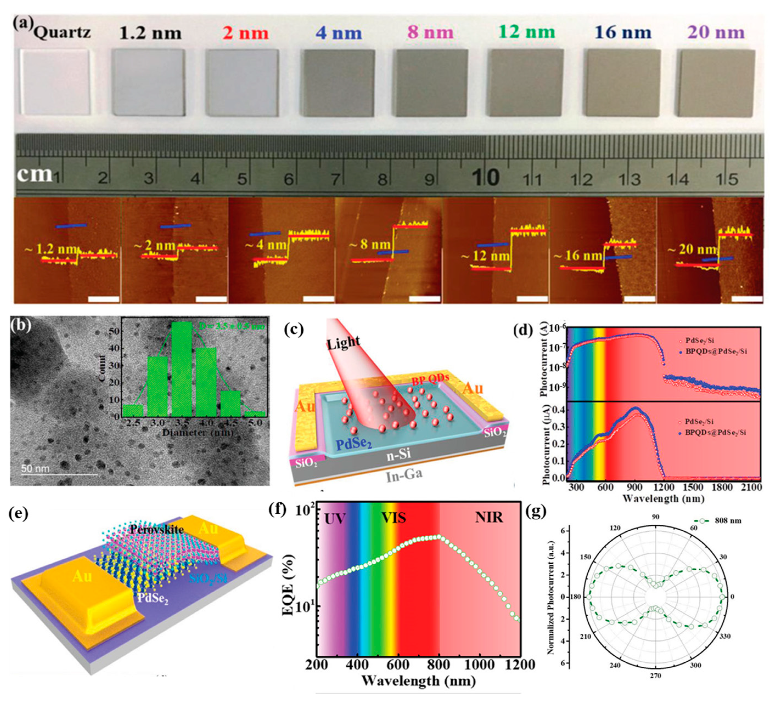
3.4. Layer Dependent Optical Absorption and Bandgap Evolution
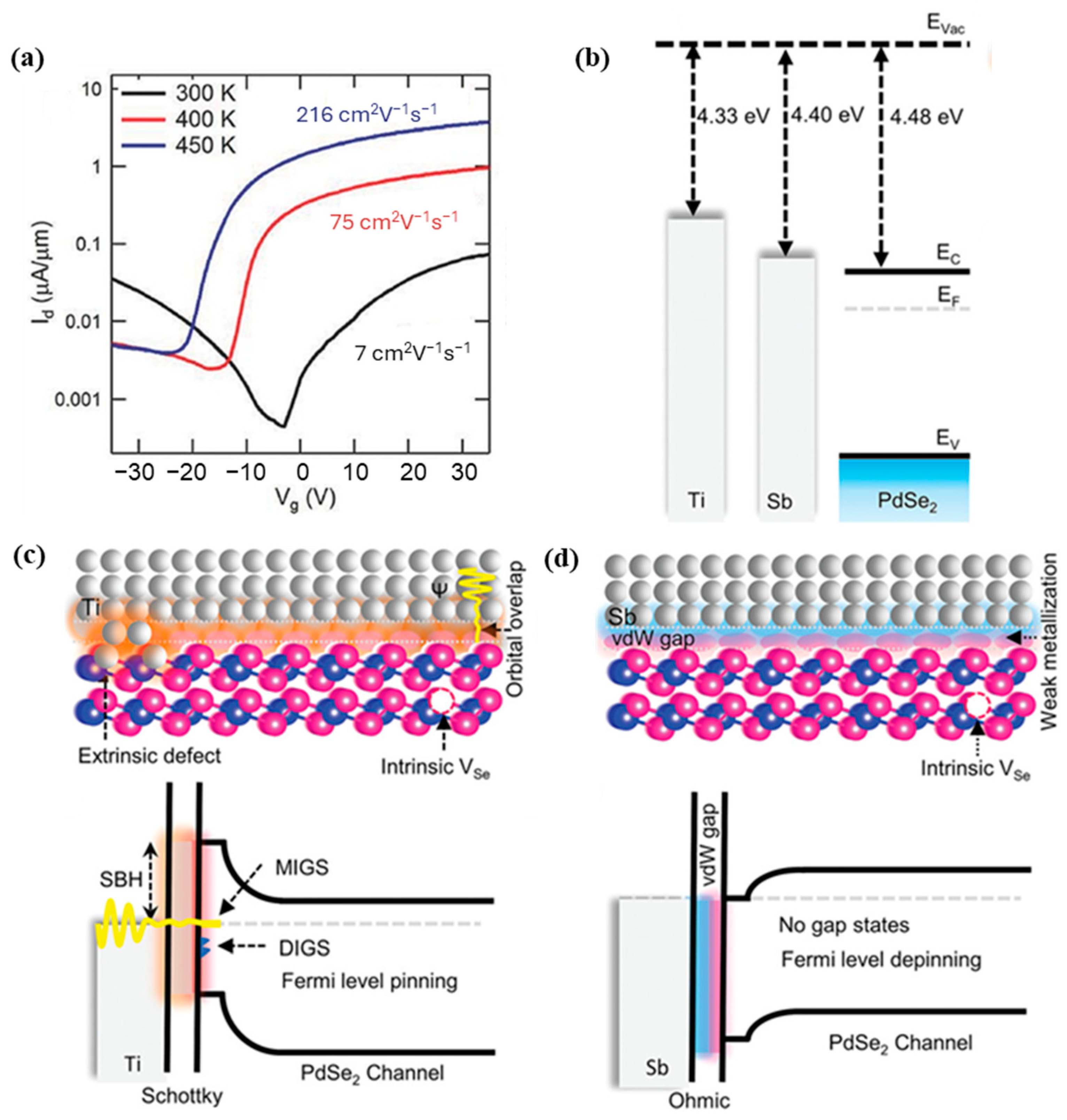
3.5. Carrier Transport Characteristics and Carrier Mobility
4. PdSe2 Photodetectors: Fabrication Methods and Their Performance
4.1. CVD Grown PdSe2 for Photodetectors
4.1.1. Standalone CVD Grown PdSe2 Photodetectors
4.1.2. CVD-PdSe2 Hybrid Heterostructure-Based Photodetectors
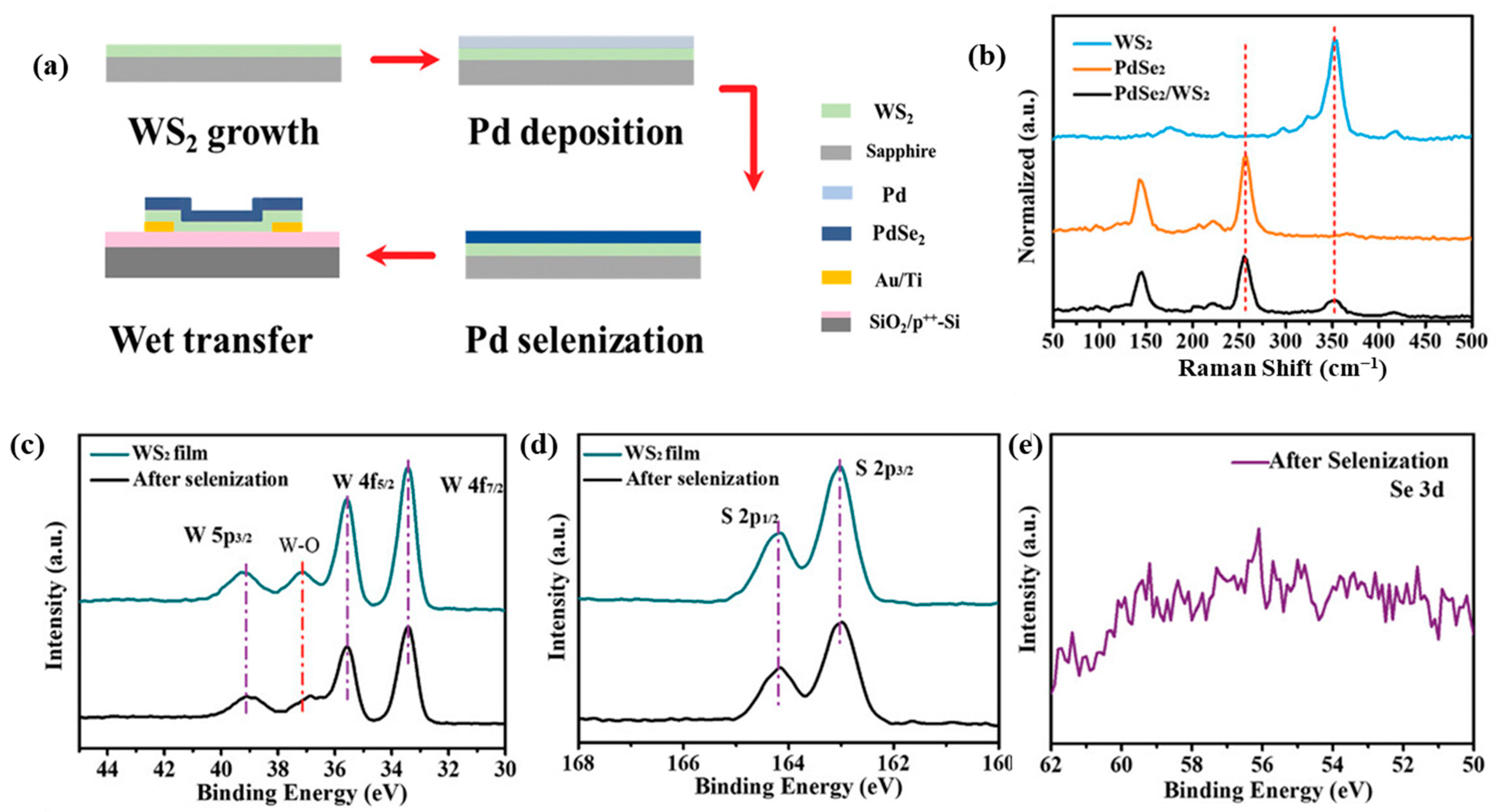
4.1.3. CVD Grown PdSe2-2D Heterostructure-Based Photodetectors
4.2. Mechanically Exfoliated PdSe2 Photodetectors
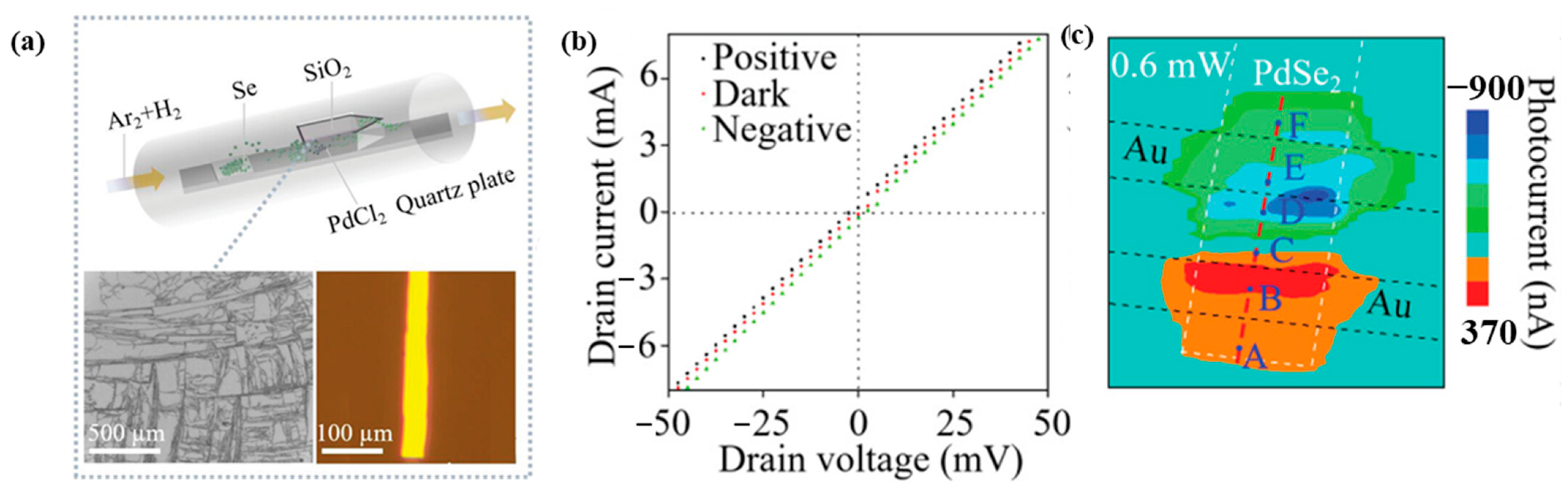
4.2.1. Standalone M.E. PdSe2 Photodetectors
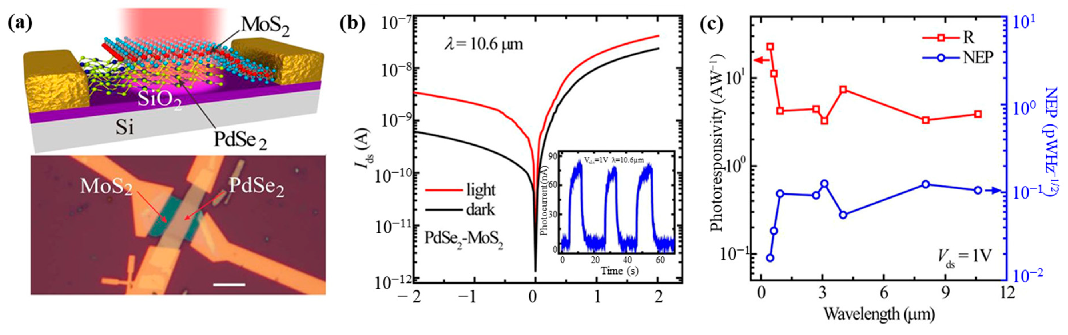
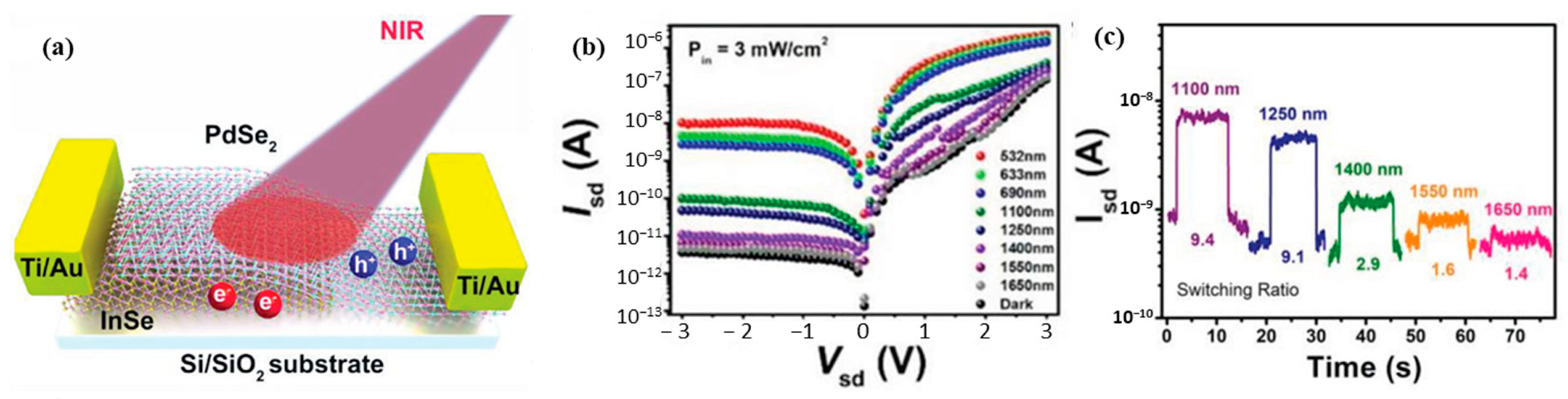
4.2.2. M.E. PdSe2-2D Heterostructure-Based Photodetectors
4.2.3. Graphene-Sandwiched PdSe2-2D Heterostructure-Based Photodetectors
5. Outlook and Perspective
Author Contributions
Funding
Informed Consent Statement
Data Availability Statement
Conflicts of Interest
References
- Novoselov, K.S.; Geim, A.K.; Morozov, S.V.; Jiang, D.; Zhang, Y.; Dubonos, S.V.; Grigorieva, I.V.; Firsov, A.A. Electric Field Effect in Atomically Thin Carbon Films. Science 2004, 306, 666–669. [Google Scholar] [CrossRef] [PubMed]
- Huang, X.; Liu, C.; Zhou, P. 2D Semiconductors for Specific Electronic Applications: From Device to System. NPJ 2D Mater. Appl. 2022, 6, 51. [Google Scholar] [CrossRef]
- Lemme, M.C.; Akinwande, D.; Huyghebaert, C.; Stampfer, C. 2D Materials for Future Heterogeneous Electronics. Nat. Commun. 2022, 13, 1392. [Google Scholar] [CrossRef] [PubMed]
- Illarionov, Y.Y.; Knobloch, T.; Jech, M.; Lanza, M.; Akinwande, D.; Vexler, M.I.; Mueller, T.; Lemme, M.C.; Fiori, G.; Schwierz, F.; et al. Insulators for 2D Nanoelectronics: The Gap to Bridge. Nat. Commun. 2020, 11, 3385. [Google Scholar] [CrossRef] [PubMed]
- Illarionov, Y.Y.; Banshchikov, A.G.; Polyushkin, D.K.; Wachter, S.; Knobloch, T.; Thesberg, M.; Mennel, L.; Paur, M.; Stöger-Pollach, M.; Steiger-Thirsfeld, A.; et al. Ultrathin Calcium Fluoride Insulators for Two-Dimensional Field-Effect Transistors. Nat. Electron. 2019, 2, 230–235. [Google Scholar] [CrossRef]
- Qiu, D.; Gong, C.; Wang, S.S.; Zhang, M.; Yang, C.; Wang, X.; Xiong, J. Recent Advances in 2D Superconductors. Adv. Mat. 2021, 33, 2006124. [Google Scholar] [CrossRef]
- Li, J.; Song, P.; Zhao, J.; Vaklinova, K.; Zhao, X.; Li, Z.; Qiu, Z.; Wang, Z.; Lin, L.; Zhao, M.; et al. Printable Two-Dimensional Superconducting Monolayers. Nat. Mater. 2021, 20, 181–187. [Google Scholar] [CrossRef]
- Kajale, S.N.; Nguyen, T.; Chao, C.A.; Bono, D.C.; Boonkird, A.; Li, M.; Sarkar, D. Current-Induced Switching of a van Der Waals Ferromagnet at Room Temperature. Nat. Commun. 2024, 15, 1485. [Google Scholar] [CrossRef]
- Gibertini, M.; Koperski, M.; Morpurgo, A.F.; Novoselov, K.S. Magnetic 2D Materials and Heterostructures. Nat. Nanotechnol. 2019, 14, 408–419. [Google Scholar] [CrossRef]
- Kang, K.; Xie, S.; Huang, L.; Han, Y.; Huang, P.Y.; Mak, K.F.; Kim, C.J.; Muller, D.; Park, J. High-Mobility Three-Atom-Thick Semiconducting Films with Wafer-Scale Homogeneity. Nature 2015, 520, 656–660. [Google Scholar] [CrossRef]
- Xu, L.; Cai, W.; Jia, Y.; Xing, R.; Han, T.; Zhang, B.; Wang, C. Graphene–Silicon Hybrid MOSFET Integrated Circuits for High-Linearity Analog Amplification. IEEE Elect. Dev. Lett. 2022, 43, 1886–1889. [Google Scholar] [CrossRef]
- Migliato Marega, G.; Zhao, Y.; Avsar, A.; Wang, Z.; Tripathi, M.; Radenovic, A.; Kis, A. Logic-in-Memory Based on an Atomically Thin Semiconductor. Nature 2020, 587, 72–77. [Google Scholar] [CrossRef] [PubMed]
- Dai, T.; Chen, C.; Huang, L.; Jiang, J.; Peng, L.M.; Zhang, Z. Ultrasensitive Magnetic Sensors Enabled by Heterogeneous Integration of Graphene Hall Elements and Silicon Processing Circuits. ACS Nano 2020, 14, 17606–17614. [Google Scholar] [CrossRef] [PubMed]
- Hong, S.K.; Kim, C.S.; Hwang, W.S.; Cho, B.J. Hybrid Integration of Graphene Analog and Silicon Complementary Metal-Oxide-Semiconductor Digital Circuits. ACS Nano 2016, 10, 7142–7146. [Google Scholar] [CrossRef] [PubMed]
- Taffelli, A.; Dirè, S.; Quaranta, A.; Pancheri, L. MoS2 Based Photodetectors: A Review. Sensors 2021, 21, 2758. [Google Scholar] [CrossRef]
- Gupta, S.; Yang, J.H.; Yakobson, B.I. Two-Level Quantum Systems in Two-Dimensional Materials for Single Photon Emission. Nano Lett. 2019, 19, 408–414. [Google Scholar] [CrossRef]
- Samadi, M.; Sarikhani, N.; Zirak, M.; Zhang, H.; Zhang, H.L.; Moshfegh, A.Z. Group 6 Transition Metal Dichalcogenide Nanomaterials: Synthesis, Applications and Future Perspectives. Nanoscale Horiz. 2018, 3, 90–204. [Google Scholar] [CrossRef]
- Lei, W.; Zhang, S.; Heymann, G.; Tang, X.; Wen, J.; Zheng, X.; Hu, G.; Ming, X. A New 2D High-Pressure Phase of PdSe2 with High-Mobility Transport Anisotropy for Photovoltaic Applications. J. Mater. Chem. C 2019, 7, 2096–2105. [Google Scholar] [CrossRef]
- Wang, Z.; Ali, N.; Ngo, T.D.; Shin, H.; Lee, S.; Yoo, W.J. Achieving Ultrahigh Electron Mobility in PdSe2 Field-Effect Transistors via Semimetal Antimony as Contacts. Adv. Funct. Mater. 2023, 33, 2301651. [Google Scholar] [CrossRef]
- Li, G.; Yin, S.; Tan, C.; Chen, L.; Yu, M.; Li, L.; Yan, F. Fast Photothermoelectric Response in CVD-Grown PdSe2 Photodetectors with In-Plane Anisotropy. Adv. Funct. Mater. 2021, 31, 2104787. [Google Scholar] [CrossRef]
- Oyedele, A.D.; Yang, S.; Liang, L.; Puretzky, A.A.; Wang, K.; Zhang, J.; Yu, P.; Pudasaini, P.R.; Ghosh, A.W.; Liu, Z.; et al. PdSe2: Pentagonal Two-Dimensional Layers with High Air Stability for Electronics. J. Am. Chem. Soc. 2017, 139, 14090–14097. [Google Scholar] [CrossRef] [PubMed]
- Dong, Z.; Yu, W.; Zhang, L.; Mu, H.; Xie, L.; Li, J.; Zhang, Y.; Huang, L.; He, X.; Wang, L.; et al. Highly Efficient, Ultrabroad PdSe2 Phototransistors from Visible to Terahertz Driven by Mutiphysical Mechanism. ACS Nano 2021, 15, 20403–20413. [Google Scholar] [CrossRef] [PubMed]
- Zeng, L.H.; Lin, S.H.; Li, Z.J.; Zhang, Z.X.; Zhang, T.F.; Xie, C.; Mak, C.H.; Chai, Y.; Lau, S.P.; Luo, L.B.; et al. Fast, Self-Driven, Air-Stable, and Broadband Photodetector Based on Vertically Aligned PtSe2/GaAs Heterojunction. Adv. Funct. Mater. 2018, 28, 1705970. [Google Scholar] [CrossRef]
- Zhang, H.; Li, H.; Wang, F.; Song, X.; Xu, Z.; Wei, D.; Zhang, J.; Dai, Z.; Ren, Y.; Ye, Y.; et al. PtSe2 Field-Effect Phototransistor with Positive and Negative Photoconductivity. ACS Appl. Electron. Mater. 2022, 4, 5177–5183. [Google Scholar] [CrossRef]
- Rani, A.; Verma, A.; Yadav, B.C. Advancements in Transition Metal Dichalcogenides (TMDCs) for Self-Powered Photodetectors: Challenges, Properties, and Functionalization Strategies. RSC Mater. Adv. 2024, 5, 3535–3562. [Google Scholar] [CrossRef]
- Chen, E.; Xu, W.; Chen, J.; Warner, J.H. 2D Layered Noble Metal Dichalcogenides (Pt, Pd, Se, S) for Electronics and Energy Applications. Mater. Today Adv. 2020, 7, 100076. [Google Scholar] [CrossRef]
- Sun, Y.; Zhang, J.; Ye, S.; Song, J.; Qu, J. Progress Report on Property, Preparation, and Application of Bi2O2Se. Adv. Funct. Mater. 2020, 30, 2004480. [Google Scholar] [CrossRef]
- Yang, Q.; Wang, X.; He, Z.; Chen, Y.; Li, S.; Chen, H.; Wu, S. A Centimeter-Scale Type-II Weyl Semimetal for Flexible and Fast Ultra-Broadband Photodetection from Ultraviolet to Sub-Millimeter Wave Regime. Adv. Sci. 2023, 10, e2205609. [Google Scholar] [CrossRef]
- Guo, Q.; Pospischil, A.; Bhuiyan, M.; Jiang, H.; Tian, H.; Farmer, D.; Deng, B.; Li, C.; Han, S.J.; Wang, H.; et al. Black Phosphorus Mid-Infrared Photodetectors with High Gain. Nano Lett. 2016, 16, 4648–4655. [Google Scholar] [CrossRef]
- Chen, X.; Lu, X.; Deng, B.; Sinai, O.; Shao, Y.; Li, C.; Yuan, S.; Tran, V.; Watanabe, K.; Taniguchi, T.; et al. Widely Tunable Black Phosphorus Mid-Infrared Photodetector. Nat. Commun. 2017, 8, 1672. [Google Scholar] [CrossRef]
- Lee, C.H.; Lee, G.H.; Van Der Zande, A.M.; Chen, W.; Li, Y.; Han, M.; Cui, X.; Arefe, G.; Nuckolls, C.; Heinz, T.F.; et al. Atomically Thin p-n Junctions with van Der Waals Heterointerfaces. Nat. Nanotechnol. 2014, 9, 676–681. [Google Scholar] [CrossRef] [PubMed]
- Liu, X.; Sun, G.; Chen, P.; Liu, J.; Zhang, Z.; Li, J.; Ma, H.; Zhao, B.; Wu, R.; Dang, W.; et al. High-Performance Asymmetric Electrodes Photodiode Based on Sb/WSe2 Heterostructure. Nano Res. 2019, 12, 339–344. [Google Scholar] [CrossRef]
- Lv, Q.; Yan, F.; Wei, X.; Wang, K. High-Performance, Self-Driven Photodetector Based on Graphene Sandwiched GaSe/WS2 Heterojunction. Adv. Opt. Mater. 2018, 6, 1700490. [Google Scholar] [CrossRef]
- Jia, S.; Jin, Z.; Zhang, J.; Yuan, J.; Chen, W.; Feng, W.; Hu, P.; Ajayan, P.M.; Lou, J. Lateral Monolayer MoSe2–WSe2 p–n Heterojunctions with Giant Built-In Potentials. Small 2020, 16, 2002263. [Google Scholar] [CrossRef]
- Choi, M.S.; Qu, D.; Lee, D.; Liu, X.; Watanabe, K.; Taniguchi, T.; Yoo, W.J. Lateral MoS2 p-n Junction Formed by Chemical Doping for Use in High-Performance Optoelectronics. ACS Nano 2014, 8, 9332–9340. [Google Scholar] [CrossRef]
- Kim, J.K.; Cho, K.; Jang, J.; Baek, K.Y.; Kim, J.; Seo, J.; Song, M.; Shin, J.; Kim, J.; Parkin, S.S.P.; et al. Molecular Dopant-Dependent Charge Transport in Surface-Charge-Transfer-Doped Tungsten Diselenide Field Effect Transistors. Adv. Mater. 2021, 33, 2101598. [Google Scholar] [CrossRef]
- Wei, X.; Yan, F.; Lv, Q.; Zhu, W.; Hu, C.; Patanè, A.; Wang, K. Enhanced Photoresponse in MoTe2 Photodetectors with Asymmetric Graphene Contacts. Adv. Opt. Mater. 2019, 7, 1900190. [Google Scholar] [CrossRef]
- Dai, M.; Chen, H.; Wang, F.; Long, M.; Shang, H.; Hu, Y.; Li, W.; Ge, C.; Zhang, J.; Zhai, T.; et al. Ultrafast and Sensitive Self-Powered Photodetector Featuring Self-Limited Depletion Region and Fully Depleted Channel with van Der Waals Contacts. ACS Nano 2020, 14, 9098–9106. [Google Scholar] [CrossRef]
- Qi, Z.; Yang, T.; Li, D.; Li, H.; Wang, X.; Zhang, X.; Li, F.; Zheng, W.; Fan, P.; Zhuang, X.; et al. High-Responsivity Two-Dimensional p-PbI2/n-WS2 Vertical Heterostructure Photodetectors Enhanced by Photogating Effect. Mater. Horiz. 2019, 6, 1474–1480. [Google Scholar] [CrossRef]
- Quan, S.; Li, L.; Guo, S.; Zhao, X.; Weller, D.; Wang, X.; Fu, S.; Liu, R.; Hao, Y. SnS2/MoS2 van Der Waals Heterostructure Photodetector with Ultrahigh Responsivity Realized by a Photogating Effect. ACS Appl. Mater. Interfaces 2023, 15, 59592–59599. [Google Scholar] [CrossRef]
- Lei, T.; Tu, H.; Lv, W.; Ma, H.; Wang, J.; Hu, R.; Wang, Q.; Zhang, L.; Fang, B.; Liu, Z.; et al. Ambipolar Photoresponsivity in an Ultrasensitive Photodetector Based on a WSe2/InSe Heterostructure by a Photogating Effect. ACS Appl. Mater. Interfaces 2021, 13, 50213–50219. [Google Scholar] [CrossRef] [PubMed]
- Yang, Y.; Li, J.; Choi, S.; Jeon, S.; Cho, J.H.; Lee, B.H.; Lee, S. High-Responsivity PtSe2 photodetector Enhanced by Photogating Effect. Appl. Phys. Lett. 2021, 118, 013103. [Google Scholar] [CrossRef]
- Jiang, H.; Wei, J.; Sun, F.; Nie, C.; Fu, J.; Shi, H.; Sun, J.; Wei, X.; Qiu, C.W. Enhanced Photogating Effect in Graphene Photodetectors via Potential Fluctuation Engineering. ACS Nano 2022, 16, 4458–4466. [Google Scholar] [CrossRef] [PubMed]
- Zhang, K.; Peng, M.; Yu, A.; Fan, Y.; Zhai, J.; Wang, Z.L. A Substrate-Enhanced MoS2 Photodetector through a Dual-Photogating Effect. Mater. Horiz. 2019, 6, 826–833. [Google Scholar] [CrossRef]
- Viti, L.; Politano, A.; Zhang, K.; Vitiello, M.S. Thermoelectric Terahertz Photodetectors Based on Selenium-Doped Black Phosphorus Flakes. Nanoscale 2019, 11, 1995–2002. [Google Scholar] [CrossRef]
- Viti, L.; Hu, J.; Coquillat, D.; Knap, W.; Tredicucci, A.; Politano, A.; Vitiello, M.S. Black Phosphorus Terahertz Photodetectors. Adv. Mater. 2015, 27, 5567–5572. [Google Scholar] [CrossRef]
- Gu, Y.; Zhang, L.; Cai, H.; Liang, L.; Liu, C.; Hoffman, A.; Yu, Y.; Houston, A.; Puretzky, A.A.; Duscher, G.; et al. Stabilized Synthesis of 2D Verbeekite: Monoclinic PdSe2 Crystals with High Mobility and In-Plane Optical and Electrical Anisotropy. ACS Nano 2022, 16, 13900–13910. [Google Scholar] [CrossRef]
- Chen, X.; Huang, J.; Chen, C.; Chen, M.; Hu, G.; Wang, H.; Dong, N.; Wang, J. Broadband Nonlinear Photoresponse and Ultrafast Carrier Dynamics of 2D PdSe2. Adv. Opt. Mater. 2022, 10, 2101963. [Google Scholar] [CrossRef]
- Zeng, L.H.; Wu, D.; Lin, S.H.; Xie, C.; Yuan, H.Y.; Lu, W.; Lau, S.P.; Chai, Y.; Luo, L.B.; Li, Z.J.; et al. Controlled Synthesis of 2D Palladium Diselenide for Sensitive Photodetector Applications. Adv. Funct. Mater. 2019, 29, 1806878. [Google Scholar] [CrossRef]
- Zhong, J.; Yu, J.; Cao, L.; Zeng, C.; Ding, J.; Cong, C.; Liu, Z.; Liu, Y. High-Performance Polarization-Sensitive Photodetector Based on a Few-Layered PdSe2 Nanosheet. Nano Res. 2020, 13, 1780–1786. [Google Scholar] [CrossRef]
- Wu, D.; Jia, C.; Shi, F.; Zeng, L.; Lin, P.; Dong, L.; Shi, Z.; Tian, Y.; Li, X.; Jie, J. Mixed-Dimensional PdSe2/SiNWA Heterostructure Based Photovoltaic Detectors for Self-Driven, Broadband Photodetection, Infrared Imaging and Humidity Sensing. J. Mater. Chem. A Mater. 2020, 8, 3632–3642. [Google Scholar] [CrossRef]
- Zhong, J.; Wu, B.; Madoune, Y.; Wang, Y.; Liu, Z.; Liu, Y. PdSe2/MoSe2 Vertical Heterojunction for Self-Powered Photodetector with High Performance. Nano Res. 2022, 15, 2489–2496. [Google Scholar] [CrossRef]
- Lu, L.S.; Chen, G.H.; Cheng, H.Y.; Chuu, C.P.; Lu, K.C.; Chen, C.H.; Lu, M.Y.; Chuang, T.H.; Wei, D.H.; Chueh, W.C.; et al. Layer-Dependent and In-Plane Anisotropic Properties of Low-Temperature Synthesized Few-Layer PdSe2 Single Crystals. ACS Nano 2020, 14, 4963–4972. [Google Scholar] [CrossRef] [PubMed]
- Zeng, L.H.; Chen, Q.M.; Zhang, Z.X.; Wu, D.; Yuan, H.; Li, Y.Y.; Qarony, W.; Lau, S.P.; Luo, L.B.; Tsang, Y.H. Multilayered PdSe2/Perovskite Schottky Junction for Fast, Self-Powered, Polarization-Sensitive, Broadband Photodetectors, and Image Sensor Application. Adv. Sci. 2019, 6, 1901134. [Google Scholar] [CrossRef] [PubMed]
- Puretzky, A.A.; Oyedele, A.D.; Xiao, K.; Haglund, A.V.; Sumpter, B.G.; Mandrus, D.; Geohegan, D.B.; Liang, L. Anomalous Interlayer Vibrations in Strongly Coupled Layered PdSe2. 2D Mater. 2018, 5, 035016. [Google Scholar] [CrossRef]
- Wei, M.Y.; Lian, J.; Zhang, Y.; Wang, C.L.; Wang, Y.; Xu, Z. Layer-Dependent Optical and Dielectric Properties of Centimeter-Scale PdSe2 Films Grown by Chemical Vapor Deposition. NPJ 2D Mater. Appl. 2022, 6, 1. [Google Scholar] [CrossRef]
- Zhang, G.; Amani, M.; Chaturvedi, A.; Tan, C.; Bullock, J.; Song, X.; Kim, H.; Lien, D.H.; Scott, M.C.; Zhang, H.; et al. Optical and Electrical Properties of Two-Dimensional Palladium Diselenide. Appl. Phys. Lett. 2019, 114, 253102. [Google Scholar] [CrossRef]
- Nishiyama, W.; Nishimura, T.; Nishioka, M.; Ueno, K.; Iwamoto, S.; Nagashio, K. Is the Bandgap of Bulk PdSe2 Located Truly in the Far-Infrared Region? Determination by Fourier-Transform Photocurrent Spectroscopy. Adv. Photonics Res. 2022, 3, 2200231. [Google Scholar] [CrossRef]
- Nishiyama, W.; Nishimura, T.; Ueno, K.; Taniguchi, T.; Watanabe, K.; Nagashio, K. Quantitative Determination of Contradictory Bandgap Values of Bulk PdSe2 from Electrical Transport Properties. Adv. Funct. Mater. 2022, 32, 2200231. [Google Scholar] [CrossRef]
- Hoffman, A.N.; Gu, Y.; Liang, L.; Fowlkes, J.D.; Xiao, K.; Rack, P.D. Exploring the Air Stability of PdSe2 via Electrical Transport Measurements and Defect Calculations. NPJ 2D Mater. Appl. 2019, 3, 50. [Google Scholar] [CrossRef]
- Chow, W.L.; Yu, P.; Liu, F.; Hong, J.; Wang, X.; Zeng, Q.; Hsu, C.H.; Zhu, C.; Zhou, J.; Wang, X.; et al. High Mobility 2D Palladium Diselenide Field-Effect Transistors with Tunable Ambipolar Characteristics. Adv. Mater. 2017, 29, 1602969. [Google Scholar] [CrossRef]
- Elghazali, M.A.; Naumov, P.G.; Mirhosseini, H.; Süß, V.; Müchler, L.; Schnelle, W.; Felser, C.; Medvedev, S.A. Pressure-Induced Superconductivity up to 13.1 K in the Pyrite Phase of Palladium Diselenide PdSe2. Phys. Rev. B 2017, 96, 060509. [Google Scholar] [CrossRef]
- Oyedele, A.D.; Yang, S.; Feng, T.; Haglund, A.V.; Gu, Y.; Puretzky, A.A.; Briggs, D.; Rouleau, C.M.; Chisholm, M.F.; Unocic, R.R.; et al. Defect-Mediated Phase Transformation in Anisotropic Two-Dimensional PdSe2 Crystals for Seamless Electrical Contacts. J. Am. Chem. Soc. 2019, 141, 8928–8936. [Google Scholar] [CrossRef] [PubMed]
- Alam, T.I.; Hani, S.U.; Ahmed, S.; Tsang, Y.H. All van der Waals Photodetector for Ultralow Dark Current. In Proceedings of the SPIE—The International Society for Optical Engineering, San Francisco, CA, USA, 27 January–1 February 2024; p. 38. [Google Scholar] [CrossRef]
- Zhang, R.; Yang, Z.; Liu, L.; Lin, J.; Wen, S.; Meng, Y.; Yin, Y.; Lan, C.; Li, C.; Liu, Y.; et al. Highly Sensitive Broadband Bolometric Photodetectors Based on 2D PdSe2 Thin Film. Adv. Opt. Mater. 2023, 11, 2301055. [Google Scholar] [CrossRef]
- Wu, D.; Xu, M.; Zeng, L.; Shi, Z.; Tian, Y.; Li, X.J.; Shan, C.X.; Jie, J. In Situ Fabrication of PdSe2/GaN Schottky Junction for Polarization-Sensitive Ultraviolet Photodetection with High Dichroic Ratio. ACS Nano 2022, 16, 5545–5555. [Google Scholar] [CrossRef] [PubMed]
- Gao, H.; Du, C.; Chen, L.; Wang, W.; Li, K. Van Der Waals MoS2/PdSe2 Heterostructures Grown by Chemical Vapor Deposition for Broadband and Polarized Photodetection. Adv. Mater. Interfaces 2022, 9, 2102350. [Google Scholar] [CrossRef]
- Kang, X.; Lan, C.; Li, F.; Wang, W.; Yip, S.P.; Meng, Y.; Wang, F.; Lai, Z.; Liu, C.; Ho, J.C. Van Der Waals PdSe2/WS2 Heterostructures for Robust High-Performance Broadband Photodetection from Visible to Infrared Optical Communication Band. Adv. Opt. Mater. 2021, 9, 2001991. [Google Scholar] [CrossRef]
- Shi, H.; Chen, H.; Wei, Z.; Luo, W.; Ouyang, F. High Performance Photodetector Based on PdSe2/MoS2 heterojunction. J. Phys. Conf. Ser. IOP 2022, 2263, 012025. [Google Scholar] [CrossRef]
- Liang, Q.; Wang, Q.; Zhang, Q.; Wei, J.; Lim, S.X.; Zhu, R.; Hu, J.; Wei, W.; Lee, C.; Sow, C.H.; et al. High-Performance, Room Temperature, Ultra-Broadband Photodetectors Based on Air-Stable PdSe2. Adv. Mater. 2019, 31, e1807609. [Google Scholar] [CrossRef]
- Wu, J.; Ma, H.; Zhong, C.; Wei, M.; Sun, C.; Ye, Y.; Xu, Y.; Tang, B.; Luo, Y.; Sun, B.; et al. Waveguide-Integrated PdSe2 Photodetector over a Broad Infrared Wavelength Range. Nano Lett. 2022, 22, 6816–6824. [Google Scholar] [CrossRef]
- Long, M.; Wang, Y.; Wang, P.; Zhou, X.; Xia, H.; Luo, C.; Huang, S.; Zhang, G.; Yan, H.; Fan, Z.; et al. Palladium Diselenide Long-Wavelength Infrared Photodetector with High Sensitivity and Stability. ACS Nano 2019, 13, 2511–2519. [Google Scholar] [CrossRef] [PubMed]
- Ahmad, W.; Liu, J.; Jiang, J.; Hao, Q.; Wu, D.; Ke, Y.; Gan, H.; Laxmi, V.; Ouyang, Z.; Ouyang, F.; et al. Strong Interlayer Transition in Few-Layer InSe/PdSe2 van Der Waals Heterostructure for Near-Infrared Photodetection. Adv. Funct. Mater. 2021, 31, 2104143. [Google Scholar] [CrossRef]
- Afzal, A.M.; Dastgeer, G.; Iqbal, M.Z.; Gautam, P.; Faisal, M.M. High-Performance p-BP/n-PdSe2 Near-Infrared Photodiodes with a Fast and Gate-Tunable Photoresponse. ACS Appl. Mater. Interf. 2020, 12, 19625–19634. [Google Scholar] [CrossRef] [PubMed]
- Chen, T.; Xiao, L.; Liu, Y.; Wang, J.; Wang, X.; Wang, X.; Yan, S.; Shi, Y. Gate-Tunable Photovoltaic Efficiency in Graphene-Sandwiched PdSe2 Photodetectors with Restrained Carrier Recombination. Adv. Opt. Mater. 2023, 11, 2300167. [Google Scholar] [CrossRef]
- Walmsley, T.S.; Andrews, K.; Wang, T.; Haglund, A.; Rijal, U.; Bowman, A.; Mandrus, D.; Zhou, Z.; Xu, Y.Q. Near-Infrared Optical Transitions in PdSe2 Phototransistors. Nanoscale 2019, 11, 14410–14416. [Google Scholar] [CrossRef]
- Wen, S.; Zhang, R.; Yang, Z.; Zhou, S.; Gong, Y.; Fan, H.; Yin, Y.; Lan, C.; Li, C.; Liu, Y. Gate-Tunable Responsivity of PdSe2 Nanosheet-Based Bolometric Photodetectors for Mid-Infrared Light Detection. ACS Appl. Nano Mater. 2023, 6, 16970–16976. [Google Scholar] [CrossRef]
- Liang, F.X.; Zhao, X.Y.; Jiang, J.J.; Hu, J.G.; Xie, W.Q.; Lv, J.; Zhang, Z.X.; Wu, D.; Luo, L.B. Light Confinement Effect Induced Highly Sensitive, Self-Driven Near-Infrared Photodetector and Image Sensor Based on Multilayer PdSe2/Pyramid Si Heterojunction. Small 2019, 15, e1903831. [Google Scholar] [CrossRef]
- Luo, L.B.; Wang, D.; Xie, C.; Hu, J.G.; Zhao, X.Y.; Liang, F.X. PdSe2 Multilayer on Germanium Nanocones Array with Light Trapping Effect for Sensitive Infrared Photodetector and Image Sensing Application. Adv. Funct. Mater. 2019, 29, 1900849. [Google Scholar] [CrossRef]


| FoM Parameter | Definition | Expression | Unit |
|---|---|---|---|
| Responsivity | Ratio of Photocurrent (Iphoto) to the incident light power (Pin). | A/W | |
| External Quantum Efficiency | Ratio of number of photogenerated electrons per unit time to the number of incident photons. Also referred to as the product of charge transfer efficiency and light absorption efficiency. [h is the Planck constant, e is the electronic charge, c is the light speed, and λ is the incident wavelength of light source] | - | |
| Dark Current | Current persistent in the photodetector under dark/no light conditions. | A | |
| Gain | Ratio of number of photogenerated e-h pairs collected by the contacts to the number of photoexcited e-h pairs. [µ is the carrier mobility, Vbias is the applied bias, L is the channel length, τlife is the carrier lifetime, and τtransit is the carrier transit time.] | - | |
| Linear Dynamic Range | It is the range of illumination log power density for which the log range of photocurrent shows linearity, before reaching saturation. | dB | |
| Response time | The rise (decay) time is defined as the time for the photocurrent to reach 10–90% (90–10%), after introduction (removal) of incident photon flux. | s | |
| 3dB bandwidth @ Relative balance | The cut-off frequency f3dB, of modulated incident light when the responsivity of the photodetector decreases by 3dB (0.707 of the stable value). At a much lower frequency, the responsivity is independent of the light modulation frequency. [Imax and Imin are the maximum and minimum photocurrent] | Hz | |
| Noise Current | AHz−1/2 | ||
| Noise Equivalent Power | The minimum light power that is detectable by a detector is defined as the light power when the signal-to-noise ratio (SNR) is 1. [A is the effective device area.] | WHz−1/2 | |
| Measured Specific Detectivity | It is a measure of a detector’s ability to resolve the weakest of the incident light signal | cmHz1/2W−1 (Jones) | |
| Calculated Specific Detectivity | Specific detectivity is calculated, assuming that the major contribution of noise is from dark current shot noise. | cmHz1/2W−1 (Jones) |
| Channel Material [Fabrication Method] {Structure} | Bandwidth [Operation] | Mobility (cm2V−1s−1) Electron {Hole} | Contact Types | On/Off Ratio | Response Time (ms) Rise/Fall [Wavelength] | Responsivity (AW−1) [Wavelength] | Detectivity (Jones) [Wavelength] | Ref |
|---|---|---|---|---|---|---|---|---|
| PdSe2 [M.E.-Flake] {Waveguide} | 1260 nm–1565 nm [P.C.] | 216 | Ti/Au (B.C.) | - | - | 1.758 [1550 nm] | - | [71] |
| PdSe2 [M.E.-Flake] {FET} | 405 nm–1.249 mm [P.C./P.V.] | 121 | Ni/Au (T.C.) Cr/Au (T.C.) | - | 7.5 × 10⁻³ | 5 × 10⁻³ [1.249 mm] | 1.84 × 10¹² [1850 nm] | [22] |
| PdSe2 [M.E.-Flake] {FET} | 532 nm–4.05 µm [P.C./P.G.] | 4 | Cr/Au (T.C.) | - | - | 708 [1064 nm] | 1.31 × 10⁹ [1064 nm] | [70] |
| PdSe2 [M.E.-Flake] {FET} | 1064 nm [P.T.E.] | 92 | Ti/Au (T.C.) | 104 | 0.156/0.163 | - | - | [76] |
| PdSe2 [M.E.-Flake] {FET} | 9.3 µm [P.B.] | - | Cr/Au (T.C.) | - | 210/230 | 245 × 10−3 [9.3 µm] | - | [77] |
| PdSe2-MoS2 [M.E.-Flake] {L.H. FET} | 450 nm–10.6 µm [P.C./P.G.] | 138.9 {57.7} | Pd/Au (T.C.) | 103 | 74.5/91.3 [10.6 µm] | 42.1 [10.6 µm] | 1.10 × 10⁹ [10.6 µm] | [72] |
| PdSe2-InSe [M.E.-Flake] {L.H. FET} | 532 nm–1650 nm [P.C.] | - | Ti/Au (T.C.) | 3.8 × 10⁴ | 53/72 [532 nm] | 161 [1250 nm] | 1 × 10¹⁰ [1650 nm] | [73] |
| BP-PdSe2 [M.E.-Flake] {L.H. FET} | 532 nm–1310 nm [P.V./P.G.] | - | Cr/Au and Sc/Au (T.C.) | 9.5 × 10⁵ | 1.6/4.7 [1310 nm] | 9.6 × 10⁵ [532 nm] | 5.8 × 10¹³ [532 nm] | [74] |
| Gr-PdSe2-MoS2-Gr [M.E.-Flake] {V.H.} | 650 nm [P.V.] | - | Au-vdW (T.C.) | 107 | 0.129/0.146 | 0.173 [650 nm] | 6.7 × 10¹¹ [650 nm] | [75] |
| Gr-PdSe2-MoSe2-Gr [M.E.-Flake] {V.H.} | 405 nm–1060 nm [P.V.] | - | Cr/Au (B.C.) | 5.6 × 10³ | 41.7 × 10⁻³/ 62.5 × 10⁻³ | 0.651 [532 nm] | 5.29 × 10¹¹ [532 nm] | [52] |
| PdSe2 [CVD-Flake] {FET} | 405 nm–940 nm [P.T.E.] | - | Au-vdW (T.C.) | 2.8 × 10² | 4 × 10⁻³/ 14 × 10−3 | 1.4 × 10⁻³ | 2.55 × 10⁷ | [20] |
| PdSe2 [CVD-Flake] {FET} | 365 nm–2200 nm [P.B.] | - | In/Au (T.C.) | - | 1000/1200 | 37.6 × 10⁻³ [1550nm] | - | [65] |
| PdSe2-MoS2 [CVD-M.E. Flake] {V.H.} | 405 nm–1000 nm [P.C.] | - | Au (T.C.) | 102 | 378/708 [830 nm] | 6.9 [830 nm] | 6.3 × 10¹⁰ [830 nm] | [67] |
| PdSe2-WS2 [CVD] {V.H. FET} | 532 nm–1550 nm [P.C./P.G.] | 3.5 × 10⁻² {2.7 × 10⁻⁴} | Ti/Au (B.C.) | - | 49/90 [635 nm] | 0.019 × 10⁻³ | - | [68] |
| BPQD-PdSe2-Si [CVD-Spin coating] {0D-2D-3D Hybrid V.H.} | 200 nm–3044 nm [P.V.] | - | Au (T.C.) In-Ga (B.C.) | 105 | 38 × 10−3/ 44 × 10−3 | 300.2 × 10⁻³ | 1.18 × 10¹³ | [49] |
| PdSe2-GaN [CVD] {2D-3D Hybrid L.H.} | 200 nm–370 nm [P.V.] | - | Au and Ni/Au (T.C.) | 1.4 × 10³ | 28.5 × 10⁻³/ 122.6 × 10⁻³ | 249.9 × 10⁻³ [360 nm] | 7.9 × 10¹² | [66] |
| PdSe2-Cs-doped FAPbI3 [CVD-Spin coating] {2D-Perovskite Hybrid L.H.} | 200 nm–1550 nm [P.V.] | {4.75} | Au (T.C.) | 104 | 3.5 × 10⁻³/ 4 × 10⁻³ | 313 × 10−3 | 1013 | [54] |
| PdSe2-SiNW [CVD] {2D-3D Hybrid V.H.} | 200 nm–4.6 µm [P.V.] | - | Au (T.C.) In-Ga (B.C.) | 102 | 25.1 × 10⁻³/ 34 × 10−3 | 726 × 10−3 | 3.19 × 10¹⁴ | [51] |
| PdSe2-Si Pyramid [CVD] {2D-3D Hybrid V.H.} | 980 nm–1650 nm [P.V.] | - | Au (T.C.) In-Ga (B.C.) | 1.6 × 10⁵ | N.A. | 456 × 10−3 [980 nm] | 9.97 × 10¹³ [980 nm] | [78] |
| PdSe2-GeNCs CVD 2D-3D Hybrid V.H. | 980 nm–1650 nm [P.V.] | - | Gr-Ag (T.C.) In-Ga (B.C.) | 5 | 25.4 × 10⁻³/ 38.5 × 10⁻³ [1550 nm] | 530.2 × 10⁻³ [1550 nm] | 1.45 × 10¹¹ [1550 nm] | [79] |
Disclaimer/Publisher’s Note: The statements, opinions and data contained in all publications are solely those of the individual author(s) and contributor(s) and not of MDPI and/or the editor(s). MDPI and/or the editor(s) disclaim responsibility for any injury to people or property resulting from any ideas, methods, instructions or products referred to in the content. |
© 2024 by the authors. Licensee MDPI, Basel, Switzerland. This article is an open access article distributed under the terms and conditions of the Creative Commons Attribution (CC BY) license (https://creativecommons.org/licenses/by/4.0/).
Share and Cite
Alam, T.I.; Liu, K.; Hani, S.U.; Ahmed, S.; Tsang, Y.H. Advances in Group-10 Transition Metal Dichalcogenide PdSe2-Based Photodetectors: Outlook and Perspectives. Sensors 2024, 24, 6127. https://doi.org/10.3390/s24186127
Alam TI, Liu K, Hani SU, Ahmed S, Tsang YH. Advances in Group-10 Transition Metal Dichalcogenide PdSe2-Based Photodetectors: Outlook and Perspectives. Sensors. 2024; 24(18):6127. https://doi.org/10.3390/s24186127
Chicago/Turabian StyleAlam, Tawsif Ibne, Kunxuan Liu, Sumaiya Umme Hani, Safayet Ahmed, and Yuen Hong Tsang. 2024. "Advances in Group-10 Transition Metal Dichalcogenide PdSe2-Based Photodetectors: Outlook and Perspectives" Sensors 24, no. 18: 6127. https://doi.org/10.3390/s24186127
APA StyleAlam, T. I., Liu, K., Hani, S. U., Ahmed, S., & Tsang, Y. H. (2024). Advances in Group-10 Transition Metal Dichalcogenide PdSe2-Based Photodetectors: Outlook and Perspectives. Sensors, 24(18), 6127. https://doi.org/10.3390/s24186127