
Design and Manufacture of Multifunctional 3-D Smart Skins with Embedded Sensor Networks for Robotic Applications

 ,
,  , and
, and 
Abstract
1. Introduction
1.1. Background
1.2. Motivation
1.3. Problem Statement
2. Related Work
3. Proposed Method
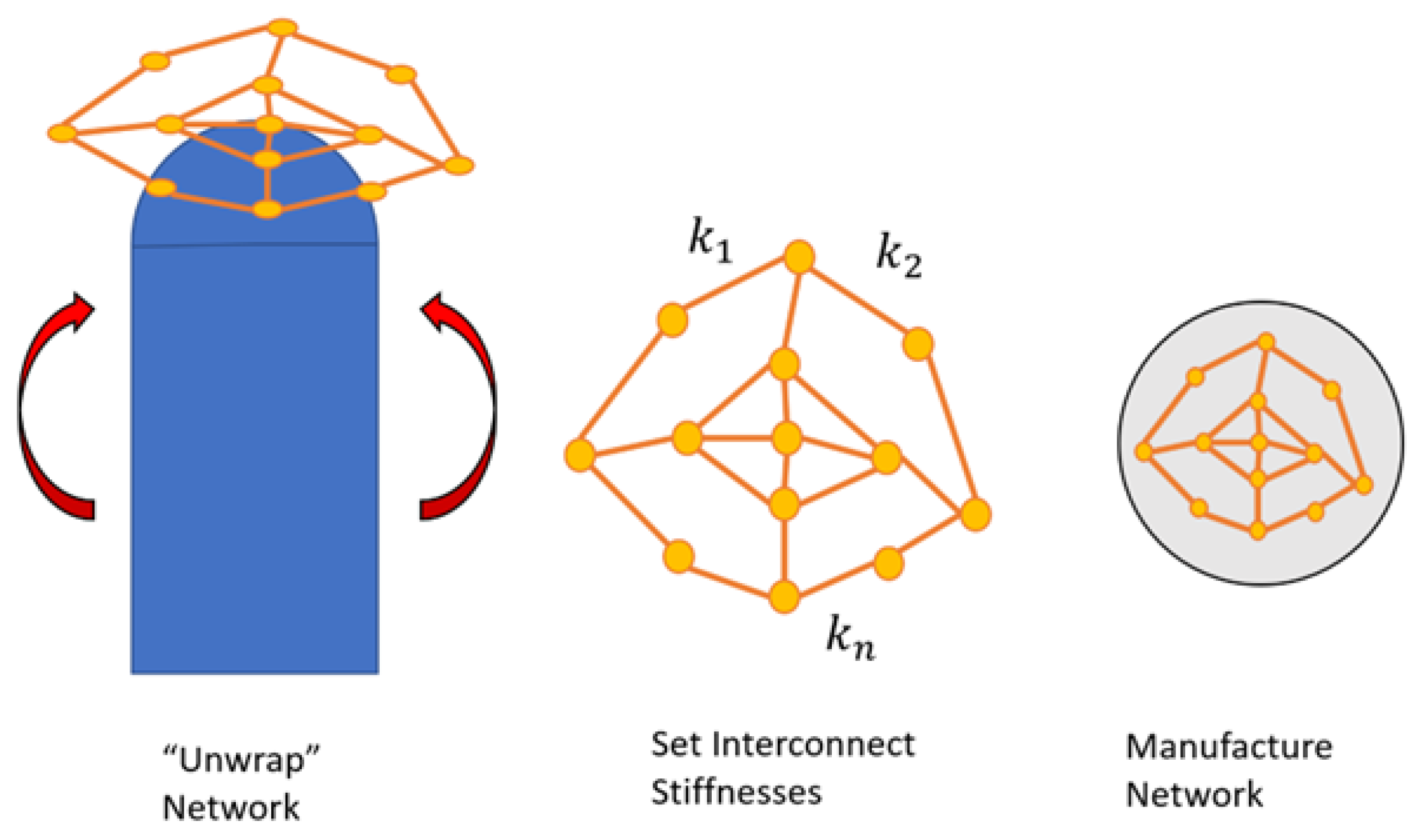
4. Method of Approach
4.1. Overview
4.2. Theory and Design
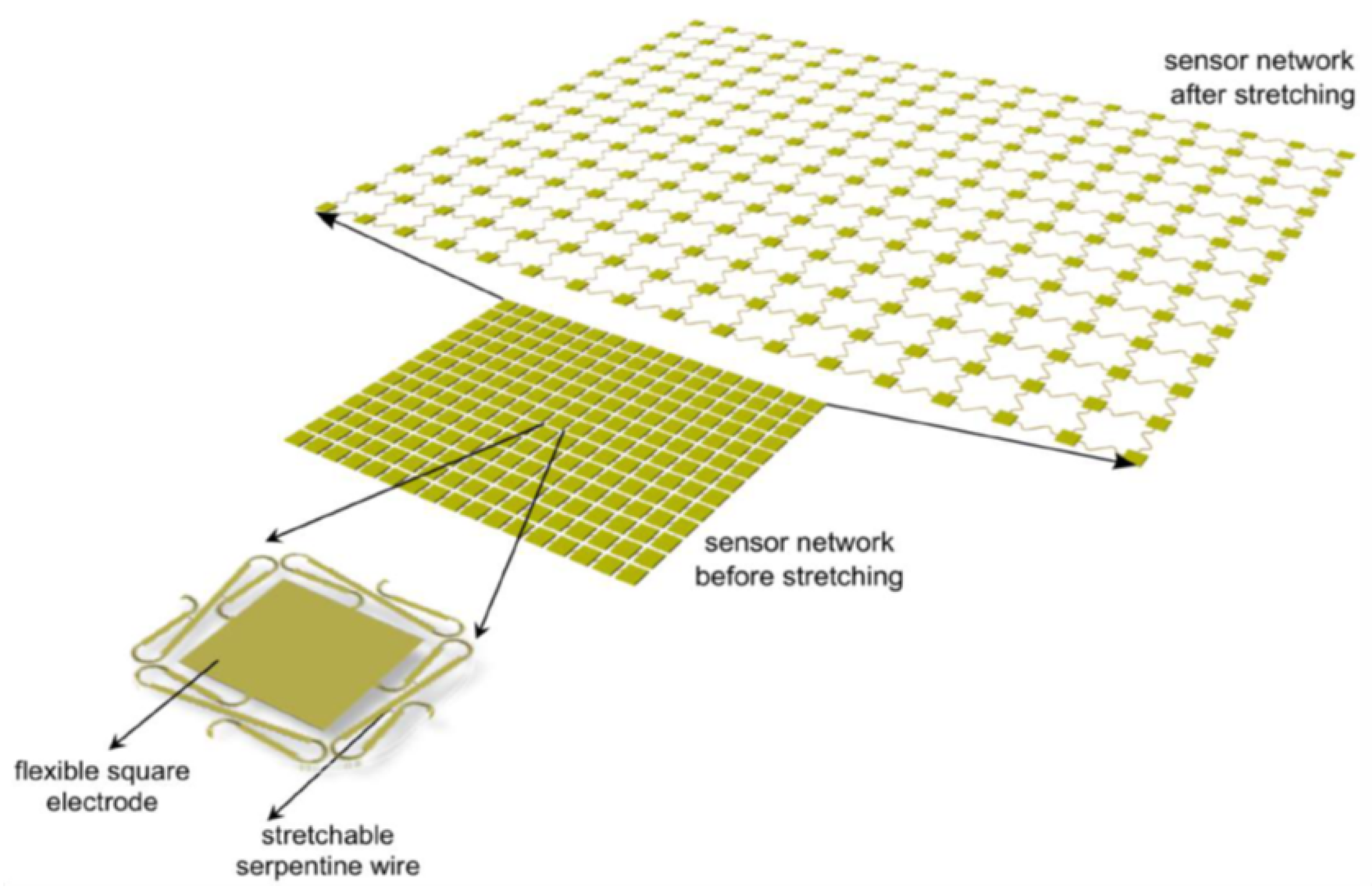
- The determination of target sensor locations.
- The back-design of wire interconnects to satisfy these target locations.
- The manufacture of the sensor network in the SNF.
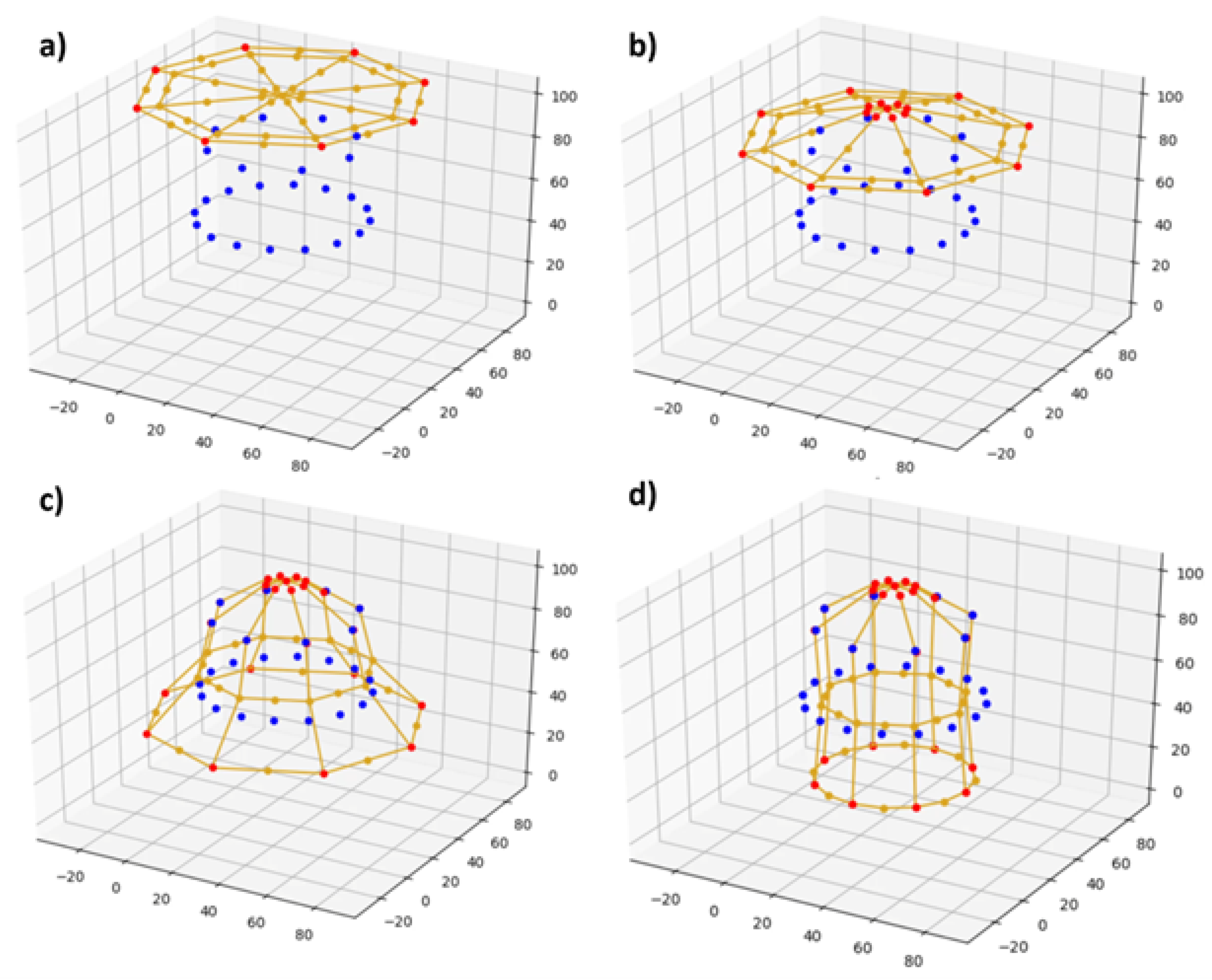
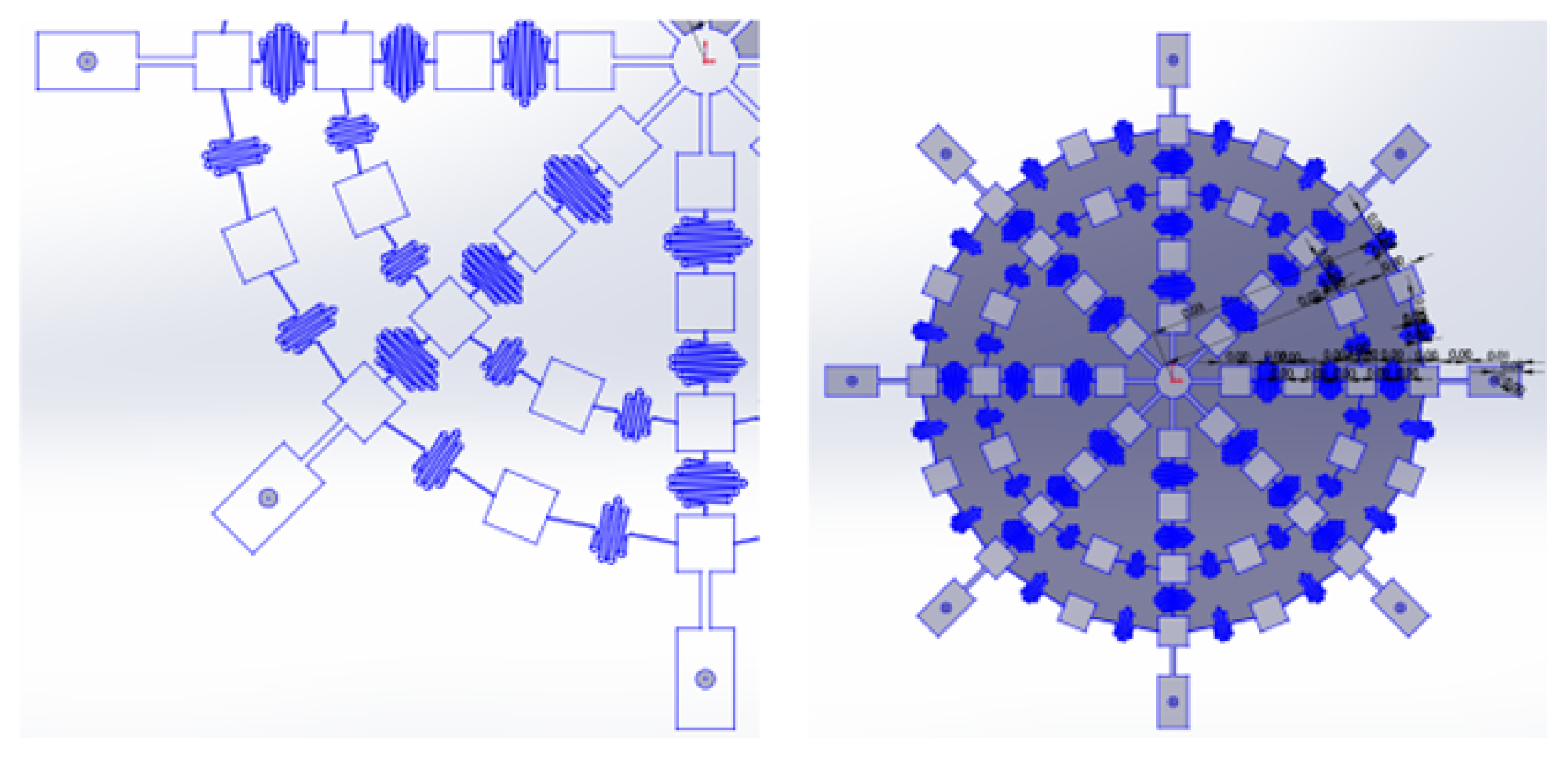
4.2.1. Physics-Based Simulation
- The edge nodes are moved some small distances along their predetermined paths, and their positions are updated in the simulation.
- The positions of the interior nodes are calculated. This is accomplished by performing an L-BFGS-B optimization.
- Nodes are checked for collision with the target geometry. If a node is found to be in contact with the target geometry, it is fixed at the point of contact for the remainder of the simulation.
- Steps 1–3 are repeated until the edge nodes have reached the ends of their predetermined paths.
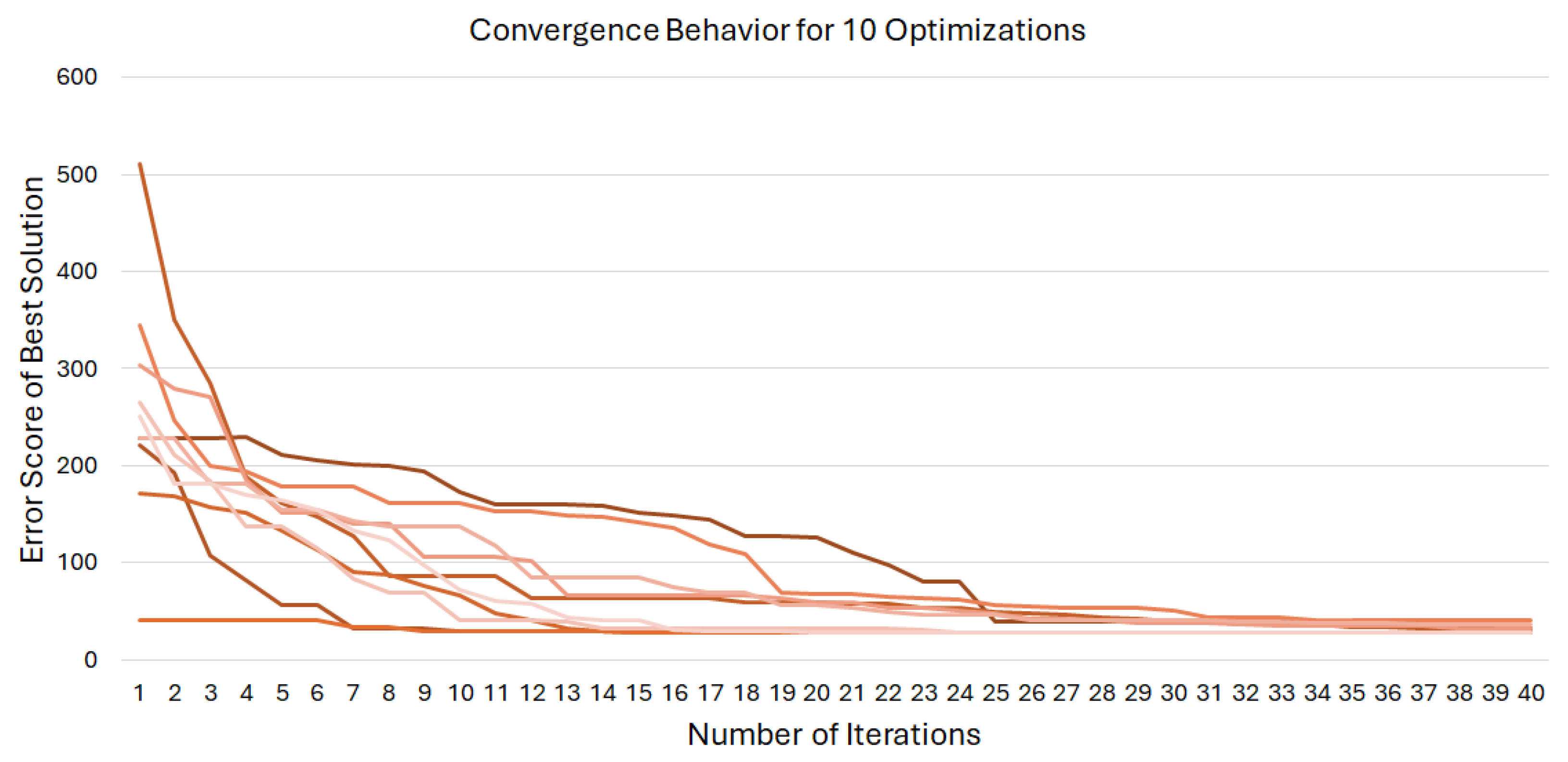
4.2.2. Optimization
- A population of “guesses” in the parameter space is generated. In these initial guesses, the values of the spring stiffness are generated randomly. These ”guesses” form the set of particles, and their parameter values are their “positions” in the parameter space.
- Each particle is evaluated for fitness by running the aforementioned physical simulation corresponding to its parameters. The simulation is scored based on the loss function.
- The resulting particles are sorted by their fitness score after they have all been evaluated.
- The positions of the fittest particles in the simulation history are averaged to generate a “center of gravity”; that is, a point in the parameter space that attracts the particles.
- The particles are given “velocities” in the parameter space with terms corresponding to a decaying “inertial” term proportional to the current velocity of the particle and a term proportional to the distance from the center of gravity of the particle.
- The positions of the particles are updated based on the given velocities.
- This loop from the evaluation to position update repeats for several iterations until the particles swarm around a suitable optimum.
- The coefficients of the velocity terms;
- The size of the weighted average used to determine the center of gravity;
- The numbers of iterations and particles.
- k is the iteration number of the routine;
- v is the velocity of the particle;
- x is the position of the particle;
- is the coefficient corresponding to the inertial term;
- is the coefficient corresponding to the center-of-gravity term;
- n is the total number of iterations;
- R is a random adjustment to the velocity value.
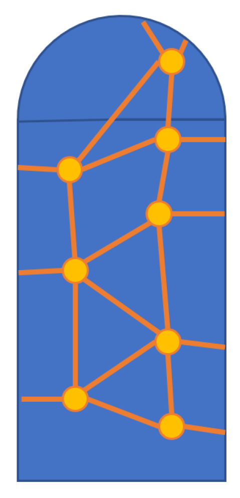
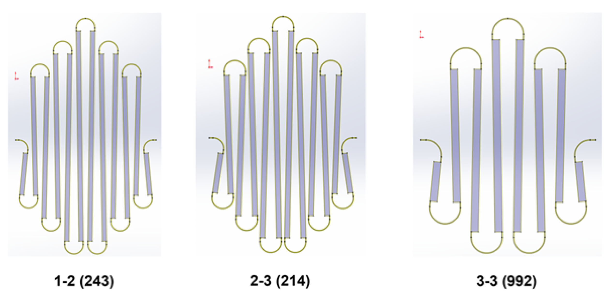
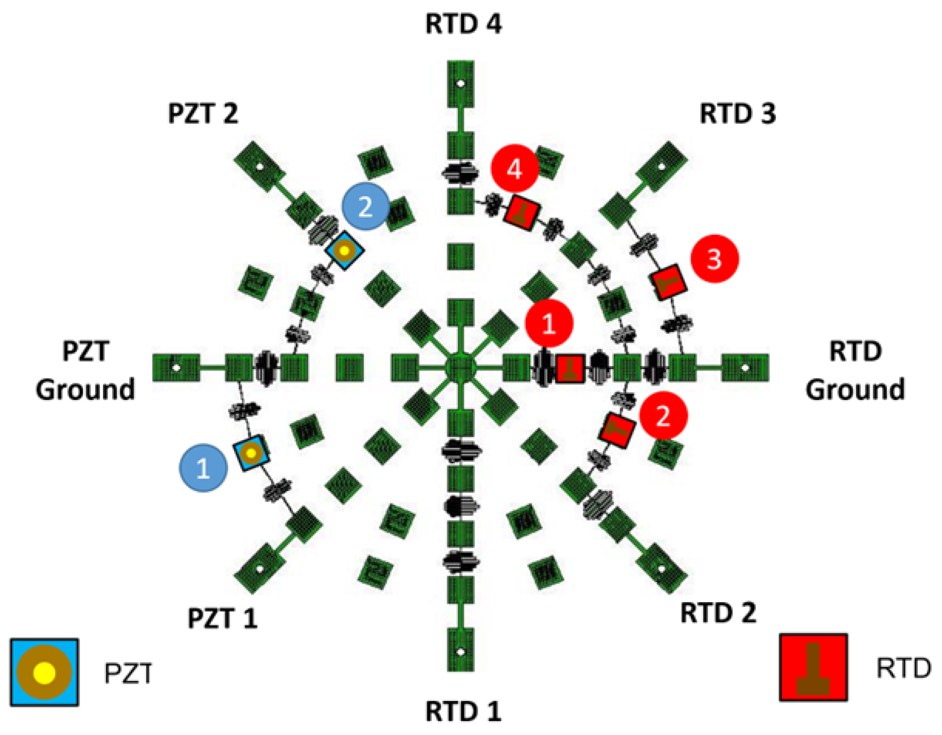
4.3. Design Results
5. Experimental Procedure
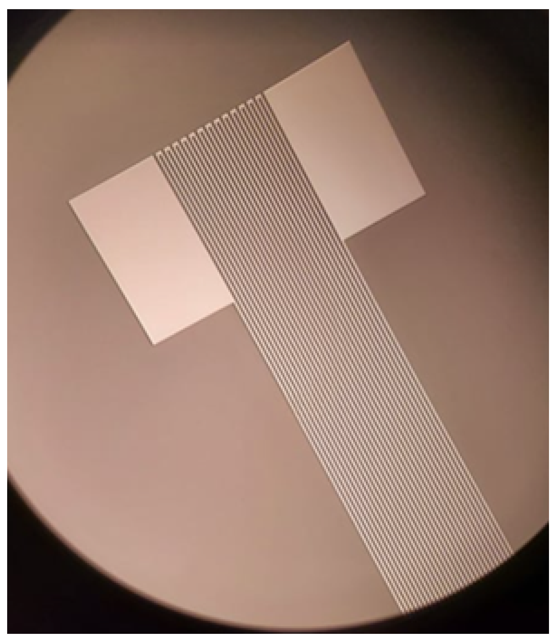
5.1. SSN Microfabrication
- A silicon dioxide etch stop layer was created using low-pressure chemical vapor deposition.
- A germanium sacrificial layer was deposited via e-beam evaporation.
- A polyimide layer, which serves as the bottom encapsulation layer of the finished SSN, was spin-coated on the wafer.
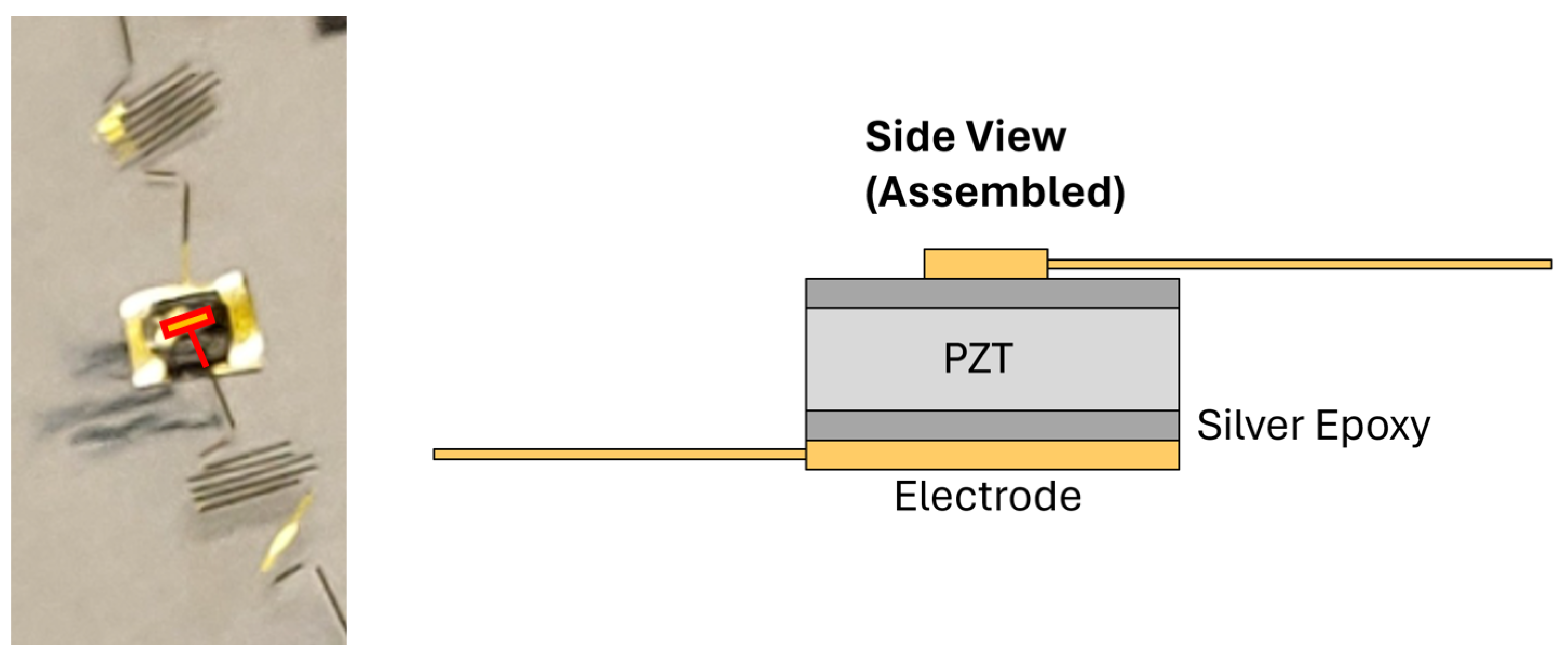
- Titanium (for the RTD-sensing elements) and gold (for the signal layer and PZT electrodes) were deposited over a patterned photoresist mask.
- The top encapsulating layer of polyimide was spin-coated onto the wafer.
- An aluminum etch mask was patterned, which defines the geometry of the finished network.
- The device was plasma-etched and then wet-etched to release it from the wafer, producing the completed SSN.
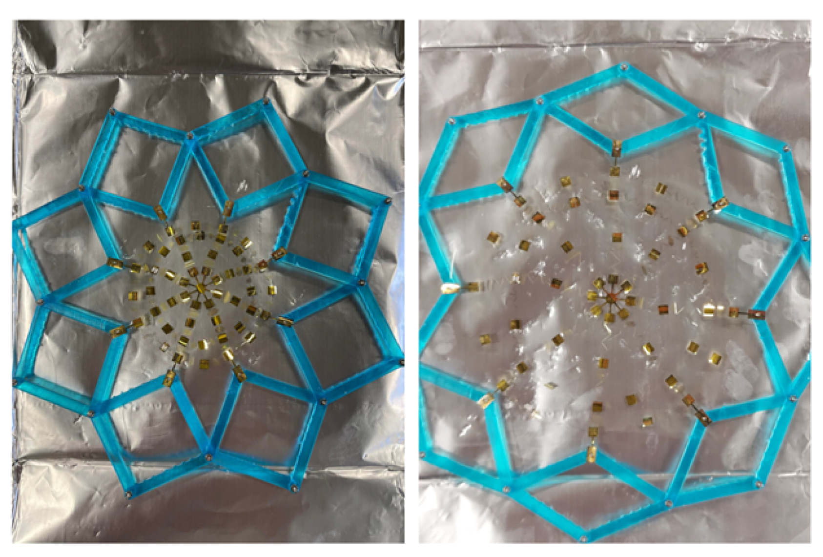
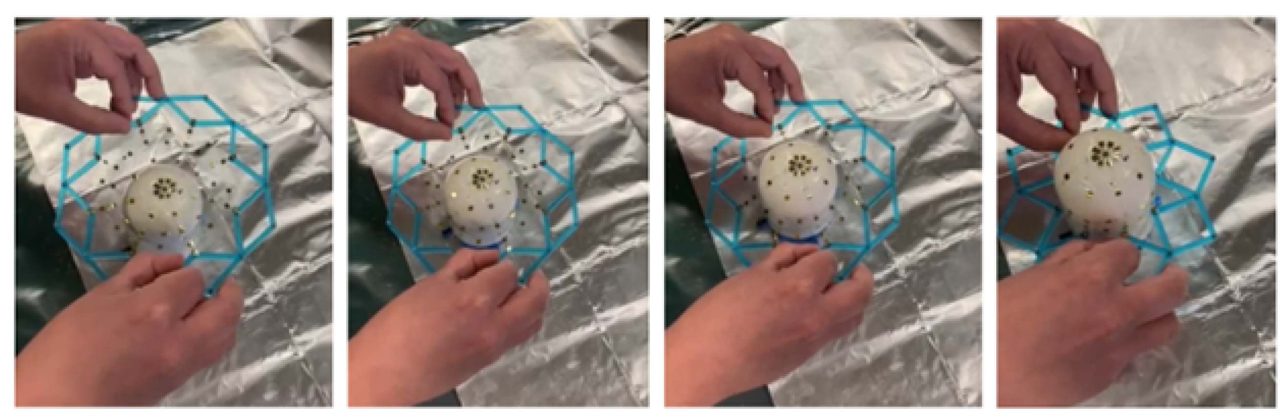
5.2. Polar Stretch Tool
- The edge nodes are radially symmetric and must remain equidistant from one another.
- The edge nodes will always lie on a circle with the same center (i.e., will always trace out similar geometries).
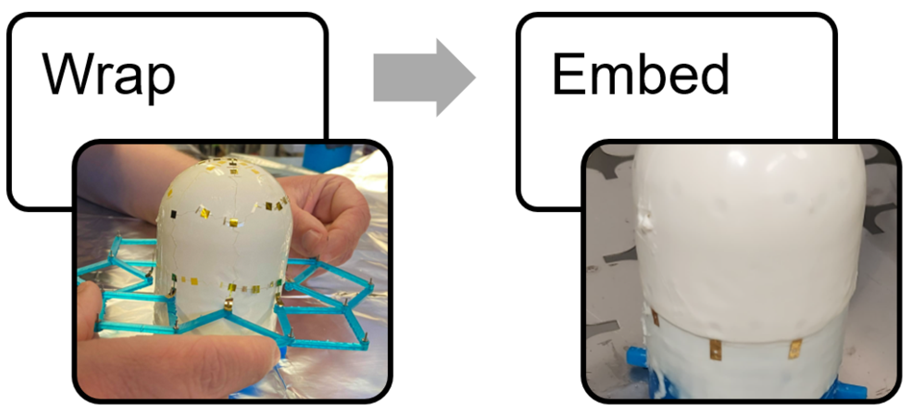
- The network is expanded from its design footprint to its deployment footprint.
- The network is positioned such that the center node comes into contact with the pole of the hemispherical portion of the prepared form.
- The tool is swept straight downward until it is in line with the base of the form.
- The tool is contracted to bring the network in contact with the sidewall.
5.3. Embedding the SSN in a Compliant Skin
5.4. Survey of Materials
- Super-X (brush-applied adhesive);
- Silicone (two-part mold-making silicone system);
- Brush-applied silicone (one part silicone system);
- Aerosol adhesives;
- Latex rubber (dipping-applied coagulant latex system).
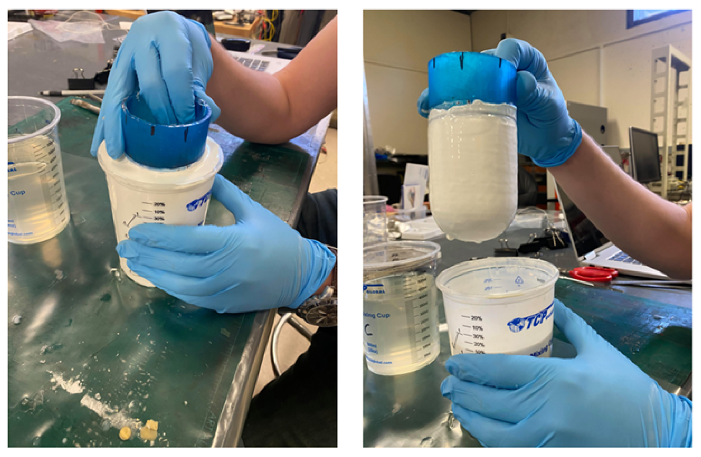
5.5. Coating Process
- A ceramic form is prepared for the dip process.
- The form is dipped in a liquid coagulant, allowing the latex to gel on the surface of the form in the next step.
- The coagulant-coated form is dipped into a vat of latex, which sets in combination with the coagulant on the surface of the form to a gel-like consistency. The form is allowed to reside in the latex vat for some time, depending on the desired latex thickness.
- The latex-coated form is “leached” by dipping it into a hot water tank, where it resides until all undesirable proteins are removed from the latex skin.
- The leached latex skin is dried in an oven below the curing temperature of the latex to remove excess moisture.
- The dried latex skin is cured in an oven, forming the desired latex article.
- The article is inverted from the form and is ready for use.
- Rather than a ceramic form, a 3-D printed form is used.
- The leaching step is removed so as to minimize the risk of damage to the embedded electronics.
- The curing schedule is performed at a lower temperature for a longer time to prevent the conductive epoxy in the PZT devices from flowing.
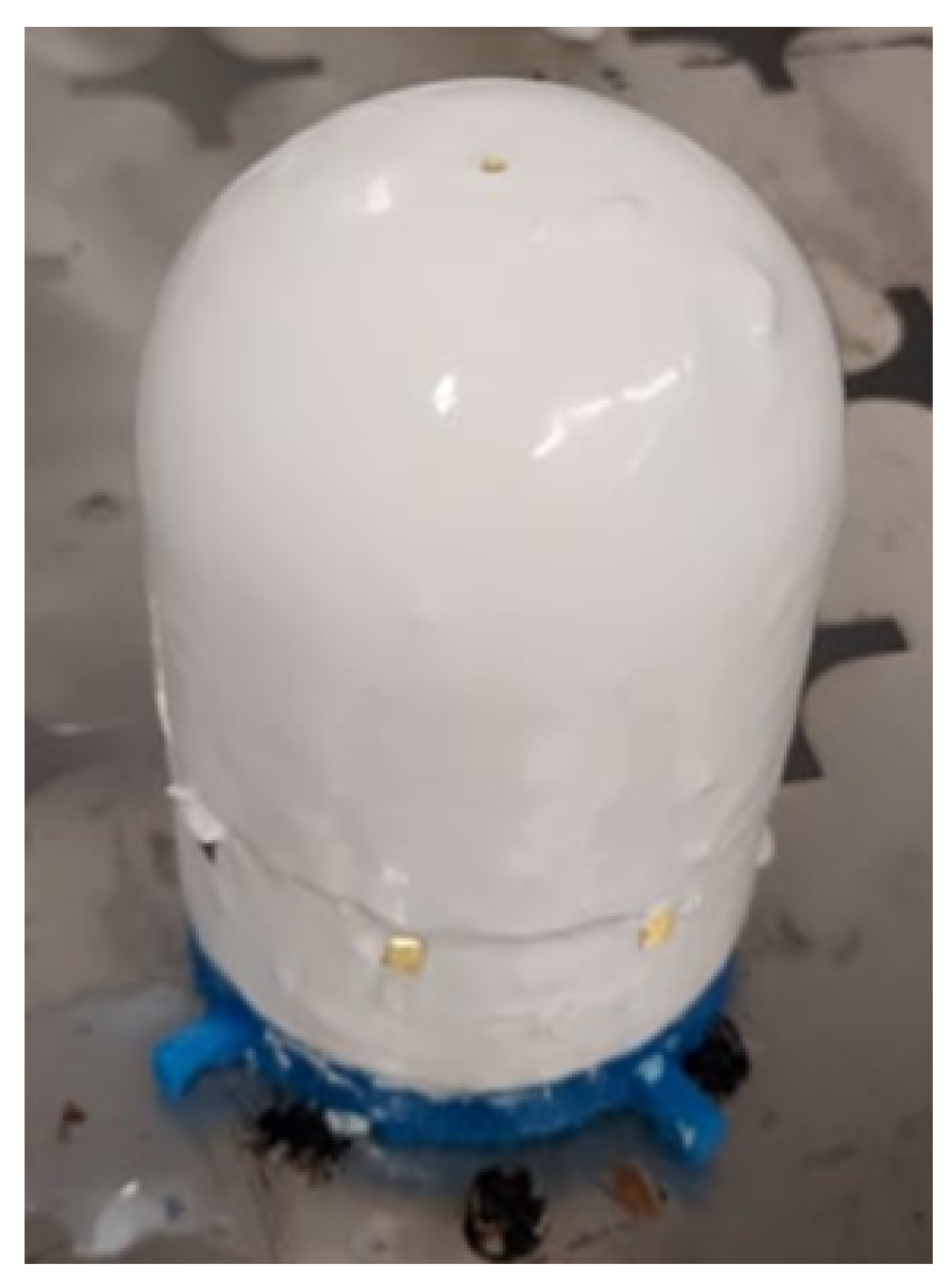
- Two successive coats are used to enclose the SSN, heretofore referred to as the “base” (first) and “top” (second) coats.
5.5.1. Base Coat Dip
5.5.2. Sensor Network Deployment
5.5.3. Topcoat Dip
5.5.4. Curing
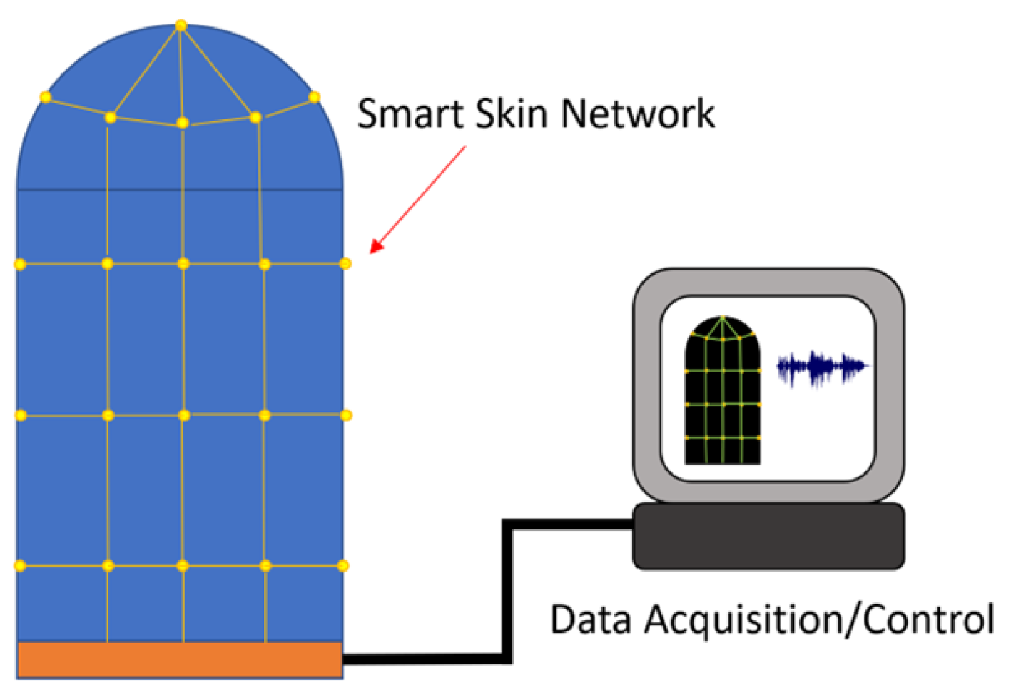
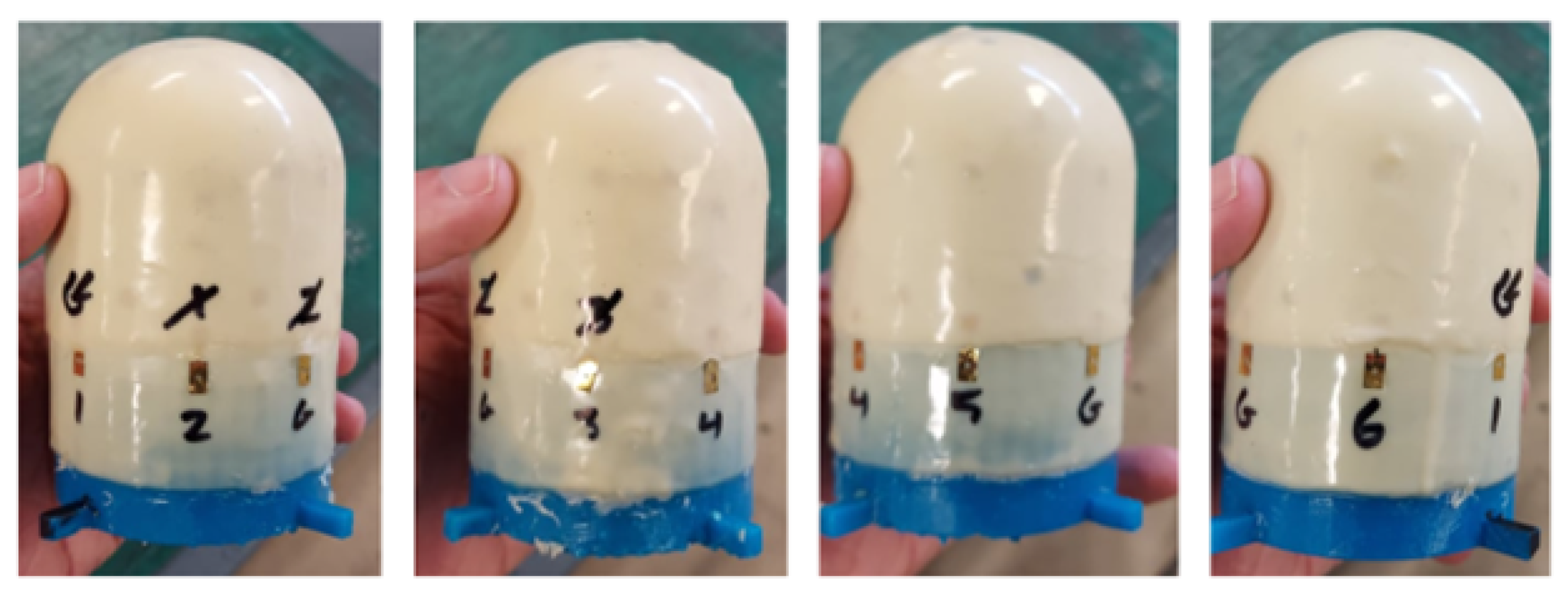
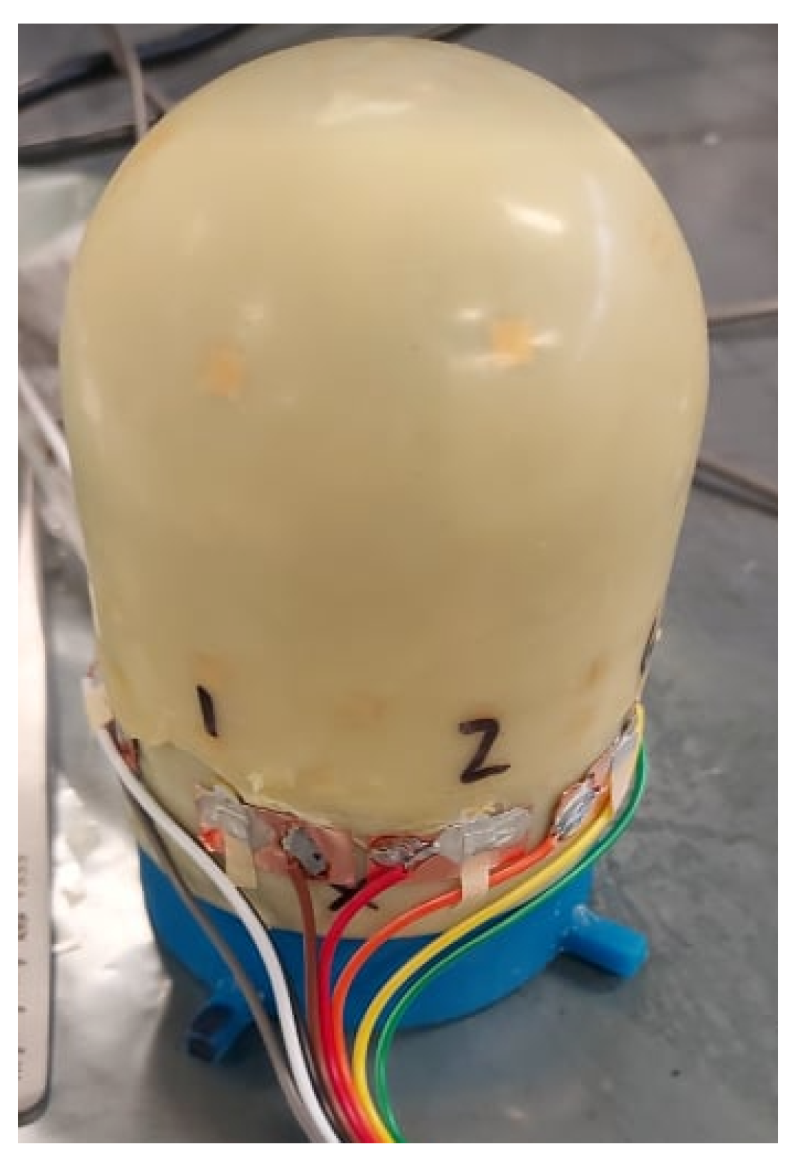
5.6. Integration
- A piece of copper tape was placed on the base coat of the latex underneath each signal pad. Each piece of copper tape would accommodated attachments to the edge pad and ribbon cable wire.
- Each edge pad was attached to its respective copper tape piece through painting using silver paste.
- One side of the ribbon cable wire was stripped. These wires were cut to shape to accommodate the curvature of the form.
- Each ribbon cable wire end was attached to its respective copper tape piece via soldering.
6. Results
6.1. RTD Validation
- The smart skin assembly was placed in a large oven to allow for a temperature-controlled environment. The assembly was plugged into a data acquisition unit through a voltage divider circuit by wiring it through an orifice in the rear of the oven.
- The oven was set to a prescribed set point.
- The resistance across each RTD element was calculated from the voltage divider circuit using a LabVIEW GUI and recorded.
6.2. PZT Validation
7. Conclusions
- A physics-based particle swarm optimization method was used to design the SSN, selecting the correct wire stiffness values for accurate deployment.
- A specialized tool was developed to expand and deploy the network from its fabricated footprint onto the target object.
- Materials were surveyed for use in the skin, and a dip-coating method was designed and implemented to form the skin layer.
- The skin was integrated with a data acquisition unit, and sensor functionality was validated.
Future Work
Author Contributions
Funding
Institutional Review Board Statement
Informed Consent Statement
Data Availability Statement
Acknowledgments
Conflicts of Interest
Abbreviations
| SACL | Structures and Composites Lab; |
| SNF | Stanford Nanofabrication Facility; |
| RTD | Resistance Temperature Detector; |
| PZT | Lead Zirconate Titanate (Transducer); |
| PSO | Particle Swarm Optimization. |
References
- Suleman, A.; Prasad, E.; Blackow, R.; Waechter, D. Smart Structures—An Overview; Springer: Berlin/Heidelberg, Germany, 2001; Volume 429, pp. 3–16. [Google Scholar] [CrossRef]
- Qiu, L.; Deng, X.; Yuan, S.; Huang, Y.; Ren, Y. Impact monitoring for aircraft smart composite skins based on a lightweight sensor network and characteristic digital sequences. Sensors 2018, 18, 2218. [Google Scholar] [CrossRef]
- Salmanpour, M.S.; Khodaei, Z.S.; Aliabadi, M.H.F. Impact damage localisation with piezoelectric sensors under operational and environmental conditions. Sensors 2017, 17, 1178. [Google Scholar] [CrossRef]
- Zhang, Y.; Xu, S.; Fu, H.; Lee, J.; Su, J.; Hwang, K.C.; Rogers, J.A.; Huang, Y. Buckling in serpentine microstructures and applications in elastomer-supported ultra-stretchable electronics with high areal coverage. Soft Matter 2013, 9, 8062–8070. [Google Scholar] [CrossRef]
- Qiu, L.; Yuan, S.; Shi, X.; Huang, T. Design of piezoelectric transducer layer with electromagnetic shielding and high connection reliability. Smart Mater. Struct. 2012, 21, 075032. [Google Scholar] [CrossRef]
- Roselli, L.; Carvalho, N.B.; Alimenti, F.; Mezzanotte, P.; Orecchini, G.; Virili, M.; Mariotti, C.; Goncalves, R.; Pinho, P. Smart surfaces: Large area electronics systems for internet of things enabled by energy harvesting. Proc. IEEE 2014, 102, 1723–1746. [Google Scholar] [CrossRef]
- Wang, Y.; Qiu, L.; Luo, Y.; Ding, R. A stretchable and large-scale guided wave sensor network for aircraft smart skin of structural health monitoring. Struct. Health Monit. 2019, 20, 861–876. [Google Scholar] [CrossRef]
- Yao, G.; Xu, L.; Cheng, X.; Li, Y.; Huang, X.; Guo, W.; Liu, S.; Wang, Z.L.; Wu, H. Bioinspired Triboelectric Nanogenerators as Self-Powered Electronic Skin for Robotic Tactile Sensing. Adv. Funct. Mater. 2020, 30, 1907312. [Google Scholar] [CrossRef]
- Hu, Y.; Rieutort-Louis, W.S.; Sanz-Robinson, J.; Huang, L.; Glisic, B.; Sturm, J.C.; Wagner, S.; Verma, N. Large-scale sensing system combining large-area electronics and cmos ics for structural-health monitoring. IEEE J. Solid-State Circuits 2014, 49, 513–523. [Google Scholar] [CrossRef]
- Guo, Z.; Aboudi, U.; Peumans, P.; Howe, R.T.; Chang, F.K. A Super Stretchable Organic Thin-Film Diodes Network That Can Be Embedded into Carbon Fiber Composite Materials for Sensor Network Applications. J. Microelectromech. Syst. 2016, 25, 524–532. [Google Scholar] [CrossRef]
- Salowitz, N.; Guo, Z.; Li, Y.H.; Kim, K.; Lanzara, G.; Chang, F.K. Bio-inspired stretchable network-based intelligent composites. J. Compos. Mater. 2013, 47, 97–105. [Google Scholar] [CrossRef]
- Gutbrod, S.R.; Sulkin, M.S.; Rogers, J.A.; Efimov, I.R. Patient-specific flexible and stretchable devices for cardiac diagnostics and therapy. Prog. Biophys. Mol. Biol. 2014, 115, 244–251. [Google Scholar] [CrossRef]
- Hu, Y.; Huang, L.; Rieutort-Louis, W.S.; Sanz-Robinson, J.; Sturm, J.C.; Wagner, S.; Verma, N. A self-powered system for large-scale strain sensing by combining CMOS ICs with large-area electronics. IEEE J. Solid-State Circuits 2014, 49, 838–850. [Google Scholar] [CrossRef]
- Takamiya, M.; Fuketa, H.; Ishida, K.; Yokota, T.; Sekitani, T.; Someya, T.; Sakurai, T. Flexible, large-area, and distributed organic electronics closely contacted with skin for healthcare applications. In Proceedings of the 2014 IEEE 57th International Midwest Symposium on Circuits and Systems (MWSCAS), College Station, TX, USA, 3–6 August 2014; pp. 829–832. [Google Scholar] [CrossRef]
- Dario, P.; Laschi, C.; Micera, S.; Vecchi, F.; Zecca, M.; Menciassi, A.; Mazzolai, B.; Carrozza, M.C. Biologically-Inspired Microfabricated Force and Position Mechano-Sensors; Springer: Vienna, Austria, 2003; pp. 109–125. [Google Scholar] [CrossRef]
- Sun, G.; Wu, Y.; Li, H.; Zhu, L. 3D shape sensing of flexible morphing wing using fiber Bragg grating sensing method. Optik 2018, 156, 83–92. [Google Scholar] [CrossRef]
- Sareh, S.; Jiang, A.; Faragasso, A.; Noh, Y.; Nanayakkara, T.; Dasgupta, P.; Seneviratne, L.D.; Wurdemann, H.A.; Althoefer, K. Bio-inspired tactile sensor sleeve for surgical soft manipulators. In Proceedings of the IEEE International Conference on Robotics and Automation, Hong Kong, China, 31 May–7 June 2014; pp. 1454–1459. [Google Scholar] [CrossRef]
- Wu, Y.; Liu, Y.; Zhou, Y.; Man, Q.; Hu, C.; Asghar, W.; Li, F.; Yu, Z.; Shang, J.; Liu, G.; et al. A skin-inspired tactile sensor for smart prosthetics. Sci. Robot. 2018, 3, eaat0429. [Google Scholar] [CrossRef]
- Wu, G.; Du, H.; Cha, Y.L.; Lee, D.; Kim, W.; Feyzbar-Khalkhali-Nejad, F.; Oh, T.S.; Zhang, X.; Kim, D.J. A wearable mask sensor based on polyaniline/CNT nanocomposites for monitoring ammonia gas and human breathing. Sens. Actuators B Chem. 2023, 375, 132858. [Google Scholar] [CrossRef]
- Wang, Z.; Bu, M.; Hu, N.; Zhao, L. An overview on room-temperature chemiresistor gas sensors based on 2D materials: Research status and challenge. Compos. Part B Eng. 2023, 248, 110378. [Google Scholar] [CrossRef]
- Yi, N.; Shen, M.; Erdely, D.; Cheng, H. Stretchable gas sensors for detecting biomarkers from humans and exposed environments. TrAC—Trends Anal. Chem. 2020, 133, 116085. [Google Scholar] [CrossRef]
- Wang, X.; Tao, L.; Yuan, M.; Wang, Z.; Yu, J.; Xie, D.; Luo, F.; Chen, X.; Wong, C.P. Sea urchin-like microstructure pressure sensors with an ultra-broad range and high sensitivity. Nat. Commun. 2021, 12, 1776. [Google Scholar] [CrossRef]
- Liu, C.; Qiao, H.; Su, J.; Zhang, P. Vision-based 3-D grasping of 3-D objects with a simple 2-D gripper. IEEE Trans. Syst. Man Cybern. Syst. 2014, 44, 605–620. [Google Scholar] [CrossRef]
- Cheng, Y.; Su, C.; Jia, Y.; Xi, N. Data Correlation Approach for Slippage Detection in Robotic Manipulations Using Tactile Sensor Array; Institute of Electrical and Electronics Engineers Inc.: Piscataway, NJ, USA, 2015; Volume 2015, pp. 2717–2722. [Google Scholar] [CrossRef]
- Zhang, C.; Liu, S.; Huang, X.; Guo, W.; Li, Y.; Wu, H. A stretchable dual-mode sensor array for multifunctional robotic electronic skin. Nano Energy 2019, 62, 164–170. [Google Scholar] [CrossRef]
- Luo, X.; Li, H.; Cao, D.; Dai, F.; Seo, J.; Lee, S. Recognizing Diverse Construction Activities in Site Images via Relevance Networks of Construction-Related Objects Detected by Convolutional Neural Networks. J. Comput. Civ. Eng. 2018, 32, 04018012. [Google Scholar] [CrossRef]
- Bekiroglu, Y.; Kragic, D.; Kyrki, V. Learning grasp stability based on tactile data and HMMs. In Proceedings of the 19th International Symposium in Robot and Human Interactive Communication, Viareggio, Italy, 13–15 September 2010; pp. 132–137. [Google Scholar] [CrossRef]
- Huang, S.; Wu, H. Texture recognition based on perception data from a bionic tactile sensor. Sensors 2021, 21, 5224. [Google Scholar] [CrossRef]
- Kopsaftopoulos, F.; Nardari, R.; Li, Y.H.; Chang, F.K. Data-driven State Awareness for Fly-by-feel Aerial Vehicles: Experimental Assessment of a Non-parametric Probabilistic Stall Detection Approach. Struct. Health Monit. 2017, 1595–1604. [Google Scholar] [CrossRef]
- Schmitz, A.; Maggiali, M.; Natale, L.; Bonino, B.; Metta, G. A tactile sensor for the fingertips of the humanoid robot iCub. In Proceedings of the 2010 IEEE/RSJ International Conference on Intelligent Robots and Systems, Taipei, Taiwan, 18–22 October 2010; pp. 2212–2217. [Google Scholar] [CrossRef]
- Maiolino, P.; Ascia, A.; Maggiali, M.; Natale, L.; Cannata, G.; Mett, G. Large Scale Capacitive Skin for Robots; InTech: London, UK, 2012. [Google Scholar] [CrossRef]
- Sun, X.; Sun, J.; Li, T.; Zheng, S.; Wang, C.; Tan, W.; Zhang, J.; Liu, C.; Ma, T.; Qi, Z.; et al. Flexible Tactile Electronic Skin Sensor with 3D Force Detection Based on Porous CNTs/PDMS Nanocomposites. Nano-Micro Lett. 2019, 11, 57. [Google Scholar] [CrossRef]
- Khan, S.; Lorenzelli, L.; Dahiya, R.S. Technologies for printing sensors and electronics over large flexible substrates: A review. IEEE Sens. J. 2015, 15, 3164–3185. [Google Scholar] [CrossRef]
- Guo, Z.; Kim, K.; Lanzara, G.; Salowitz, N.; Peumans, P.; Chang, F.K. Micro-fabricated, expandable temperature sensor network for macro-scale deployment in composite structures. In Proceedings of the IEEE Aerospace Conference Proceedings, Big Sky, MT, USA, 5–12 March 2011. [Google Scholar] [CrossRef]
- Clerc, M. Particle Swarm Optimization, 1st ed.; John Wiley & Sons: Hoboken, NJ, USA, 2010. [Google Scholar]
- Poli, R.; Kennedy, J.; Blackwell, T. Particle swarm optimization. Swarm Intell. 2007, 1, 33–57. [Google Scholar] [CrossRef]


Disclaimer/Publisher’s Note: The statements, opinions and data contained in all publications are solely those of the individual author(s) and contributor(s) and not of MDPI and/or the editor(s). MDPI and/or the editor(s) disclaim responsibility for any injury to people or property resulting from any ideas, methods, instructions or products referred to in the content. |
© 2024 by the authors. Licensee MDPI, Basel, Switzerland. This article is an open access article distributed under the terms and conditions of the Creative Commons Attribution (CC BY) license (https://creativecommons.org/licenses/by/4.0/).
Share and Cite
Ransom, E.; Chen, X.; Mangram, W.; Nasrollahi, A.; Topac, T.; Chang, F.-K. Design and Manufacture of Multifunctional 3-D Smart Skins with Embedded Sensor Networks for Robotic Applications. Sensors 2024, 24, 3441. https://doi.org/10.3390/s24113441
Ransom E, Chen X, Mangram W, Nasrollahi A, Topac T, Chang F-K. Design and Manufacture of Multifunctional 3-D Smart Skins with Embedded Sensor Networks for Robotic Applications. Sensors. 2024; 24(11):3441. https://doi.org/10.3390/s24113441
Chicago/Turabian StyleRansom, Elliot, Xiyuan Chen, William Mangram, Amir Nasrollahi, Tanay Topac, and Fu-Kuo Chang. 2024. "Design and Manufacture of Multifunctional 3-D Smart Skins with Embedded Sensor Networks for Robotic Applications" Sensors 24, no. 11: 3441. https://doi.org/10.3390/s24113441
APA StyleRansom, E., Chen, X., Mangram, W., Nasrollahi, A., Topac, T., & Chang, F.-K. (2024). Design and Manufacture of Multifunctional 3-D Smart Skins with Embedded Sensor Networks for Robotic Applications. Sensors, 24(11), 3441. https://doi.org/10.3390/s24113441