


A Fast and Low-Power Detection System for the Missing Pin Chip Based on YOLOv4-Tiny Algorithm


Abstract
1. Introduction
2. Experimental Setup
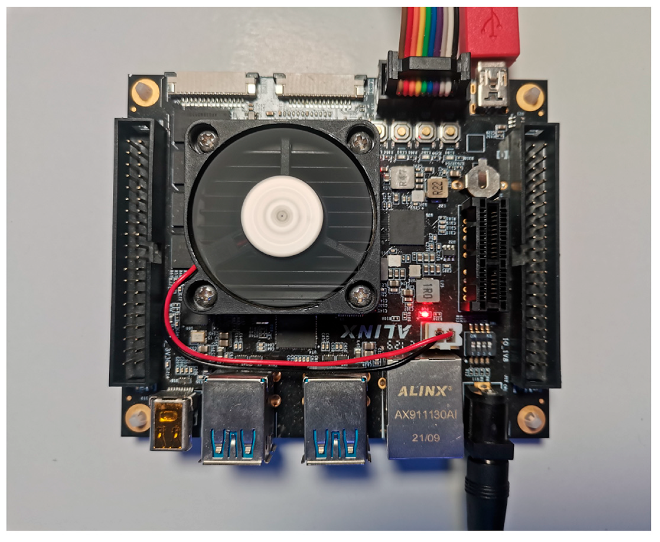
2.1. Experimental Platform
2.2. Development Tools
3. Theoretical Analysis
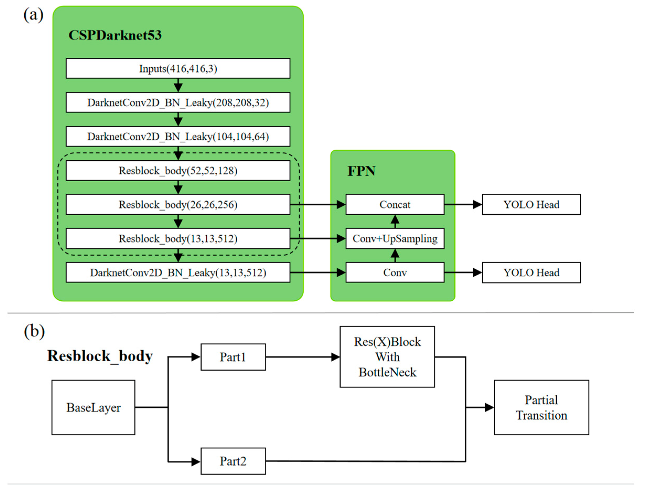
3.1. YOLOv4-Tiny Network
3.2. Fixed-Point 16-Bit Quantization
3.3. Fusion of the Batch Normalization (BN) Layer and Convolution Layer
3.4. Mean Average Precision (mAP) Derivation
4. Methods
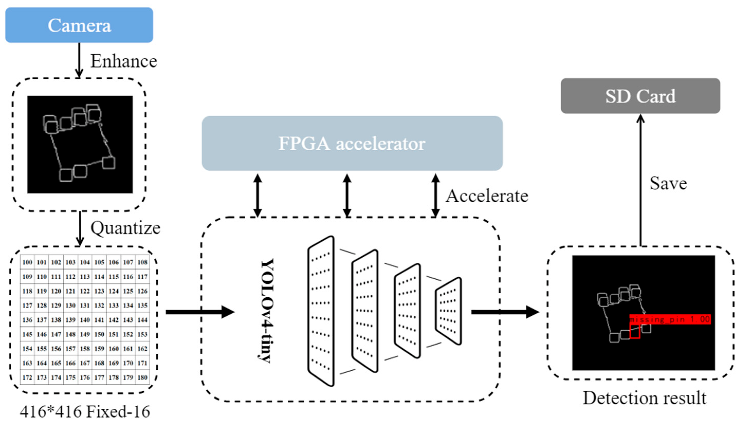
4.1. System Model
4.1.1. System Workflow
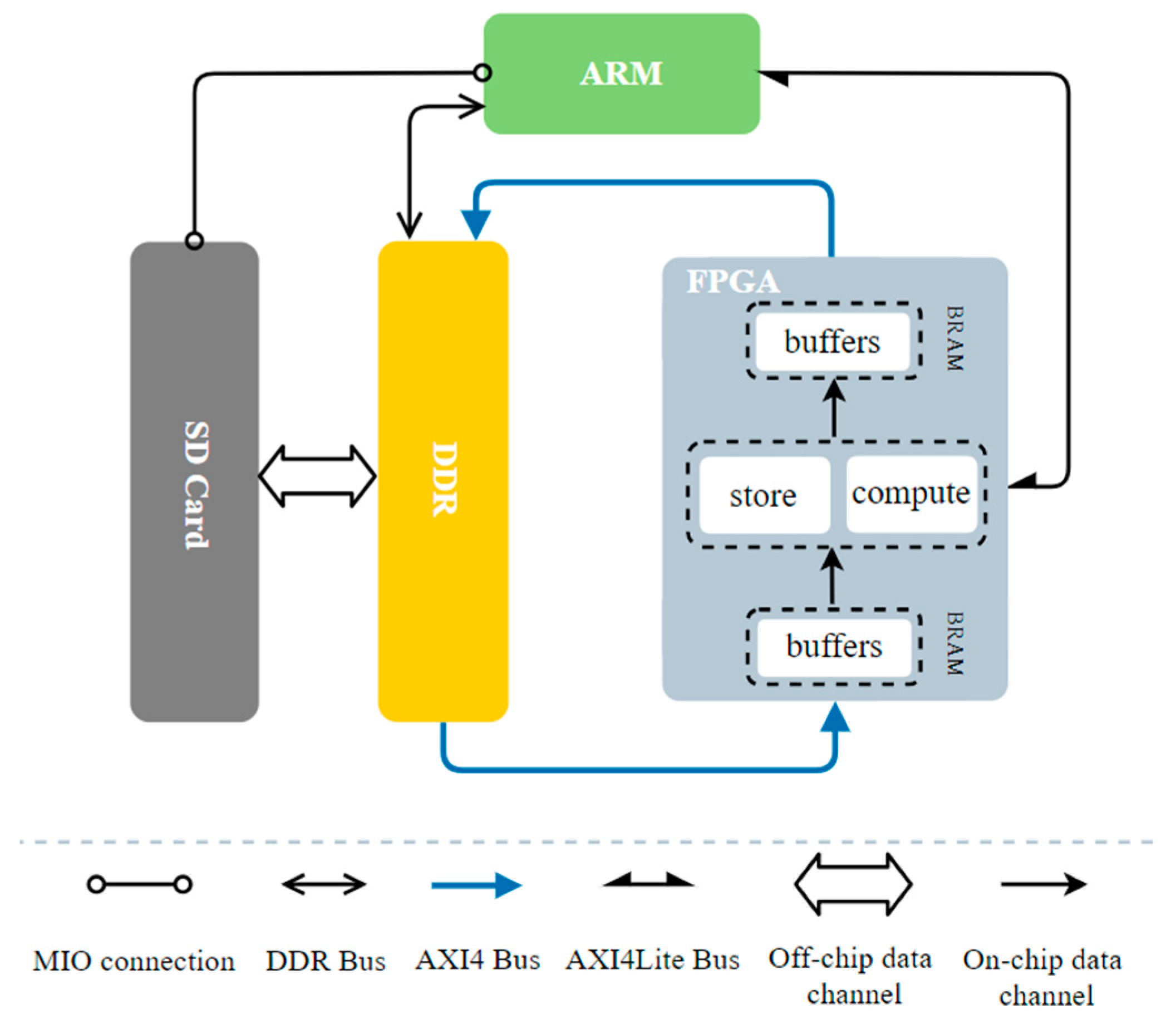
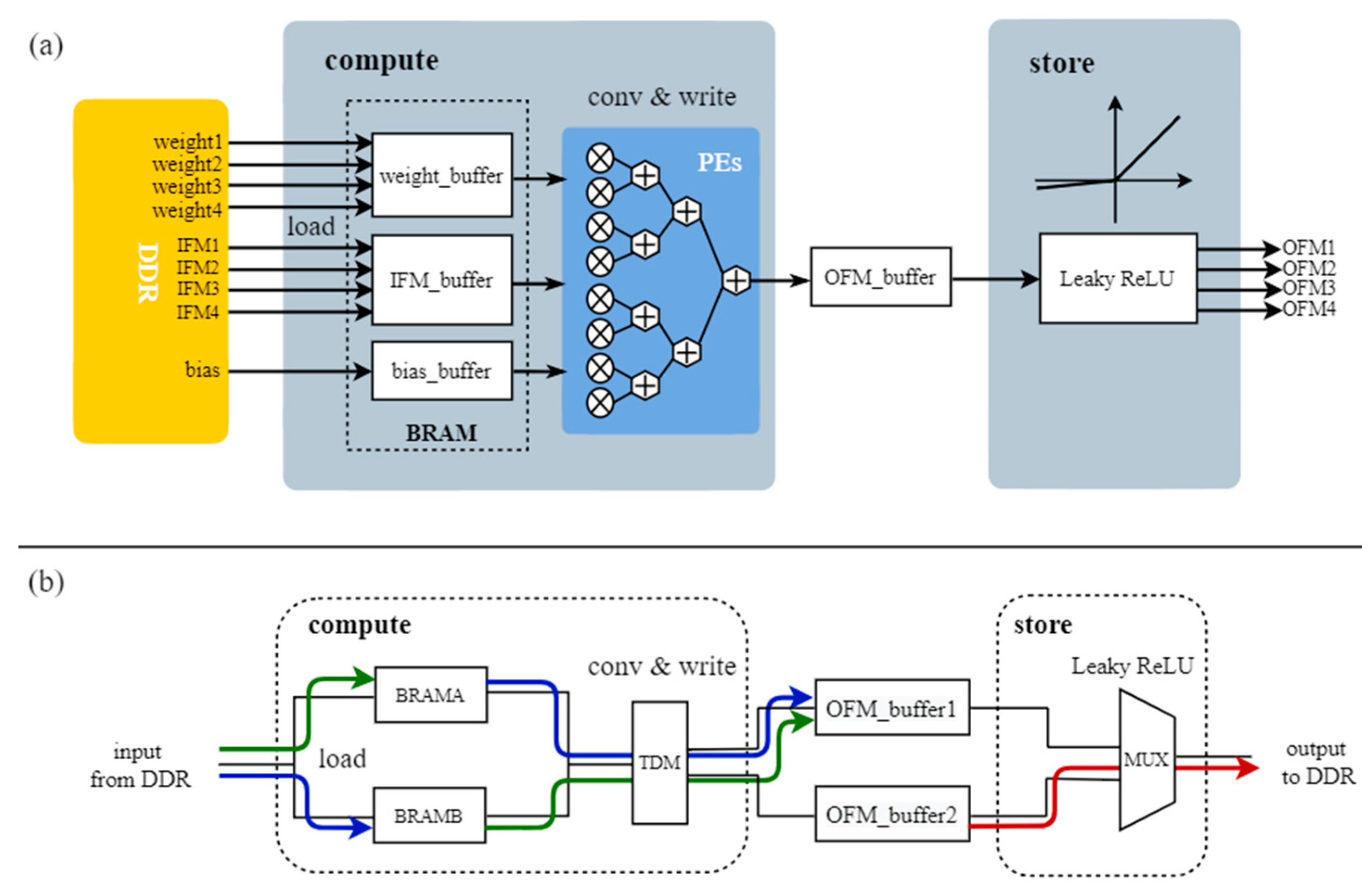
4.1.2. System Hardware Architecture
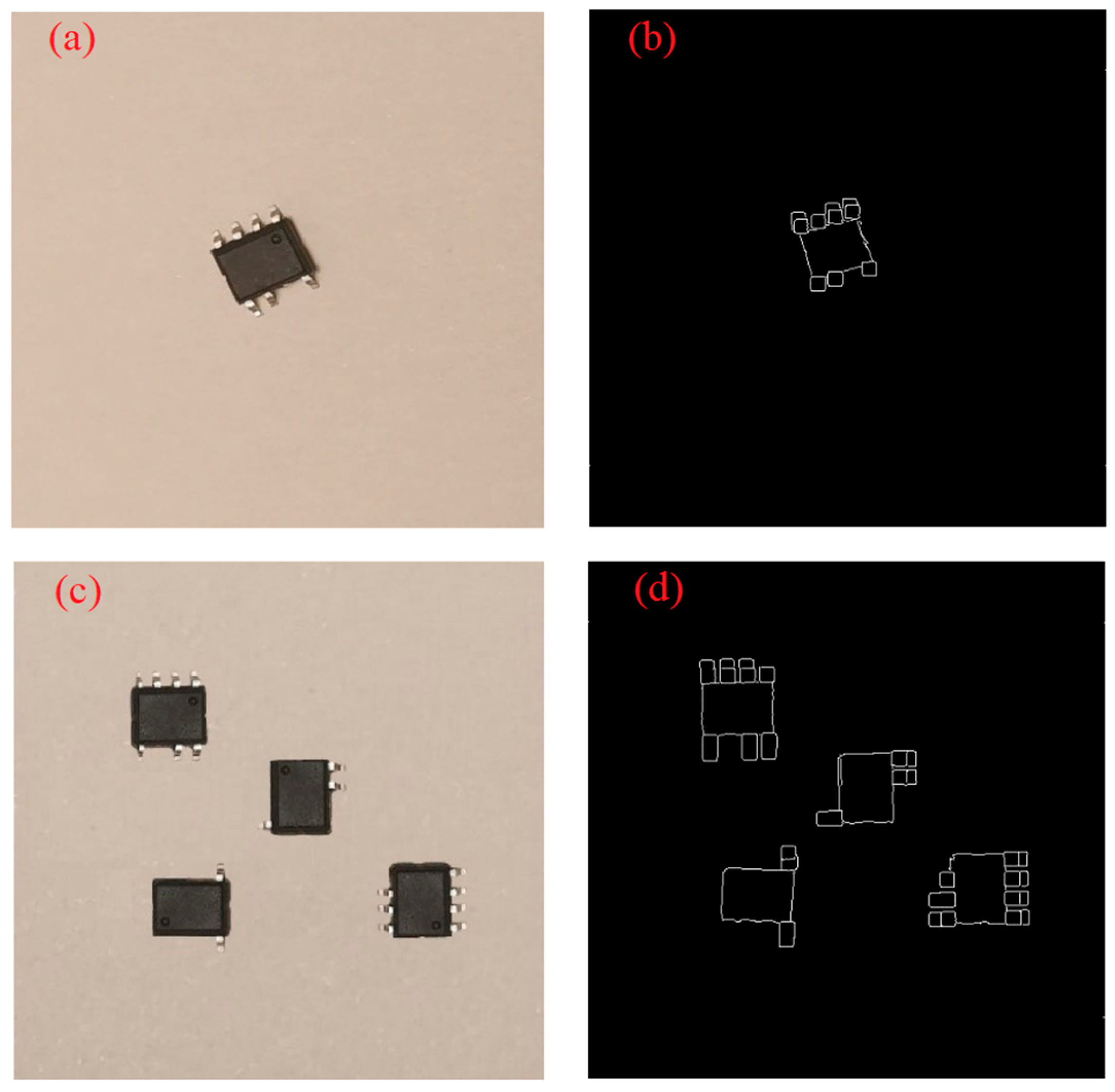
4.2. Dataset Enhancement
4.3. FPGA Deployment
4.3.1. Overall Design of the FPGA Accelerator
4.3.2. Detail Design of Convolution Kernel
| Algorithm 1 Pseudo code of optimized convolutional kernels |
| for (r = 0; r < R; r += Tr) {//Traverse the rows of the feature map in steps of Tr for (c = 0; c < C; c += Tc) {//Traverse the columns of the feature map in steps of Tm for (m = 0; m < M; m += Tm) {//Traverse the channels of the output feature map in steps of Tm for (n = 0; n < N; n += Tn) {//Traverse the channels of the input feature map in steps of Tn load I [n:n + Tn][r:r + Tr + K][c:c + Tc + K] to IFM_buffer; load W [m:m + Tm][n:n + Tn][:][:] to weight_buffer; //Compute partial sum and write to OFM_buffer for (ii = 0; ii < K; ii++)//Traverse the rows of the convolution kernel for (jj = 0; jj < K; jj++)//Traverse the columns of the convolution kernel for (rr = 0; rr < Tr; rr++)//Traverse the rows of the feature map block for (cc = 0; cc < Tc; cc++)//Traverse the columns of the feature map block #pragma HLS PIPELINE II = 1 for (mm = 0; mm < Tm; mm++)//Traverse the channels of the output feature map block for (nn = 0; nn < Tn; nn++)//Traverse the channels of the input feature map block OFM_buffer [mm][rr][cc]+= IFM_buffer [nn][rr + ii][cc + jj] × weight_buffer [mm][nn][ii][jj]; store OFM_buffer to O [m:m + Tm][r:r + Tr][c:c + Tc]; }}}} |
5. Results
5.1. Resource Consumption
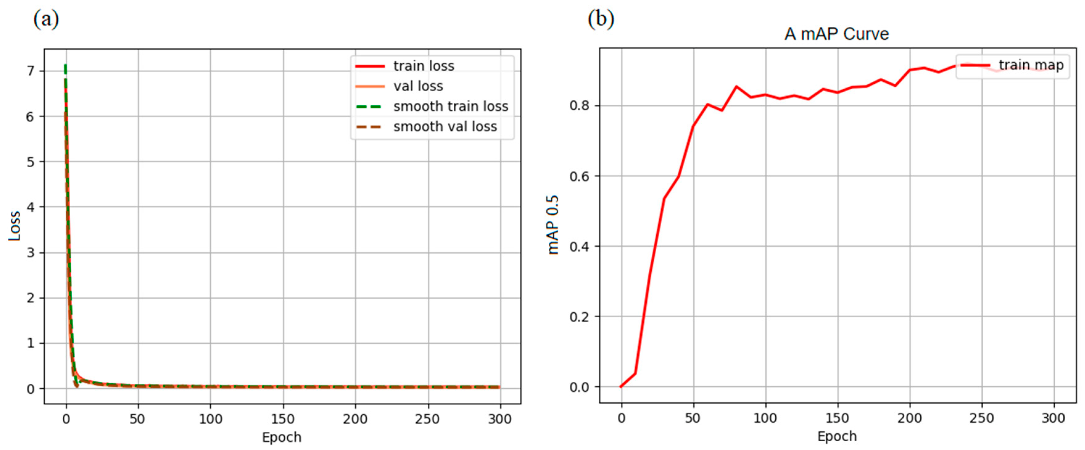
5.2. Model Training and Results
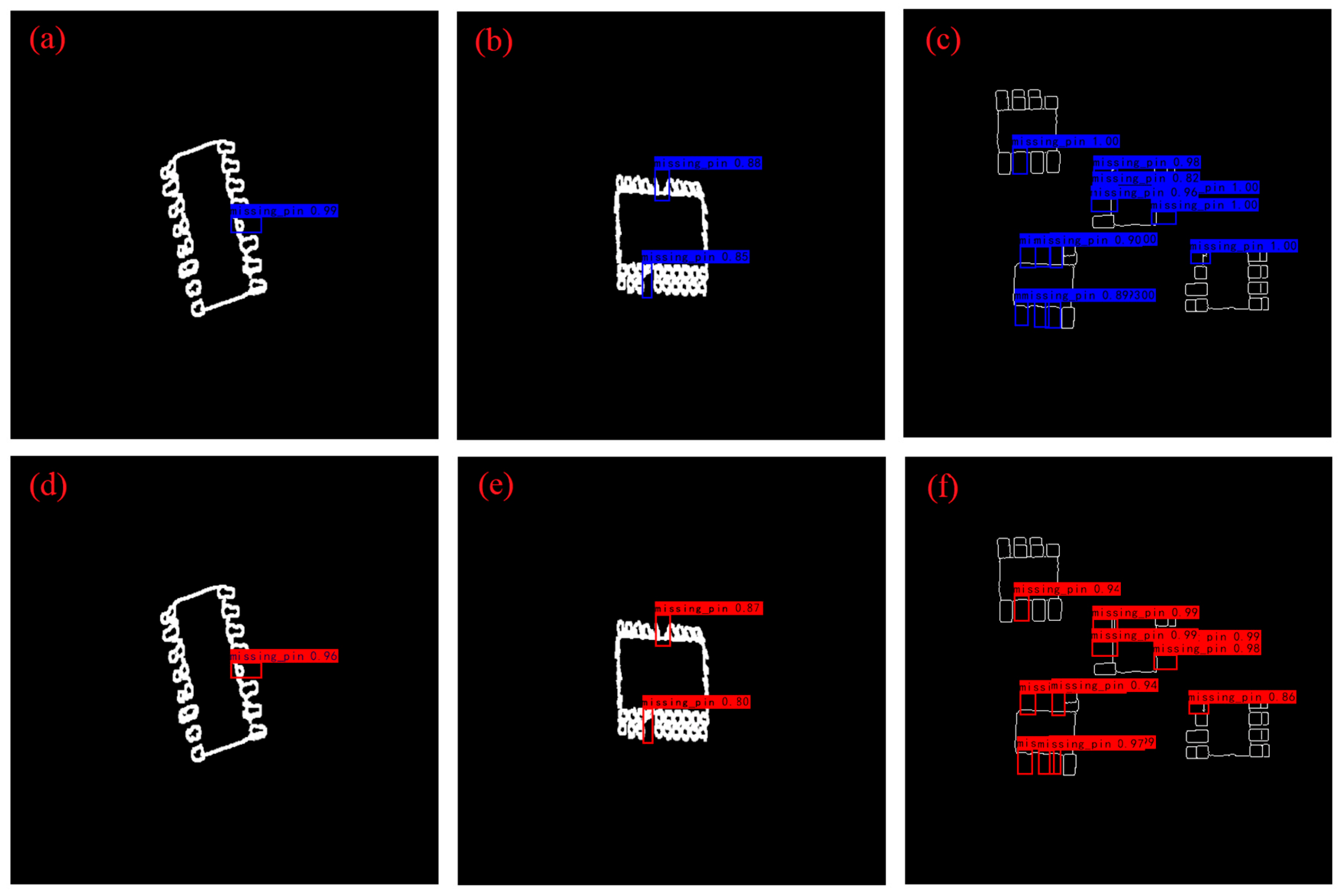
5.3. Inference Results
6. Comparison and Discussion
6.1. Comparison with Other Detection Solutions
6.2. Comparison with Other Platforms Deploying Neural Networks
6.3. Limitations and Potential Applications
- As neural networks grow more complex, richer FPGA resources are needed. To deploy a high-performing neural network on a resource-constrained FPGA, it is necessary to implement optimizations such as network compression and pruning to reduce the computational load and number of parameters.
- FPGA is not suitable for floating-point calculations, and quantization inevitably leads to reduced precision. A more fine-grained quantization scheme needs to be chosen to mitigate the impact of quantization on precision.
- This method primarily aims to detect chips in SOP packages. Since different chip packages may have distinct characteristics and specifications, the dataset requires extensive modification and augmentation, and the model must undergo rigorous training to ensure effective detection performance.
- The system can be combined with advanced sensors, Internet of Things (IoT) technology, and human-machine interaction technology to expand its application prospects.
- The target detection technology can be applied to high-precision, low-power consumption-demanding fields such as intelligent security, traffic safety, and autonomous driving, significantly improving production efficiency and reducing costs.
- This method provides an effective solution for deploying neural networks on FPGA and offers new ideas for the application of FPGA technology in the electronics industry.
7. Conclusions
- To improve the precision and FPGA computational performance, we preprocess image and weight files before feeding them into the YOLOv4-tiny network, using image enhancement, fixed-point 16-bit quantization, and the fusion of the BN layer and convolution layer.
- For the FPGA accelerator architecture, we design a two-layer ping-pong operation for uninterrupted read and write of off-chip memory DDR data. A loop tiling strategy is first used to cache feature blocks, and then the input and output channels are multiplexed in parallel to accelerate the convolution.
- The final result shows a precision of 89.33% on the AXU2CEG development board, which takes 0.468 s to process a single photo, consuming 3.52 W. Compared to a CPU platform, the time spent is reduced by 73.27%, and the power consumption is reduced to 23.08%. Moreover, the system can support multi-object detection scenarios, which greatly improves the detection efficiency.
Author Contributions
Funding
Institutional Review Board Statement
Informed Consent Statement
Data Availability Statement
Conflicts of Interest
Abbreviations
| mAP | mean average precision |
| CNN | convolutional neural network |
| FPN | feature pyramid network |
| BN | batch normalization |
| AP | average precision |
| TP | ture positives |
| FP | false positives |
| FN | false negatives |
| BRAM | block RAM |
| MIO | multiuse I/O |
| PEs | processing elements |
| TDM | time division multiplexing |
| IoT | internet of things |
References
- Fan, T.; Huang, D.; Tian, J.; Yu, S.; Wu, Z.; Dong, N. Research on height detection system based on machine vision element. Opt. Technol. 2020, 46, 102–109. [Google Scholar]
- Chen, J.; Zhang, Z.; Wu, F. A data-driven method for enhancing the image-based automatic inspection of IC wire bonding defects. Int. J. Prod. Res. 2021, 59, 4779–4793. [Google Scholar] [CrossRef]
- Song, J.; Kim, Y.; Park, T. SMT defect classification by feature extraction region optimization and machine learning. Int. J. Adv. Manuf. Technol. 2019, 101, 1303–1313. [Google Scholar] [CrossRef]
- Liu, C.; Chang, L. Characterization of surface micro-roughness by off-specular measurements of polarized optical scattering. Meas. Sci. Rev. 2019, 19, 257–263. [Google Scholar] [CrossRef]
- Jin, W.; Lin, W.; Yang, X.; Gao, H. Reference-free path-walking method for ball grid array inspection in surface mounting machines. IEEE Trans. Ind. Electron. 2017, 64, 6310–6318. [Google Scholar] [CrossRef]
- Liu, G.; Tong, H.; Li, Y.; Zhong, H.; Tan, Q. A profile shaping and surface finishing process of micro electrochemical machining for microstructures on microfluidic chip molds. Int. J. Adv. Manuf. Technol. 2021, 115, 1621–1636. [Google Scholar] [CrossRef]
- Liu, W.; Yang, X.; Yang, X.; Gao, H. A novel industrial chip parameters identification method based on cascaded region segmentation for surface-mount equipment. IEEE Trans. Ind. Electron. 2021, 69, 5247–5256. [Google Scholar] [CrossRef]
- Qiao, X.; Chen, T.; Zhuang, W.; Wu, J. A Chip Defect Detection System Based on Machine Vision. In Proceedings of the IncoME-VI and TEPEN 2021: Performance Engineering and Maintenance Engineering; Springer: Berlin/Heidelberg, Germany, 2022; pp. 555–568. [Google Scholar]
- Lu, S.; Zhang, J.; Hao, F.; Jiao, L. Automatic Detection of Chip Pin Defect in Semiconductor Assembly Using Vision Measurement. Meas. Sci. Rev. 2022, 22, 231–240. [Google Scholar] [CrossRef]
- Jiang, L.; Wang, Y.; Tang, Z.; Miao, Y.; Chen, S. Casting defect detection in X-ray images using convolutional neural networks and attention-guided data augmentation. Measurement 2021, 170, 108736. [Google Scholar] [CrossRef]
- Gao, M.; Song, P.; Wang, F.; Liu, J.; Mandelis, A.; Qi, D. A novel deep convolutional neural network based on ResNet-18 and transfer learning for detection of wood knot defects. J. Sensors 2021, 2021, 4428964. [Google Scholar] [CrossRef]
- Chen, Y.; Peng, X.; Kong, L.; Dong, G.; Remani, A.; Leach, R. Defect inspection technologies for additive manufacturing. Int. J. Extreme. Manuf. 2021, 3, 022002. [Google Scholar] [CrossRef]
- Wang, K.; Fan-Jiang, H.; Lee, Y. A multiple-stage defect detection model by convolutional neural network. Comput. Ind. Eng. 2022, 168, 108096. [Google Scholar] [CrossRef]
- Zhao, L.; Li, F.; Zhang, Y.; Xu, X.; Xiao, H.; Feng, Y. A deep-learning-based 3D defect quantitative inspection system in CC products surface. Sensors 2020, 20, 980. [Google Scholar] [CrossRef] [PubMed]
- Ding, R.; Dai, L.; Li, G.; Liu, H. TDD—Net: A tiny defect detection network for printed circuit boards. CAAI Trans. Intell. Technology 2019, 4, 110–116. [Google Scholar] [CrossRef]
- Yang, X.; Dong, F.; Liang, F.; Zhang, G. Chip defect detection based on deep learning method. In Proceedings of the 2021 IEEE International Conference on Power Electronics, Computer Applications (ICPECA, 2021), Shenyang, China, 22–24 January 2021; IEEE: Piscataway, NJ, USA, 2021; pp. 215–219. [Google Scholar]
- Ghosh, P.; Bhattacharya, A.; Forte, D.; Chakraborty, R.S. Automated defective pin detection for recycled microelectronics identification. J. Hardw. Syst. Secur. 2019, 3, 250–260. [Google Scholar] [CrossRef]
- Hou, D.; Liu, T.; Pan, Y.; Hou, J. AI on edge device for laser chip defect detection. In Proceedings of the 2019 IEEE 9th Annual Computing and Communication Workshop and Conference (CCWC), Las Vegas, NV, USA, 7–9 January 2019; IEEE: Piscataway, NJ, USA, 2019; pp. 0247–0251. [Google Scholar]
- Howell, L.; Anagnostidis, V.; Gielen, F. Multi—Object detector yolov4—Tiny enables high—Throughput combinatorial and spatially—Resolved sorting of cells in microdroplets. Adv. Mater. Technol. 2022, 7, 2101053. [Google Scholar] [CrossRef]
- Huang, H.; Liu, Z.; Chen, T.; Hu, X.; Zhang, Q.; Xiong, X. Design space exploration for yolo neural network accelerator. Electronics 2020, 9, 1921. [Google Scholar] [CrossRef]
- Kim, T.; Park, S.; Cho, Y. Study on the Implementation of a Simple and Effective Memory System for an AI Chip. Electronics 2021, 10, 1399. [Google Scholar] [CrossRef]
- Zhang, N.; Wei, X.; Chen, H.; Liu, W. FPGA implementation for CNN-based optical remote sensing object detection. Electronics 2021, 10, 282. [Google Scholar] [CrossRef]
- Yu, Y.; Wu, C.; Zhao, T.; Wang, K.; He, L. OPU: An FPGA-based overlay processor for convolutional neural networks. IEEE Trans. VLSI Syst. 2019, 28, 35–47. [Google Scholar] [CrossRef]
- Luo, Y.; Chen, Y. FPGA-based acceleration on additive manufacturing defects inspection. Sensors 2021, 21, 2123. [Google Scholar] [CrossRef]
- Adibhatla, V.A.; Chih, H.; Hsu, C.; Cheng, J.; Abbod, M.F.; Shieh, J. Defect detection in printed circuit boards using you-only-look-once convolutional neural networks. Electronics 2020, 9, 1547. [Google Scholar] [CrossRef]
- Adibhatla, V.A.; Chih, H.; Hsu, C.; Cheng, J.; Abbod, M.F.; Shieh, J. Applying deep learning to defect detection in printed circuit boards via a newest model of you-only-look-once. Math. Biosci. Eng. 2021, 18, 4411–4428. [Google Scholar] [CrossRef] [PubMed]
- Bing, W.; Wenjing, L.; Huan, T. Improved Yolo V3 algorithm and its application in helmet detection. Comput. Eng. Appl. 2020, 56, 33–40. [Google Scholar]
- Zhu, J.; Wang, J.L.; Wang, B. Lightweight mask detection algorithm based on improved YOLOv4-tiny. Chin. J. Liq. Cryst. Disp. 2021, 36, 1525–1534. [Google Scholar] [CrossRef]
- Young, S.I.; Zhe, W.; Taubman, D.; Girod, B. Transform quantization for cnn compression. IEEE Trans. Pattern Anal. Mach. Intell. 2021, 44, 5700–5714. [Google Scholar] [CrossRef]
- Jacob, B.; Kligys, S.; Chen, B.; Zhu, M.; Tang, M.; Howard, A.; Adam, H.; Kalenichenko, D. Quantization and training of neural networks for efficient integer-arithmetic-only inference. In Proceedings of the IEEE Conference on Computer Vision and Pattern Recognition, Salt Lake City, UT, USA, 18–23 June 2018; pp. 2704–2713. [Google Scholar]
- Nakata, K.; Miyashita, D.; Deguchi, J.; Fujimoto, R. Adaptive quantization method for CNN with computational-complexity-aware regularization. In Proceedings of the 2021 IEEE International Symposium on Circuits and Systems (ISCAS), Daegu, Republic of Korea, 22–28 May 2021; IEEE: Piscataway, NJ, USA, 2021; pp. 1–5. [Google Scholar]
- Genaev, M.A.; Komyshev, E.G.; Shishkina, O.D.; Adonyeva, N.V.; Karpova, E.K.; Gruntenko, N.E.; Zakharenko, L.P.; Koval, V.S.; Afonnikov, D.A. Classification of fruit flies by gender in images using smartphones and the YOLOv4-tiny neural network. Mathematics 2022, 10, 295. [Google Scholar] [CrossRef]
- Ling, Y.; Chin, H.; Wu, H.; Tsay, R. Designing a compact convolutional neural network processor on embedded fpgas. In Proceedings of the 2020 IEEE Global Conference on Artificial Intelligence and Internet of Things (GCAIoT), Dubai, United Arab Emirates, 12–16 December 2020; IEEE: Piscataway, NJ, USA, 2020; pp. 1–7. [Google Scholar]
- Gerhards, J.; Held, D.; Schneider, T.; Hirmer, P. Burst-a dynamic bus routing system. In Proceedings of the 2021 IEEE International Conference on Pervasive Computing and Communications Workshops and other Affiliated Events (PerCom Workshops), Kassel, Germany, 22–26 March 2021; IEEE: Piscataway, NJ, USA, 2021; pp. 395–397. [Google Scholar]
- Dwivedi, P.; Mishra, N.; Singh-Rajput, A. Assertion & Functional Coverage Driven Verification of AMBA Advance Peripheral Bus Protocol Using System Verilog. In Proceedings of the 2021 International Conference on Advances in Electrical, Computing, Communication and Sustainable Technologies (ICAECT), Bhilai, India, 19–20 February 2021; IEEE: Piscataway, NJ, USA, 2021; pp. 1–6. [Google Scholar]
- Qiu, J.; Wang, J.; Yao, S.; Guo, K.; Li, B.; Zhou, E.; Yu, J.; Tang, T.; Xu, N.; Song, S. Going deeper with embedded fpga platform for convolutional neural network. In Proceedings of the 2016 ACM/SIGDA International Symposium on Field-Programmable Gate Arrays, Monterey, CA, USA, 21–23 February 2016; pp. 26–35. [Google Scholar]
- Li, P.; Che, C. Mapping YOLOv4-Tiny on FPGA-Based DNN Accelerator by Using Dynamic Fixed-Point Method. In Proceedings of the 2021 12th International Symposium on Parallel Architectures, Algorithms and Programming (PAAP), Xi’an, China, 10–12 December 2021; IEEE: Piscataway, NJ, USA, 2021; pp. 125–129. [Google Scholar]
- Yu, Z.; Bouganis, C. A parameterisable FPGA-tailored architecture for YOLOv3-tiny. In Applied Reconfigurable Computing. Architectures, Tools, and Applications, Proceedings of the 16th International Symposium, ARC 2020, Toledo, Spain, 1–3 April 2020; Springer: Berlin/Heidelberg, Germany, 2020; pp. 330–344. [Google Scholar]
- Suda, N.; Chandra, V.; Dasika, G.; Mohanty, A.; Ma, Y.; Vrudhula, S.; Seo, J.; Cao, Y. Throughput-optimized OpenCL-based FPGA accelerator for large-scale convolutional neural networks. In Proceedings of the 2016 ACM/SIGDA International Symposium on Field-Programmable Gate Arrays, Monterey, CA, USA, 21–23 February 2016; pp. 16–25. [Google Scholar]


| Resource | LUT (47,232) | FF (94,464) | BRAM (150) | DSP (240) | /MHz |
|---|---|---|---|---|---|
| System consumption | 41,369 (87.6%) | 47,111 (49.9%) | 96 (64.0%) | 223 (92.9%) | 100 |
| Convolution consumption | 23,361 (49.5%) | 21,878 (23.2%) | 92 (61.3%) | 199 (82.9%) | 100 |
| Parameters | CPU | Paper [37] | Paper [38] | Paper [39] | This Paper |
|---|---|---|---|---|---|
| Experimental Platform | Core i5-10210U | Zedboard | Zedboard | Stratix V GSD8 | AXU2CGB |
| Quantization | Float-32 | Fixed-16 | Fixed-16 | Fixed-16 | Fixed-16 |
| Frequency/Hz | 1.6 G | 100 M | 100 M | 120 M | 100 M |
| Inference time per img/s | 1.751 | 18.025 | 0.532 | 0.651 | 0.468 |
| Mean average precision (mAP) | 90.76% | 69% | 30.9% | 87.48% | 89.33% |
| Power/W | 15.25 | 2.384 | 3.36 | 25.40 | 3.52 |
Disclaimer/Publisher’s Note: The statements, opinions and data contained in all publications are solely those of the individual author(s) and contributor(s) and not of MDPI and/or the editor(s). MDPI and/or the editor(s) disclaim responsibility for any injury to people or property resulting from any ideas, methods, instructions or products referred to in the content. |
© 2023 by the authors. Licensee MDPI, Basel, Switzerland. This article is an open access article distributed under the terms and conditions of the Creative Commons Attribution (CC BY) license (https://creativecommons.org/licenses/by/4.0/).
Share and Cite
Chen, S.; Lai, W.; Ye, J.; Ma, Y. A Fast and Low-Power Detection System for the Missing Pin Chip Based on YOLOv4-Tiny Algorithm. Sensors 2023, 23, 3918. https://doi.org/10.3390/s23083918
Chen S, Lai W, Ye J, Ma Y. A Fast and Low-Power Detection System for the Missing Pin Chip Based on YOLOv4-Tiny Algorithm. Sensors. 2023; 23(8):3918. https://doi.org/10.3390/s23083918
Chicago/Turabian StyleChen, Shiyi, Wugang Lai, Junjie Ye, and Yingjie Ma. 2023. "A Fast and Low-Power Detection System for the Missing Pin Chip Based on YOLOv4-Tiny Algorithm" Sensors 23, no. 8: 3918. https://doi.org/10.3390/s23083918
APA StyleChen, S., Lai, W., Ye, J., & Ma, Y. (2023). A Fast and Low-Power Detection System for the Missing Pin Chip Based on YOLOv4-Tiny Algorithm. Sensors, 23(8), 3918. https://doi.org/10.3390/s23083918