
Microwave Frequency Doubler with Improved Stabilization of Output Power


Abstract
:1. Introduction
2. Materials and Methods
- -
- Frequency multiplication order equal to N = 2;
- -
- Input frequency f = 1 GHz;
- -
- Stabilization of output power at second harmonics (2 GHz) within 1 dB range for at least 6 dB input power range (generally, as wide as possible).
- -
- Concept of the circuit;
- -
- Defining of the nonlinear model describing the circuit’s work;
- -
- Numerical calculations of output power;
- -
- Microwave design and nonlinear simulations with the use of AWR Microwave Office;
- -
- Circuit realization and measurements.
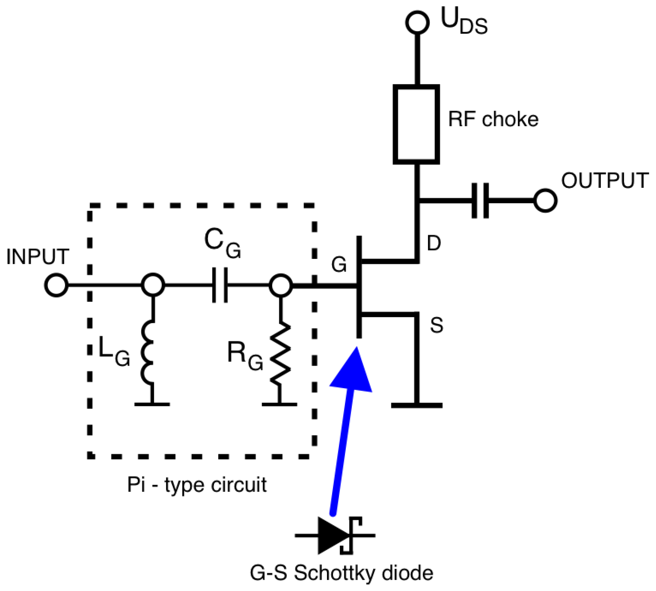
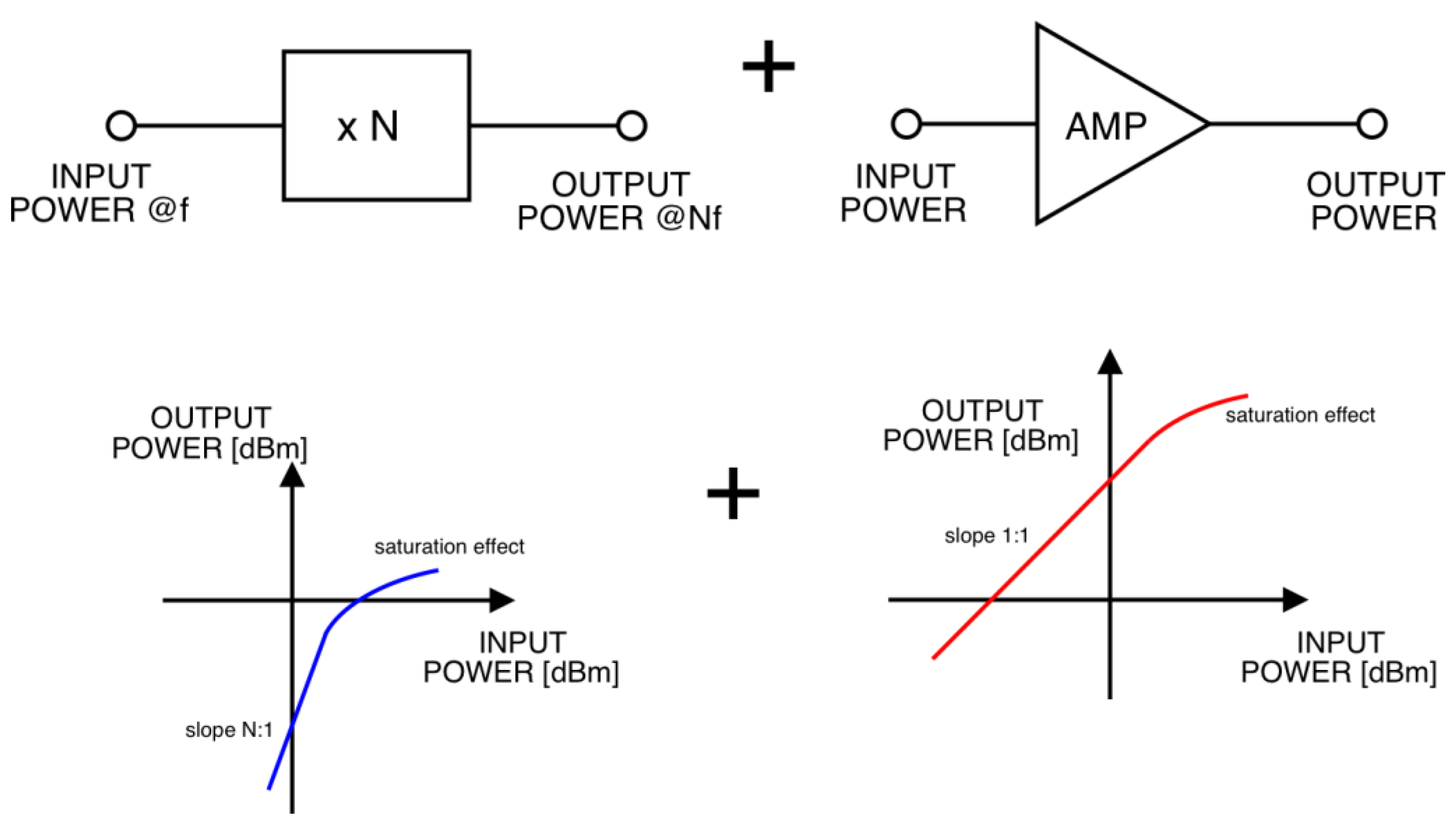
2.1. Concept
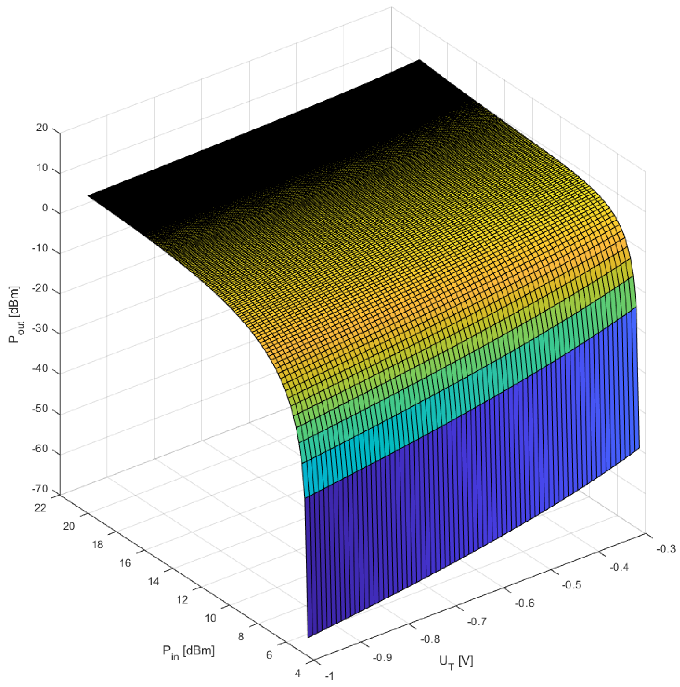
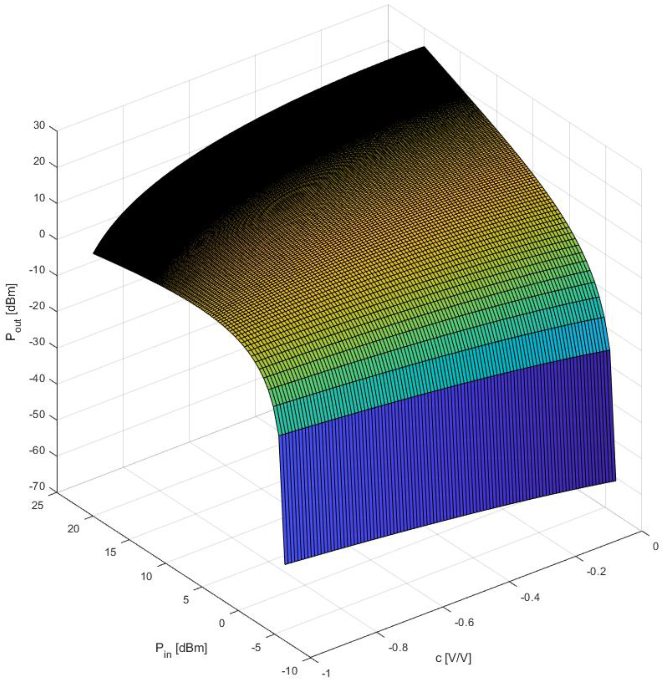
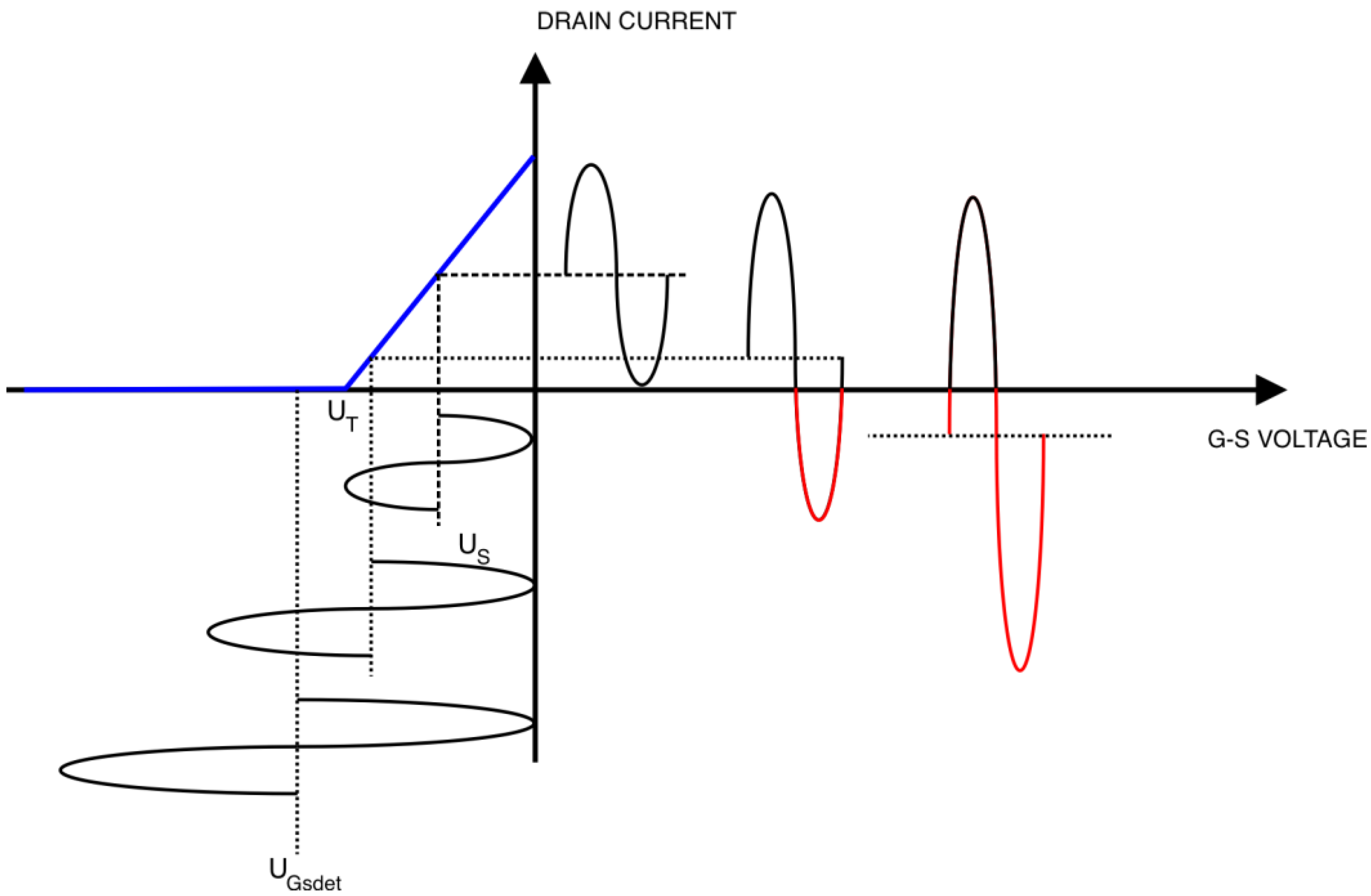
2.2. Modeling and Calculations
- ID0—value of drain current for gate-source voltage equal to zero,
- UT—transistor threshold voltage.
- c—detector coefficient [V/V].
- Usnlin—the value of the driving voltage amplitude for the non-linear range.
- -
- Constant detector coefficient c and variable threshold voltage UT;
- -
- Constant threshold voltage UT and variable detector coefficient c.
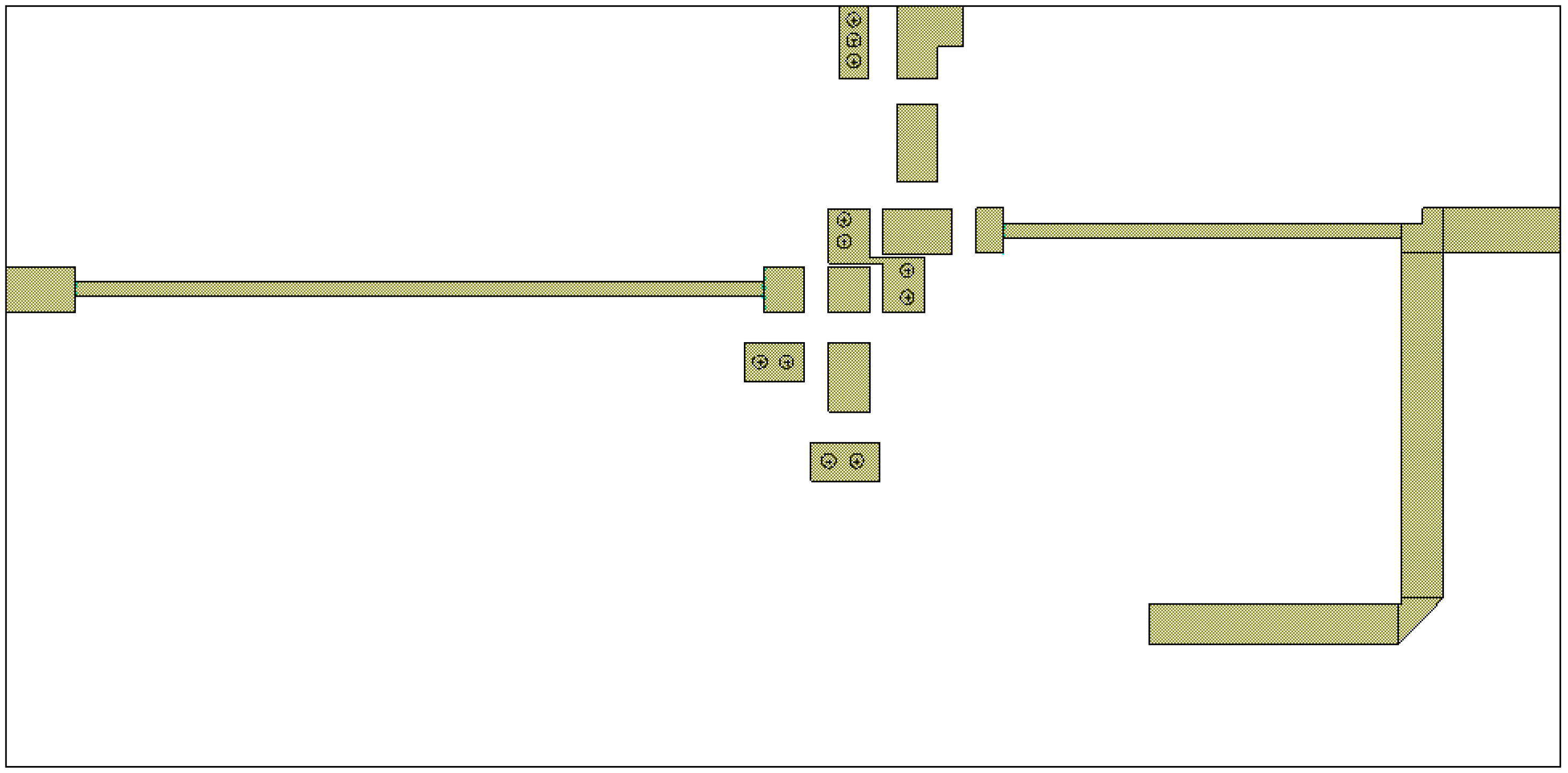
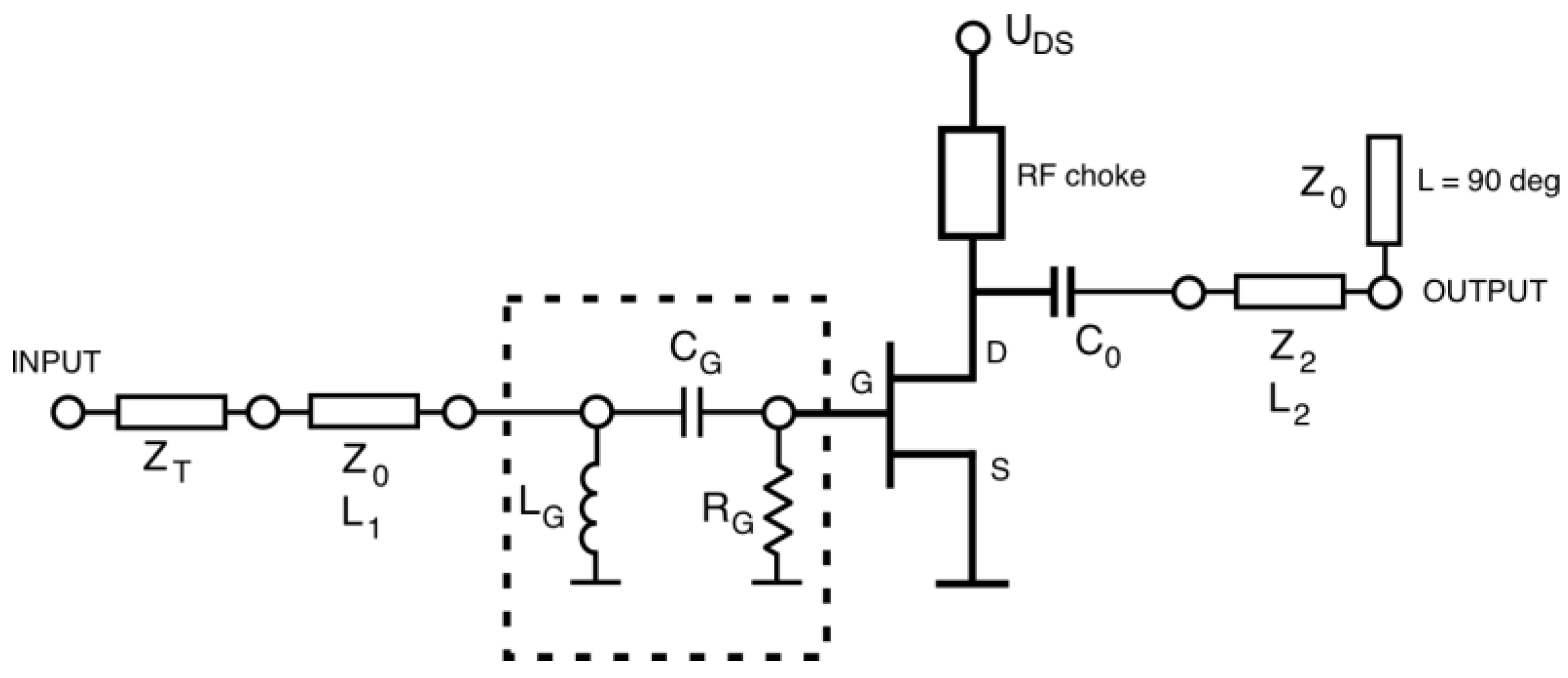
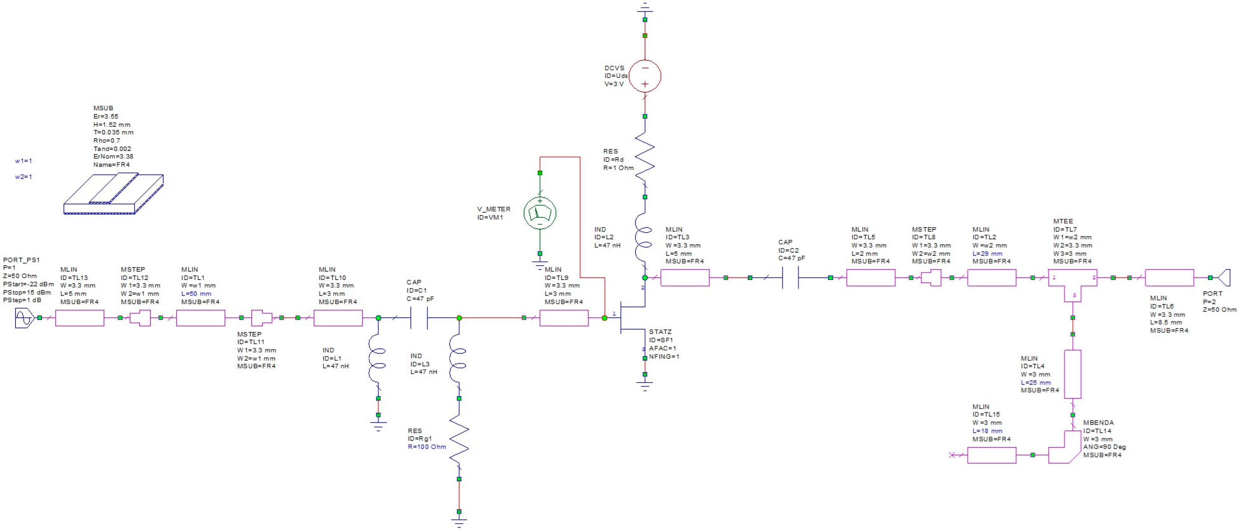
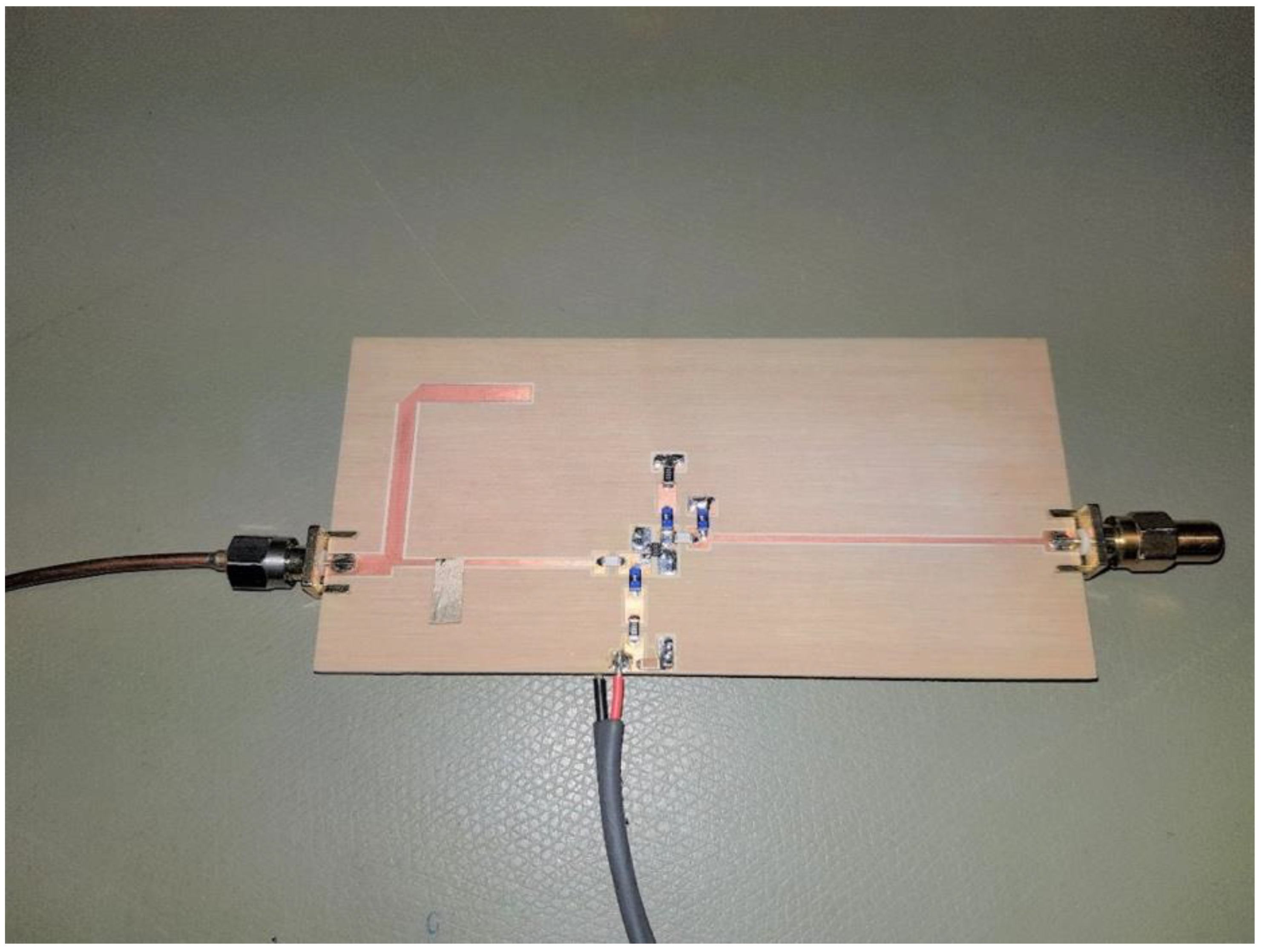
2.3. Circuit Design
- -
- CG = 47 pF, RG = 100 Ω, LG = 47 nH;
- -
- ZT = 150 Ω, L1 = 3 mm (FR-4 laminate), L2 = 29 mm (FR-4 laminate);
- -
- UDS = 3 V.
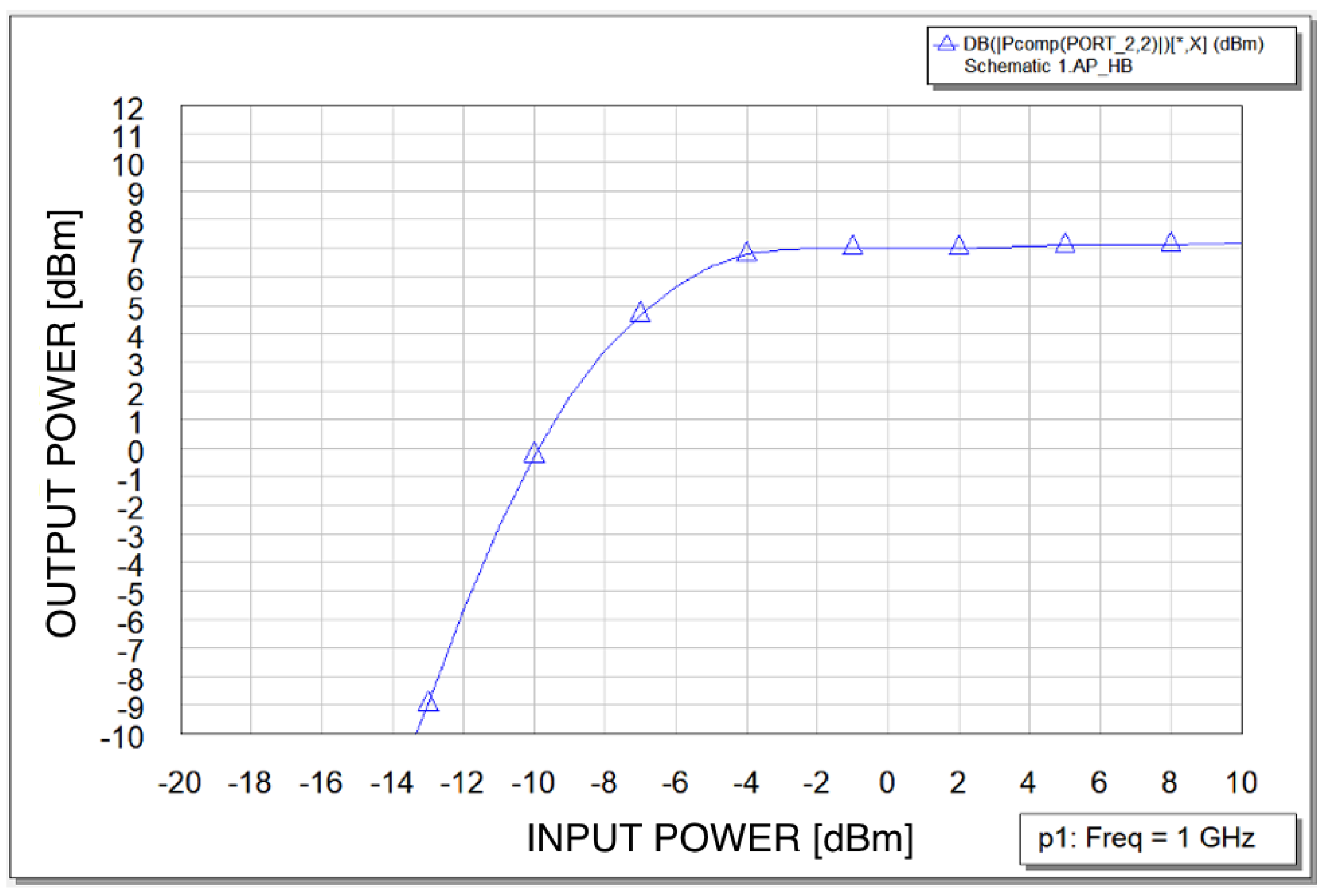
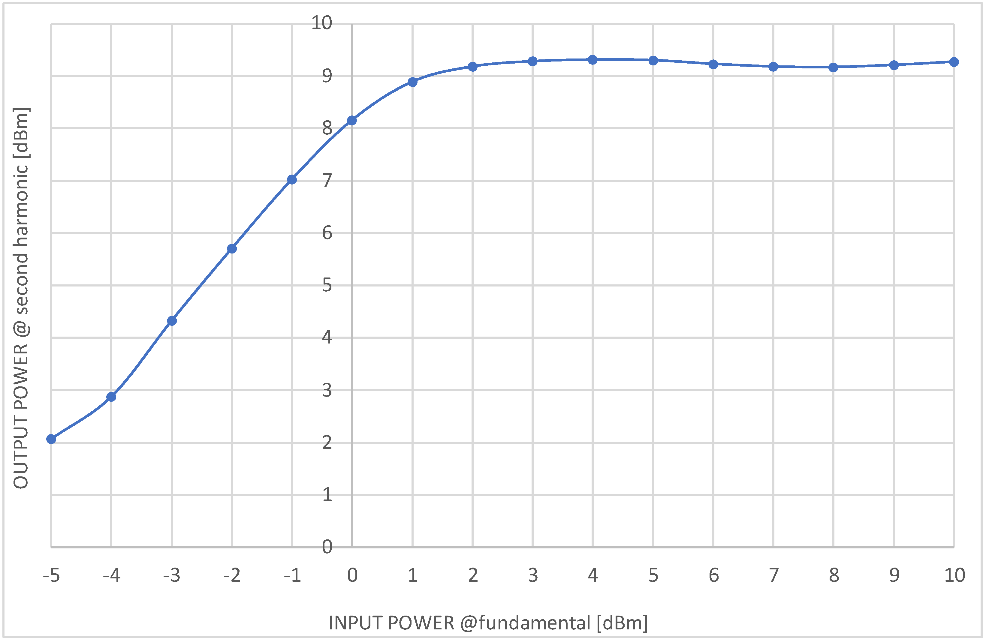
3. Results
4. Discussion
5. Conclusions
Author Contributions
Funding
Institutional Review Board Statement
Informed Consent Statement
Data Availability Statement
Conflicts of Interest
References
- Maas, S.A. Nonlinear Microwave and RF Circuits, 2nd ed.; Artech House: Boston, MA, USA; London, UK, 2003; ISBN 978-1-58053-484-0. [Google Scholar]
- Deng, S.; Gao, C.; Chen, S.; Sun, J.; Wu, K. Research on Linearity Improvement of Silicon-Based p-i-n Diode Limiters. IEEE Microw. Wirel. Compon. Lett. 2020, 30, 62–65. [Google Scholar] [CrossRef]
- Echchakhaoui, K.; Abdelmounim, E.; Zbitou, J.; Bennis, H. New Design of Microwave Power Limiter. In Proceedings of the 2019 International Conference on Wireless Technologies, Embedded and Intelligent Systems (WITS), Fez, Morocco, 3–4 April 2019; IEEE: New York, NY, USA; pp. 1–3. [Google Scholar]
- Gauvin, J.; Vendier, O.; Cazaux, J.-L.; Blondy, P. Microwave Power Limiters Based on RF-MEMS. In Proceedings of the 2013 IEEE 26th International Conference on Micro Electro Mechanical Systems (MEMS), Taipei, Taiwan, 20–24 January 2013; IEEE: New York, NY, USA; pp. 769–772. [Google Scholar]
- Chaturvedi, S.; Saravanan, G.S.; Bhat, K.M.; Bhalke, S. MESFET Process Based Planar Schottky Diode and Its Application to Passive Power Limiters. In Proceedings of the IEEE MTT-S International Microwave and RF Conference, New Delhi, India, 14–16 December 2013; IEEE: New York, NY, USA; pp. 1–4. [Google Scholar]
- Lim, C.-L. Limiting and Transient Performances of a Low Loss PIN-Schottky Limiter. In Proceedings of the 2013 IEEE International RF and Microwave Conference (RFM), Penang, Malaysia, 9–11 December 2013; IEEE: New York, NY, USA; pp. 6–10. [Google Scholar]
- Wang, D.; Gao, L.; Zheng, S.; Deng, F.; Hou, D. Investigation on the Pulse Characteristics of RF/Microwave Limiter Based on Multistage PIN Diodes and Schottky Diodes. In Proceedings of the Proceedings of the 2014 3rd Asia-Pacific Conference on Antennas and Propagation, Harbin, China, 26–29 July 2014; IEEE: New York, NY, USA; pp. 1366–1369. [Google Scholar]
- Luo, R.; Bai, X.; Diao, S.; Lin, F. A 1mW CMOS Limiting Amplifier and RSSI for ZigBee—Applications. In Proceedings of the 2013 IEEE International Wireless Symposium (IWS), Beijing, China, 14–18 April 2013; IEEE: New York, NY, USA; pp. 1–4. [Google Scholar]
- Wang, D.; Gao, L.; Zheng, S. Design and Experimental Verification of Active RF Front-End Limiter with High Isolation Degree and Nanoseconds Response Time. In Proceedings of the 2015 IEEE 6th International Symposium on Microwave, Antenna, Propagation, and EMC Technologies (MAPE), Shanghai, China, 28–30 October 2015; IEEE: New York, NY, USA; pp. 534–538. [Google Scholar]
- Echchakhaoui, K.; Abdelmounim, E.H.; Zbitou, J.; Tajmouati, A.; Bennis, H.; Angel, M. An Evolved Design of a Zero Bias Broadband Microstrip Power Limiter. In Proceedings of the 2017 International Conference on Wireless Technologies, Embedded and Intelligent Systems (WITS), Fez, Morocco, 19–20 April 2017; IEEE: New York, NY, USA; pp. 1–4. [Google Scholar]
- Maas, A.P.M.; Janssen, J.P.B.; van Vliet, F.E. Set of X-Band Distributed Absorptive Limiter GaAs MMICs. In Proceedings of the 2007 European Radar Conference, Munich, Germany, 10–12 October 2007; IEEE: New York, NY, USA; pp. 17–20. [Google Scholar]
- Nam, S.; Traut, F.; Cuggino, J. A Ka-Band High Power Frequency Doubler in SMT Package. In Proceedings of the 2006 IEEE Compound Semiconductor Integrated Circuit Symposium, San Antonio, TX, USA, 12–15 November 2006; IEEE: New York, NY, USA; pp. 61–64. [Google Scholar]
- Cseppento, B.; Berceli, T.; Nagy, A.; Billabert, A.-L. A Multiplier-Type Microwave FET Mixer. In Proceedings of the 2017 Mediterranean Microwave Symposium (MMS), Marseille, France, 28–30 November 2017; IEEE: New York, NY, USA; pp. 1–5. [Google Scholar]
- Jonsson, M.; Zirath, H.; Yhland, K. A New FET Frequency Multiplier. In Proceedings of the 1998 IEEE MTT-S International Microwave Symposium Digest (Cat. No.98CH36192), Baltimore, MD, USA, 7–12 June 1998; IEEE: New York, NY, USA; Volume 3, pp. 1427–1430. [Google Scholar]
- Yuk, K.; Branner, G.R.; Wong, C. High Power, High Conversion Gain Frequency Doublers Using SiC MESFETs and AlGaN/GaN HEMTs. In Proceedings of the 2010 IEEE MTT-S International Microwave Symposium, Anaheim, CA, USA, 23–28 May 2010; IEEE: New York, NY, USA; pp. 1008–1011. [Google Scholar]
- Zomorrodian, V.; York, R.A. A MMIC Frequency Doubler Using AlGaN/GaN HEMT Technology. In Proceedings of the 2011 IEEE Compound Semiconductor Integrated Circuit Symposium (CSICS), Waikoloa, HI, USA, 14–17 October 2011; IEEE: New York, NY, USA; pp. 1–4. [Google Scholar]
- Werthof, A.; Tischer, H.; Grave, T. High Gain PHEMT Frequency Doubler for 76 GHz Automotive Radar. In Proceedings of the 2001 IEEE MTT-S International Microwave Sympsoium Digest (Cat. No.01CH37157), Phoenix, AZ, USA, 20–24 May 2001; IEEE: New York, NY, USA; Volume 1, pp. 107–109. [Google Scholar]
- Nallandhigal, S.N.; Lu, Y.; Wu, K. Unified Integration Space of Multi-FET Active Frequency Multiplier and Multiport Antenna. IEEE Microw. Wirel. Compon. Lett. 2020, 30, 429–432. [Google Scholar] [CrossRef]
- Biswas, B.; Kumar, G.A. A Power Efficient Ka-Band MMIC Active Frequency Doubler with Output Amplifier. In Proceedings of the 2017 IEEE MTT-S International Microwave and RF Conference (IMaRC), Ahmedabad, India, 11–13 December 2017; IEEE: New York, NY, USA; pp. 1–5. [Google Scholar]
- Chang, H.-Y.; Chen, G.-Y.; Hsin, Y.-M. A Broadband High Efficiency High Output Power Frequency Doubler. IEEE Microw. Wirel. Compon. Lett. 2010, 20, 226–228. [Google Scholar] [CrossRef]
- Tang, W.; Tang, S.; He, Q.; Shao, Z. High Conversion Gain Broadband Frequency Doubler Design. In Proceedings of the 2010 International Conference on Microwave and Millimeter Wave Technology, Chengdu, China, 8–11 May 2010; IEEE: New York, NY, USA; pp. 536–538. [Google Scholar]
- Jun, L.; Weihua, Y.; Yanfei, H.; Xudong, W.; Haidong, Q.; Xin, L. D Band Active Integrated Frequency Doubler MMIC Based on InP HEMT Technology. In Proceedings of the 2018 International Conference on Microwave and Millimeter Wave Technology (ICMMT), Chengdu, China, 7–11 May 2018; IEEE: New York, NY, USA; pp. 1–3. [Google Scholar]
- Weiss, M.D.; Popovic, Z. An X/K-Band Class-E High-Efficiency Frequency Doubler. In Proceedings of the 31st European Microwave Conference, London, UK, 24–26 September 2001; IEEE: New York, NY, USA, 2001; pp. 1–4. [Google Scholar]
- Yamauchi, K.; Mori, K.; Nakayama, M.; Mitsui, Y.; Takagi, T. A Microwave Miniaturized Linearizer Using a Parallel Diode with a Bias Feed Resistance. IEEE Trans. Microw. Theory Tech. 1997, 45, 2431–2435. [Google Scholar] [CrossRef]
- Camargo, E. Design of FET Frequency Multipliers and Harmonic Oscillators; Artech House: Boston, MA, USA; London, UK, 1998; ISBN 978-0-89006-481-8. [Google Scholar]


| Pin (dBm) | Pout (dBm) |
|---|---|
| −20 | −29.29 |
| −14 | −16.92 |
| −10 | −7.52 |
| −5 | 2.07 |
| −4 | 2.88 |
| −3 | 4.33 |
| −2 | 5.71 |
| −1 | 7.03 |
| 0 | 8.16 |
| 1 | 8.89 |
| 2 | 9.18 |
| 3 | 9.28 |
| 4 | 9.31 |
| 5 | 9.30 |
| 6 | 9.23 |
| 7 | 9.18 |
| 8 | 9.17 |
| 9 | 9.21 |
| 10 | 9.27 |
Disclaimer/Publisher’s Note: The statements, opinions and data contained in all publications are solely those of the individual author(s) and contributor(s) and not of MDPI and/or the editor(s). MDPI and/or the editor(s) disclaim responsibility for any injury to people or property resulting from any ideas, methods, instructions or products referred to in the content. |
© 2023 by the authors. Licensee MDPI, Basel, Switzerland. This article is an open access article distributed under the terms and conditions of the Creative Commons Attribution (CC BY) license (https://creativecommons.org/licenses/by/4.0/).
Share and Cite
Kwiatkowski, P.; Knioła, M.; Szczepaniak, Z. Microwave Frequency Doubler with Improved Stabilization of Output Power. Sensors 2023, 23, 3598. https://doi.org/10.3390/s23073598
Kwiatkowski P, Knioła M, Szczepaniak Z. Microwave Frequency Doubler with Improved Stabilization of Output Power. Sensors. 2023; 23(7):3598. https://doi.org/10.3390/s23073598
Chicago/Turabian StyleKwiatkowski, Piotr, Michał Knioła, and Zenon Szczepaniak. 2023. "Microwave Frequency Doubler with Improved Stabilization of Output Power" Sensors 23, no. 7: 3598. https://doi.org/10.3390/s23073598
APA StyleKwiatkowski, P., Knioła, M., & Szczepaniak, Z. (2023). Microwave Frequency Doubler with Improved Stabilization of Output Power. Sensors, 23(7), 3598. https://doi.org/10.3390/s23073598