Analysis of Training Deep Learning Models for PCB Defect Detection
Abstract
1. Introduction
2. Related Work
3. Properties of PCB Images
3.1. Public PCB Datasets
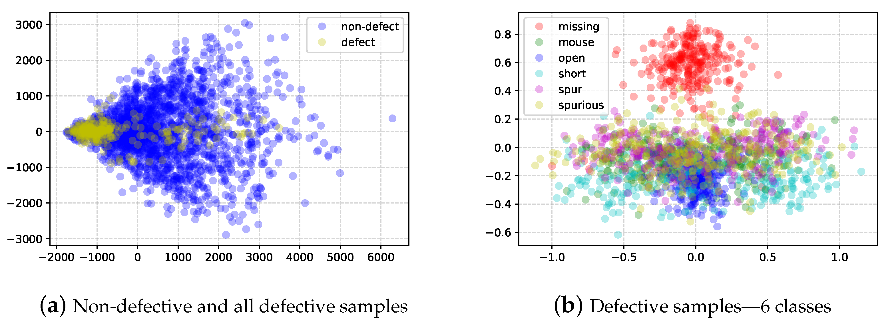
3.2. Attributes of Industrial Data
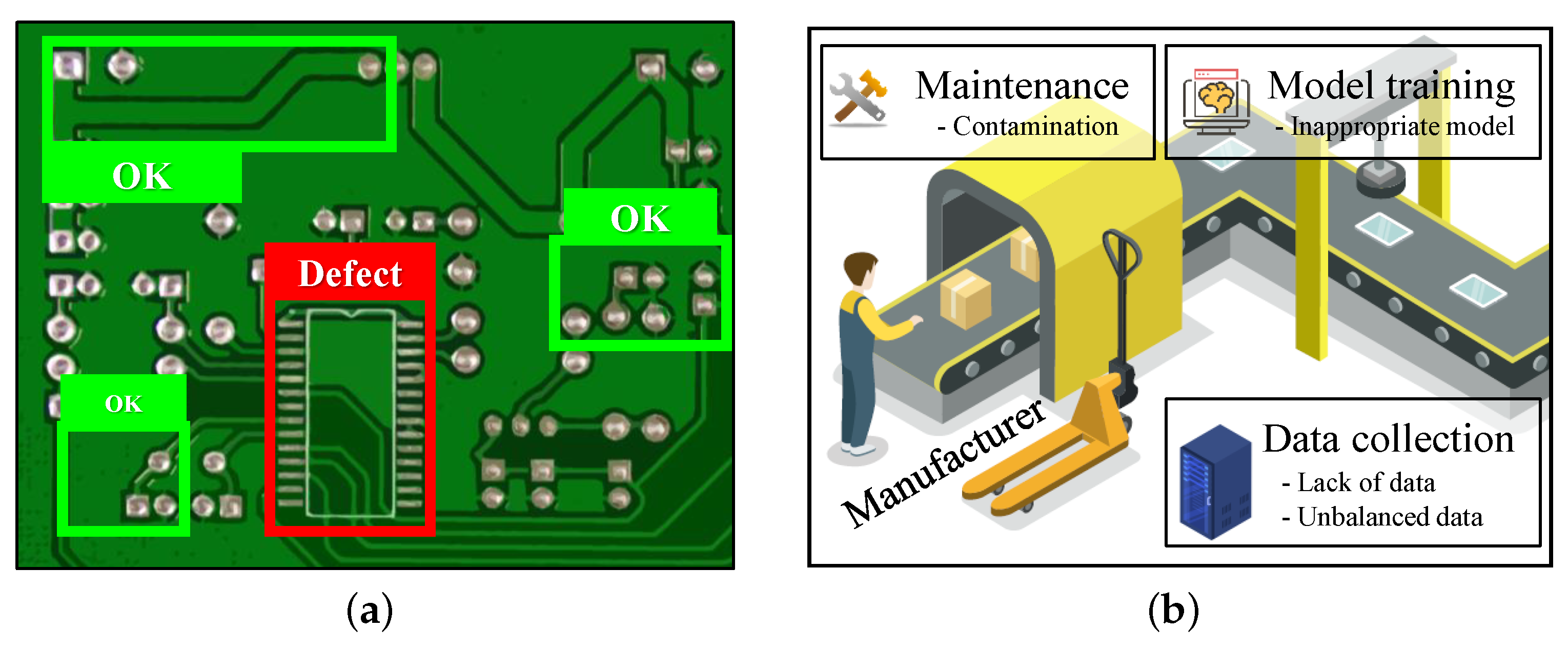
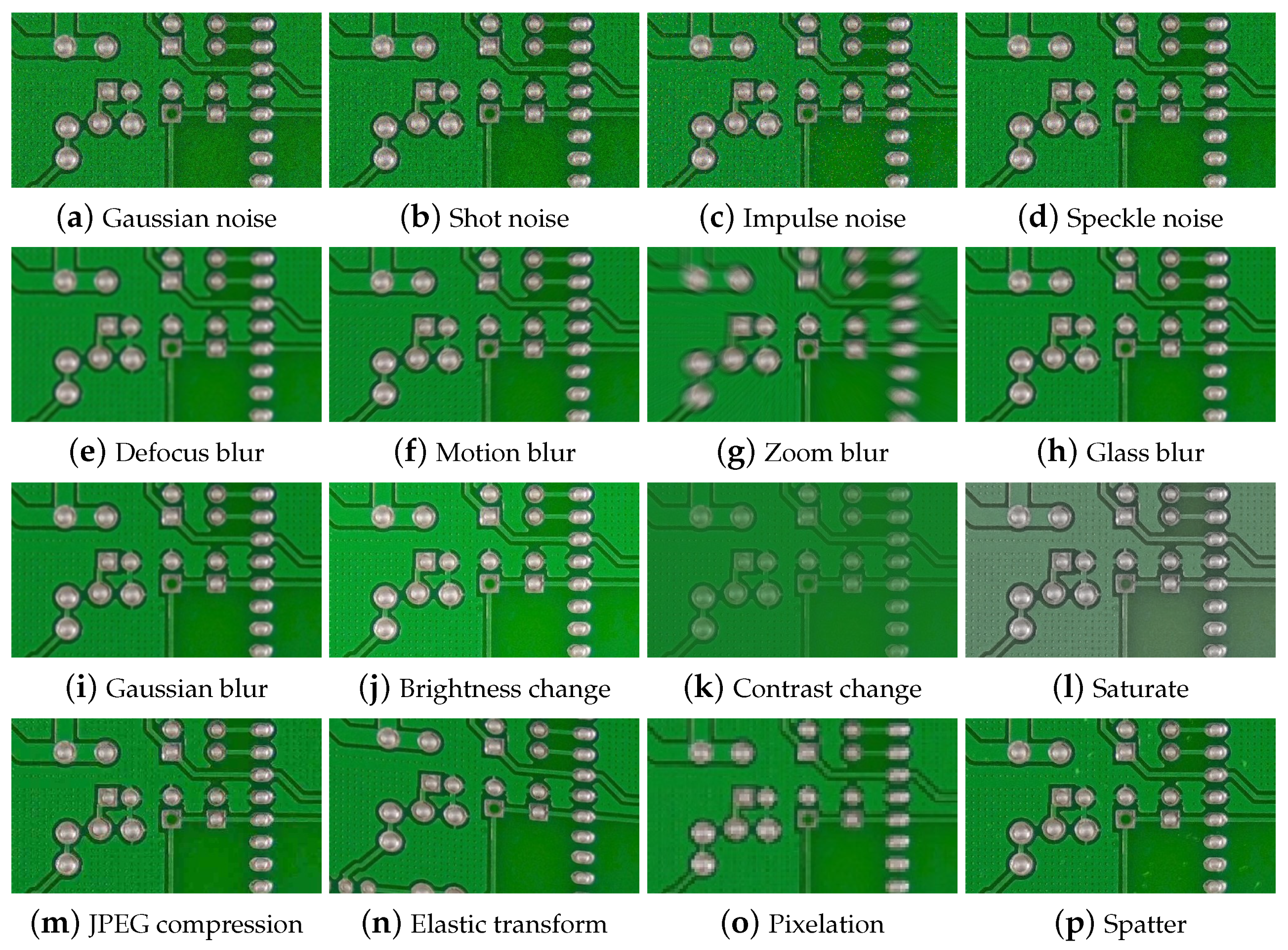
3.3. Image Contamination
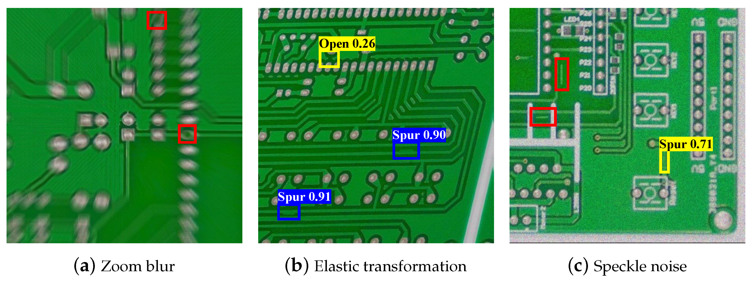
- Close-up imaging: Close-up imaging is required to inspect small electronic parts in detail. However, a small vibration of the camera or product causes significant blurring and image degradation. For example, subtle changes in intrinsic camera parameters occur, such as defocus and zoom blurring. In addition, subtle camera pose changes or PCB movements occur, such as elastic transforms and motion blur.
- Illumination changes: Generally, manufacturing equipment blocks external light and uses internal lighting to avoid the influence of external light sources. The quality of the image changes sensitively depending on the lighting condition. According to the lighting variation, images are affected by noise (e.g., Gaussian and impulse) and color variations (e.g., brightness change, contrast change, and saturation).
- Long-term maintenance: During long-term manufacturing, various image degradation factors, such as dirt on the lens and PCB, dust and steam particles in the air, and others, occur, which can cause glass blur and spatter contamination.
- Systematic issues: Factory facilities require enough storage, but some older factories may not be equipped with enough storage capacity to handle the generation of vast amounts of image data. For example, multiple high-resolution images (e.g., 4 K image) are taken for each product and thousands of products are produced per day, a single production line can easily generate about 1 TB of data each week. Managing large-scale images while the factory is in operation is a challenging task. Therefore, image compression is necessary within the industrial field. A lossy image compression can be an effective solution to reduce image capacity, but the image quality degrades. In this case, JPEG compression and pixelation can occur.
4. Methods of PCB Defect Detection
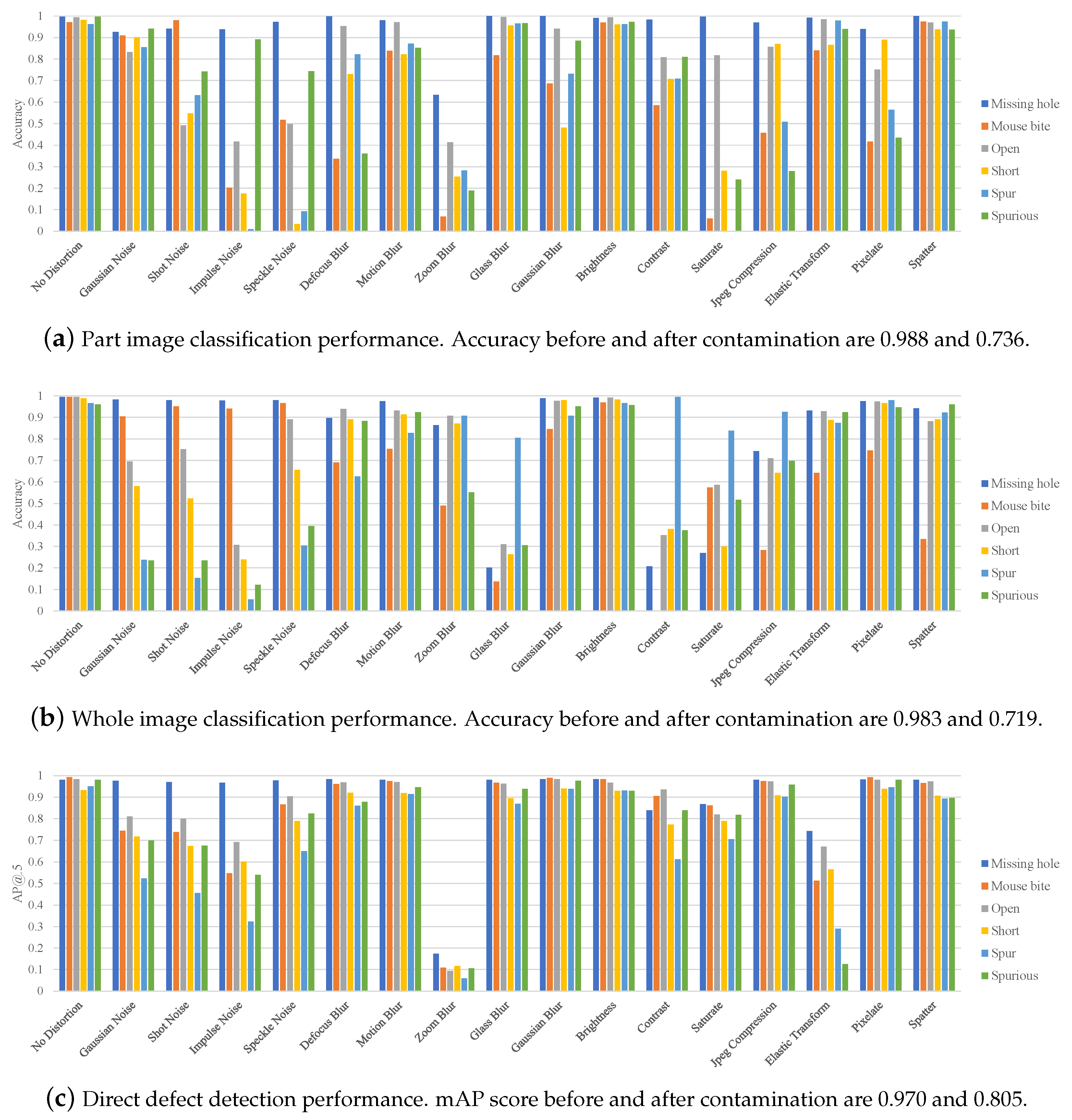
- Part image classification is a method that distinguishes classes of input images. It takes cropped image patches as model input and predicts the class of input cropped data. The prediction results include the class of electronic component images and whether they are defective. We can apply image classification when the location and size of each electronic part are known. This method focuses on classifying the electronic parts at a specified location.
- Whole image understanding examines whole PCB images and determines whether parts or circuits in the image are defective. Training for image understanding does not require the specified location of each part but only the images and their labels, so the training data collection is simple. This method is suitable to employ where the locations of defects at the PCB are not specified. It does not directly infer the location and size of the defective part but only determines whether the whole PCB image contains defective parts. Therefore, we must implement an additional algorithm, such as the class activation map (CAM) [38], to visualize predictions of the image understanding model.
- Direct defect detection receives the whole PCB image as input and predicts the location, size, and class of the defects. The PCB images and annotations on the location, size, and type of the defects are necessary to learn the defect detection model. If the defect can occur at an unspecified location rather than a specified location in the image, applying the defect detection method is advantageous.
5. Experiments
5.1. Settings
5.2. Defect Detection Performance According to Training Data Volume
5.3. Defect Detection Performance According to Possible Contamination
6. Discussion on PCB Defect Detection
7. Conclusions and Future Works
Author Contributions
Funding
Institutional Review Board Statement
Informed Consent Statement
Data Availability Statement
Conflicts of Interest
References
- Cucchiella, F.; D’Adamo, I.; Rosa, P.; Terzi, S. Automotive printed circuit boards recycling: An economic analysis. J. Clean. Prod. 2016, 121, 130–141. [Google Scholar] [CrossRef]
- Malge, P.; Nadaf, R. PCB defect detection, classification and localization using mathematical morphology and image processing tools. Int. J. Comput. Appl. 2014, 87, 40–45. [Google Scholar]
- Moganti, M.; Ercal, F.; Dagli, C.H.; Tsunekawa, S. Automatic PCB inspection algorithms: A survey. Comput. Vis. Image Underst. 1996, 63, 287–313. [Google Scholar] [CrossRef]
- Lee, J.H.; Oh, H.M.; Kim, M.Y. Deep learning based 3D defect detection system using photometric stereo illumination. In Proceedings of the 2019 International Conference on Artificial Intelligence in Information and Communication (ICAIIC), Okinawa, Japan, 11–13 February 2019; pp. 484–487. [Google Scholar]
- Malge, P.; Nadaf, R. A survey: Automated visual pcb inspection algorithm. Int. J. Eng. Res. Technol. (IJERT) 2014, 3, 223–229. [Google Scholar]
- Putera, S.I.; Ibrahim, Z. Printed circuit board defect detection using mathematical morphology and MATLAB image processing tools. In Proceedings of the 2010 2nd International Conference on Education Technology and Computer, Shanghai, China, 22–24 June 2010; Volume 5, p. V5-359. [Google Scholar]
- Chang, P.C.; Chen, L.Y.; Fan, C.Y. A case-based evolutionary model for defect classification of printed circuit board images. J. Intell. Manuf. 2008, 19, 203–214. [Google Scholar] [CrossRef]
- Wei, P.; Liu, C.; Liu, M.; Gao, Y.; Liu, H. CNN-based reference comparison method for classifying bare PCB defects. J. Eng. 2018, 2018, 1528–1533. [Google Scholar] [CrossRef]
- Abd Al Rahman, M.; Mousavi, A. A review and analysis of automatic optical inspection and quality monitoring methods in electronics industry. IEEE Access 2020, 8, 183192–183271. [Google Scholar]
- Chen, J.; Ran, X. Deep learning with edge computing: A review. Proc. IEEE 2019, 107, 1655–1674. [Google Scholar] [CrossRef]
- Huang, R.; Gu, J.; Sun, X.; Hou, Y.; Uddin, S. A rapid recognition method for electronic components based on the improved YOLO-V3 network. Electronics 2019, 8, 825. [Google Scholar] [CrossRef]
- Johnson, J.M.; Khoshgoftaar, T.M. Survey on deep learning with class imbalance. J. Big Data 2019, 6, 1–54. [Google Scholar] [CrossRef]
- Deng, J.; Dong, W.; Socher, R.; Li, L.J.; Li, K.; Fei-Fei, L. Imagenet: A large-scale hierarchical image database. In Proceedings of the 2009 IEEE Conference on Computer Vision and Pattern Recognition, Miami, FL, USA, 20–25 June 2009; pp. 248–255. [Google Scholar]
- Lin, T.Y.; Maire, M.; Belongie, S.; Hays, J.; Perona, P.; Ramanan, D.; Dollár, P.; Zitnick, C.L. Microsoft coco: Common objects in context. In Proceedings of the Computer Vision—ECCV 2014: 13th European Conference, Zurich, Switzerland, 6–12 September 2014; Springer: Berlin/Heidelberg, Germany, 2014; pp. 740–755. [Google Scholar]
- Kim, J.; Ko, J.; Choi, H.; Kim, H. Printed circuit board defect detection using deep learning via a skip-connected convolutional autoencoder. Sensors 2021, 21, 4968. [Google Scholar] [CrossRef]
- Liao, X.; Lv, S.; Li, D.; Luo, Y.; Zhu, Z.; Jiang, C. YOLOv4-MN3 for PCB Surface Defect Detection. Appl. Sci. 2021, 11, 11701. [Google Scholar] [CrossRef]
- Ojala, T.; Pietikäinen, M.; Harwood, D. A comparative study of texture measures with classification based on featured distributions. Pattern Recognit. 1996, 29, 51–59. [Google Scholar] [CrossRef]
- Dalal, N.; Triggs, B. Histograms of oriented gradients for human detection. In Proceedings of the 2005 IEEE Computer Society Conference on Computer Vision and Pattern Recognition (CVPR’05), San Diego, CA, USA, 20–26 June 2005; Volume 1, pp. 886–893. [Google Scholar]
- Ho, T.K. Random decision forests. In Proceedings of the 3rd International Conference on Document Analysis and Recognition, Montreal, QC, Canada, 14–16 August 1995; Volume 1, pp. 278–282. [Google Scholar]
- Hearst, M.A.; Dumais, S.T.; Osuna, E.; Platt, J.; Scholkopf, B. Support vector machines. IEEE Intell. Syst. Their Appl. 1998, 13, 18–28. [Google Scholar] [CrossRef]
- LeCun, Y.; Jackel, L.; Bottou, L.; Brunot, A.; Cortes, C.; Denker, J.; Drucker, H.; Guyon, I.; Muller, U.; Sackinger, E.; et al. Comparison of learning algorithms for handwritten digit recognition. In Proceedings of the International Conference on Artificial Neural Networks, Perth, Australia, 27 November–1 December 1995; Volume 60, pp. 53–60. [Google Scholar]
- Szegedy, C.; Liu, W.; Jia, Y.; Sermanet, P.; Reed, S.; Anguelov, D.; Erhan, D.; Vanhoucke, V.; Rabinovich, A. Going deeper with convolutions. In Proceedings of the the IEEE Conference on Computer Vision and Pattern Recognition, Boston, MA, USA, 7–12 June 2015; pp. 1–9. [Google Scholar]
- Dave, N.; Tambade, V.; Pandhare, B.; Saurav, S. PCB defect detection using image processing and embedded system. Int. Res. J. Eng. Technol. (IRJET) 2016, 3, 1897–1901. [Google Scholar]
- Malaca, P.; Rocha, L.F.; Gomes, D.; Silva, J.; Veiga, G. Online inspection system based on machine learning techniques: Real case study of fabric textures classification for the automotive industry. J. Intell. Manuf. 2019, 30, 351–361. [Google Scholar] [CrossRef]
- Takada, Y.; Shiina, T.; Usami, H.; Iwahori, Y.; Bhuyan, M. Defect detection and classification of electronic circuit boards using keypoint extraction and CNN features. In Proceedings of the Ninth International Conferences on Pervasive Patterns and Applications Defect, Athens, Greece, 19–23 February 2017; Volume 100, pp. 113–116. [Google Scholar]
- Ren, R.; Hung, T.; Tan, K.C. A generic deep-learning-based approach for automated surface inspection. IEEE Trans. Cybern. 2017, 48, 929–940. [Google Scholar] [CrossRef]
- Adibhatla, V.A.; Chih, H.C.; Hsu, C.C.; Cheng, J.; Abbod, M.F.; Shieh, J.S. Applying deep learning to defect detection in printed circuit boards via a newest model of you-only-look-once. Math. Biosci. Eng. 2021, 18, 4411–4428. [Google Scholar] [CrossRef]
- Lian, J.; Wang, L.; Liu, T.; Ding, X.; Yu, Z. Automatic visual inspection for printed circuit board via novel Mask R-CNN in smart city applications. Sustain. Energy Technol. Assess. 2021, 44, 101032. [Google Scholar] [CrossRef]
- Huang, W.; Wei, P. A PCB dataset for defects detection and classification. arXiv 2019, arXiv:1901.08204. [Google Scholar]
- Ding, R.; Dai, L.; Li, G.; Liu, H. TDD-net: A tiny defect detection network for printed circuit boards. CAAI Trans. Intell. Technol. 2019, 4, 110–116. [Google Scholar] [CrossRef]
- Lu, H.; Mehta, D.; Paradis, O.; Asadizanjani, N.; Tehranipoor, M.; Woodard, D.L. Fics-pcb: A multi-modal image dataset for automated printed circuit board visual inspection. Cryptol. ePrint Arch. 2020. Available online: https://eprint.iacr.org/2020/366 (accessed on 1 February 2023).
- Pramerdorfer, C.; Kampel, M. A dataset for computer-vision-based PCB analysis. In Proceedings of the 2015 14th IAPR International Conference on Machine Vision Applications (MVA), Tokyo, Japan, 18–22 May 2015; pp. 378–381. [Google Scholar]
- Mahalingam, G.; Gay, K.M.; Ricanek, K. Pcb-metal: A pcb image dataset for advanced computer vision machine learning component analysis. In Proceedings of the 2019 16th International Conference on Machine Vision Applications (MVA), Tokyo, Japan, 27–31 May 2019; pp. 1–5. [Google Scholar]
- Liu, T.; Bao, J.; Wang, J.; Wang, J. Deep learning for industrial image: Challenges, methods for enriching the sample space and restricting the hypothesis space, and possible issue. Int. J. Comput. Integr. Manuf. 2021, 35, 1077–1106. [Google Scholar] [CrossRef]
- Hendrycks, D.; Dietterich, T. Benchmarking neural network robustness to common corruptions and perturbations. arXiv 2019, arXiv:1903.12261. [Google Scholar]
- Huang, S.; Papernot, N.; Goodfellow, I.; Duan, Y.; Abbeel, P. Adversarial attacks on neural network policies. arXiv 2017, arXiv:1702.02284. [Google Scholar]
- Bergmann, P.; Fauser, M.; Sattlegger, D.; Steger, C. MVTec AD—A Comprehensive Real-World Dataset for Unsupervised Anomaly Detection. In Proceedings of the the IEEE/CVF Conference on Computer Vision and Pattern Recognition (CVPR), Long Beach, CA, USA, 15–20 June 2019. [Google Scholar]
- Selvaraju, R.R.; Cogswell, M.; Das, A.; Vedantam, R.; Parikh, D.; Batra, D. Grad-cam: Visual explanations from deep networks via gradient-based localization. In Proceedings of the the IEEE International Conference on Computer Vision, Venice, Italy, 22–29 October 2017; pp. 618–626. [Google Scholar]
- Wu, W.Y.; Wang, M.J.J.; Liu, C.M. Automated inspection of printed circuit boards through machine vision. Comput. Ind. 1996, 28, 103–111. [Google Scholar] [CrossRef]
- Kaur, B.; Kaur, G.; Kaur, A. Detection and classification of printed circuit board defects using image subtraction method. In Proceedings of the 2014 Recent Advances in Engineering and Computational Sciences (RAECS), Chandigarh, India, 6–8 March 2014; pp. 1–5. [Google Scholar]
- He, K.; Zhang, X.; Ren, S.; Sun, J. Deep residual learning for image recognition. In Proceedings of the the IEEE Conference on Computer Vision and Pattern Recognition, Las Vegas, NV, USA, 26 June–1 July 2016; pp. 770–778. [Google Scholar]
- Wang, C.Y.; Bochkovskiy, A.; Liao, H.Y.M. YOLOv7: Trainable bag-of-freebies sets new state-of-the-art for real-time object detectors. arXiv 2022, arXiv:2207.02696. [Google Scholar]
- Jones, C.T. Programmable Logic Controllers: The Complete Guide to the Technology; Brilliant-Training: Kepulauan Riau, Indonesia, 1998. [Google Scholar]
- Saenz de Ugarte, B.; Artiba, A.; Pellerin, R. Manufacturing execution system–a literature review. Prod. Plan. Control 2009, 20, 525–539. [Google Scholar] [CrossRef]


| Dataset | Images | Cropped Images | Types of Defects | # of Defects | Types of Positives |
|---|---|---|---|---|---|
| PCB [29] | 10 | 690 |  | 2070 | Any circuits or parts except for defects |
| TDD-PCB [30] | 10 | 10,668 | 21,336 | ||
| FICS-PCB [31] | 31 | 400 | None | None | IC Chip (3243) Capacitors (36,639) Resistors (33,182) Inductors (1292) Transistors (1398) Diodes (1593) |
| PCB DSLR [32] | 165 | 849 | None | None | IC Chip (9313) |
| PCB-METAL [33] | 123 | 984 | None | None | IC Chip (5844) Capacitors (3175) Resistors (2670) Inductors (542) |
| Attribute | Descriptions |
|---|---|
| Small amount |
|
| Small object |
|
| Imbalance |
|
| Fine-grained |
|
| Strong interference |
|
| Temporality |
|
| Factor | Possible Contamination |
|---|---|
| Close-up imaging | • Defocus blur, Motion blur, Zoom blur, Gaussian blur • Elastic transform |
| Illumination changes | • Gaussian noise, Shot noise, Impulse noise, Speckle noise • Brightness • Contrast change • Saturate |
| Long-term maintenance | • Glass blur • Spatter |
| Systematic issues | • JPEG compression • Pixelation |
| Part Image Classification | Whole Image Understanding | Direct Defect Detection | |
|---|---|---|---|
| Training data |
|
|
|
| Test data | Cropped part image | PCB image | PCB image |
| Model prediction | Class of the part image | Class of PCB image | Defect location and class |
| Result examples | 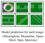 | 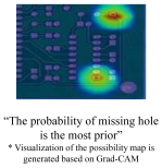 |  |
| Accuracy of Part Image Classification (Model: ResNet50 [41]) | ||||||||
| Data Ratio | Missinghole | Mousebite | Open | Short | Spur | Spurious | Non-Defective | Avg. |
| 80/20 | 0.996 | 0.972 | 0.993 | 0.982 | 0.962 | 0.997 | 0.998 | 0.988 |
| 50/50 | 0.962 | 0.980 | 0.994 | 0.988 | 0.969 | 0.999 | 0.961 | 0.975 |
| 20/80 | 0.997 | 0.983 | 0.980 | 0.972 | 0.976 | 0.963 | 0.964 | 0.974 |
| 10/90 | 0.988 | 0.972 | 0.979 | 0.928 | 0.962 | 0.962 | 0.995 | 0.975 |
| 5/95 | 0.979 | 0.980 | 0.966 | 0.940 | 0.932 | 0.967 | 0.983 | 0.968 |
| Accuracy of Whole Image Understanding (Model: ResNet50 [41]) | ||||||||
| Data Ratio | Missinghole | Mousebite | Open | Short | Spur | Spurious | Non-Defective | Avg. |
| 80/20 | 0.994 | 0.994 | 0.994 | 0.988 | 0.965 | 0.960 | - | 0.983 |
| 50/50 | 0.991 | 0.493 | 0.379 | 0.789 | 0.285 | 0.241 | - | 0.532 |
| 20/80 | 0.989 | 0.258 | 0.192 | 0.222 | 0.205 | 0.233 | - | 0.354 |
| 10/90 | 0.970 | 0.159 | 0.229 | 0.237 | 0.262 | 0.190 | - | 0.344 |
| 5/95 | 0.411 | 0.191 | 0.135 | 0.167 | 0.242 | 0.088 | - | 0.207 |
| Mean Average Precision (mAP) of Direct Defect Detection (Model: YOLOv7 [42]) | ||||||||
| Data Ratio | Missinghole | Mousebite | Open | Short | Spur | Spurious | Non-Defective | Avg. |
| 80/20 | 0.981 | 0.992 | 0.984 | 0.933 | 0.950 | 0.981 | - | 0.970 |
| 50/50 | 0.990 | 0.977 | 0.979 | 0.890 | 0.942 | 0.973 | - | 0.958 |
| 20/80 | 0.972 | 0.916 | 0.927 | 0.867 | 0.834 | 0.917 | - | 0.906 |
| 10/90 | 0.980 | 0.935 | 0.930 | 0.871 | 0.859 | 0.935 | - | 0.918 |
| 5/95 | 0.976 | 0.912 | 0.874 | 0.830 | 0.777 | 0.852 | - | 0.870 |
Disclaimer/Publisher’s Note: The statements, opinions and data contained in all publications are solely those of the individual author(s) and contributor(s) and not of MDPI and/or the editor(s). MDPI and/or the editor(s) disclaim responsibility for any injury to people or property resulting from any ideas, methods, instructions or products referred to in the content. |
© 2023 by the authors. Licensee MDPI, Basel, Switzerland. This article is an open access article distributed under the terms and conditions of the Creative Commons Attribution (CC BY) license (https://creativecommons.org/licenses/by/4.0/).
Share and Cite
Park, J.-H.; Kim, Y.-S.; Seo, H.; Cho, Y.-J. Analysis of Training Deep Learning Models for PCB Defect Detection. Sensors 2023, 23, 2766. https://doi.org/10.3390/s23052766
Park J-H, Kim Y-S, Seo H, Cho Y-J. Analysis of Training Deep Learning Models for PCB Defect Detection. Sensors. 2023; 23(5):2766. https://doi.org/10.3390/s23052766
Chicago/Turabian StylePark, Joon-Hyung, Yeong-Seok Kim, Hwi Seo, and Yeong-Jun Cho. 2023. "Analysis of Training Deep Learning Models for PCB Defect Detection" Sensors 23, no. 5: 2766. https://doi.org/10.3390/s23052766
APA StylePark, J.-H., Kim, Y.-S., Seo, H., & Cho, Y.-J. (2023). Analysis of Training Deep Learning Models for PCB Defect Detection. Sensors, 23(5), 2766. https://doi.org/10.3390/s23052766


