Abstract
Continuous monitoring and treatment of various diseases with biomedical technologies and wearable electronics has become significantly important. The healthcare area is an important, evolving field that, among other things, requires electronic and micro-electromechanical technologies. Designed circuits and smart devices can lead to reduced hospitalization time and hospitals equipped with high-quality equipment. Some of these devices can also be implanted inside the body. Recently, various implanted electronic devices for monitoring and diagnosing diseases have been presented. These instruments require communication links through wireless technologies. In the transmitters of these devices, power amplifiers are the most important components and their performance plays important roles. This paper is devoted to collecting and providing a comprehensive review on the various designed implanted amplifiers for advanced biomedical applications. The reported amplifiers vary with respect to the class/type of amplifier, implemented CMOS technology, frequency band, output power, and the overall efficiency of the designs. The purpose of the authors is to provide a general view of the available solutions, and any researcher can obtain suitable circuit designs that can be selected for their problem by reading this survey.
1. Introduction
The need for the healthcare system is increasing, as factors such as life style, food habits, environmental schemes, etc., are altering and may be deteriorating. As a result, healthcare offices and hospitals are required to have advanced equipment to be able to handle the increasing number of requirements of patients [1]. The integrated circuit (IC) technology used within biomedical implants is growing exponentially [2,3,4]. From another perspective, Internet of Things (IoT) systems will be fruitful in emerging applications that are based on radio frequency (RF) designs. IoT systems include computer, Internet, and mobile communication technologies [5]. Low-power RF circuits can be employed in industrial, scientific, and medical (ISM) bands that are suitable for medical applications. Hence, high-performance designs in terms of noise, bandwidth, linearity, etc., are substantially required [6,7]. In the field of medical applications, there is also a growing body of research on the acquisition and decoding of physiological signals [8].
RF power amplifiers (PAs) are widely used in industry, medical imaging, fifth-generation telecommunication, mobile communication networks, biomedical applications, and so on [9,10]. In medical applications, they are one of the most important technologies. For example, electroencephalograms (EEG) have recently been used for brain recording, as it is less expensive and more safe in magnetic fields [11,12]. For illustrating the importance of these medical devices, consider the example of a particle accelerator typically used for cancer diagnosis and prediction of initial treatment. To have effective performance in particles in a cyclotron, it has been important to use RF amplifiers, namely vacuum tube-type and solid state-type amplifiers [13]. Due to the highly infectious nature of the COVID-19 situation, doctors and patients are interested in wireless communication links [14]. Hence, medical devices, especially implanted devices, are substantially required to provide a ‘contact-less’ situation and to improve the link between performance and reliability [15]. By developing technology, implanted devices can serve the lives of many patients and can be used for clinical treatments [16,17,18].
For biomedical applications, it is essential to focus on the roles of patients, doctors, and nurses as well as the suitable placement of implanted devices inside or outside of the body. Additionally, for the implanted devices, some of the various specifications that must be considered are linearity, bandwidth, data rate, consumed power, and so on. In order to reduce the thermal influence in these devices, the heat generation of the designs must be minimized in order reduce any influence on the physiological activities. Furthermore, the overall circuit must have low power consumption [19].
Due to the importance of amplifiers in biomedical devices, this survey is devoted to summarizing the various circuits and technologies used for designing amplifiers and their use in medical applications. The remainder of this paper is as follows. Section 2 presents the biomedical devices and their benefits from an engineering perspective. Section 3 provides the various up-to-date biomedical and implanted amplifier designs that are used for diagnosing disease and treating patients. Section 4 presents a general view of the designed biomedical amplifiers from their layouts through to their fabrication. Because the measurements of these devices are important, Section 5 presents some of the methods employed for testing and measuring these devices. Finally, Section 6 concludes this manuscript.
2. Biomedical Devices from an Engineering Perspective
Figure 1 presents the various body parts where the implanted devices can be installed inside the body. Some of them substitute parts of the body, while others are embedded within various human tissues such as skin, fat, muscle, skull, dura, csf, and brain [20]. To illustrate the importance of these medical devices, brain signal acquisition front-end designs that involve amplifiers were presented in [21] (see Figure 2).
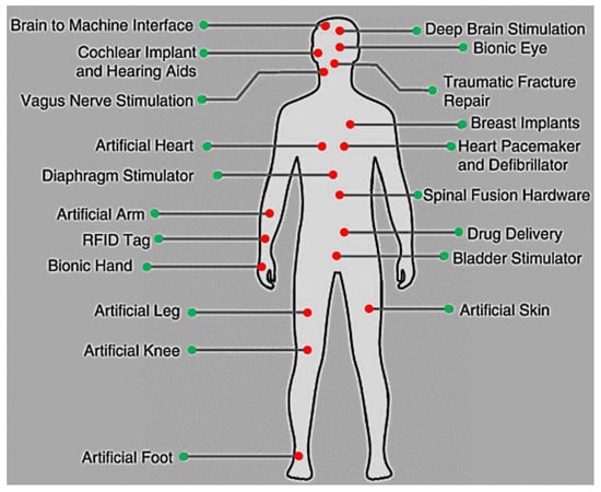
Figure 1.
Diverse body locations of implanted devices.
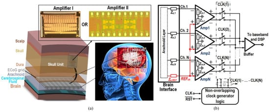
Figure 2.
(a) Structure of brain signal acquisition (BSA) front-ends, (b) low-noise amplifier presented in Reprinted/adapted with permission from Ref. [21]: Copyright 2023, IEEE.
For biomedical devices, the PA design is the essential element for transmitting/receiving RF signals, as presented in Figure 3. Overall, the transmitter is expected to achieve a suitable output power with the given efficiency. The PA structure is generally used for driving antennas and dissipates most of the power. Figure 4 presents the general procedure that antennae and amplifiers are provided for transferring data from patient to a medical doctor.
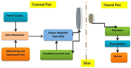
Figure 3.
Power amplifier and its importance in implanted devices [22].
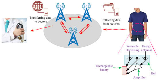
Figure 4.
Methodology for transferring data from patient to medical doctor [23].
Hence, the structure and output specifications of the PA play important roles [6].
CMOS-based transceivers (TRX) play an important role in biomedical applications [24,25], and they include both receiving and transmitting blocks as frequency synthesizers, voltage-controlled oscillators, amplifiers, and demodulators. For achieving high-performance TRX, each block must have good performance outcomes for generating and addressing high-magnitude pulses and modulations, respectively [6]. Recently, various methods devoted to the design of well-satisfied TRXs have been proposed, and some of the features exploited by researchers in the biomedical field are reported below.
3. Biomedical Amplifiers and Various Designs
The common and general bioelectric system includes the sensing, algorithm, and stimulation blocks [26]. Hence, designing and simulating each of these components requires special attention and multidisciplinary experience, as the chips are used for medical applications. This section provides a summary of various amplifiers used in medical applications using wireless technology.
Recording human electrocorticographic (ECoG) signals, especially for brain activity at a high resolution, suffers from a low signal-to-noise ratio and a low spatial resolution. In [27], an analog front-end (AFE) was presented that is appropriate for recording implants, and it includes a neural amplifier. The designed front-end amplifier provides a merged amplifier analog-to-digital converter (ADC) topology and wireless validation circuit. The architecture is employed in 65 nm CMOS technology with a consumed power of 3.2 μW with a common-mode rejection ratio (CMRR) of 77 dB. The layout of the AFE design includes a V/I converter, a current-controlled ring oscillator (ICRO)-based ADC, and a mixed-domain servo loop that is integrated into the recording system on a chip (SoC).
For the use of neural recording, an eight-channel AFE with a power supply rejection ratio (PSRR) of 110 dB and power supplies of 0.35 and 0.7 V was presented in [28]. Figure 5a presents the proposed amplifier for use in an interface SoC (see Figure 5b) where the maximum gain is 54 dB and the input-referred noise is 6.7 μV. The proposed replica biasing scheme provides suitable PSRR performance with stable bias current for the input stage of the low-noise amplifier (LNA). The consumed power is reduced using an averaged local field potential (A-LFP) servo loop where the signal is generated by integrating the four-channel programmable gain amplifier (PGA) outputs.
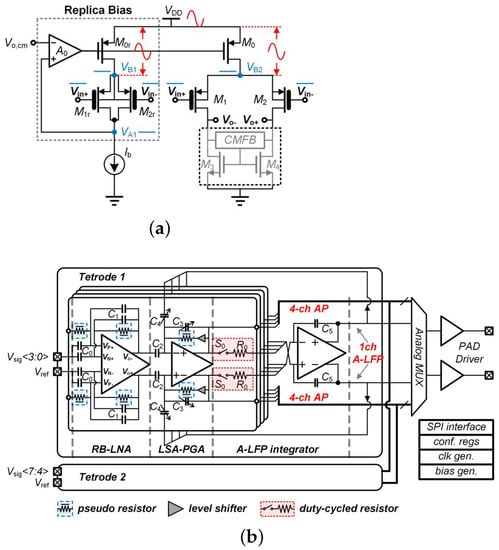
Figure 5.
(a) Presented amplifier including the replica biasing; (b) the implementation of amplifier in the presented neural interface SoC. Reprinted/adapted with permission from Ref. [28]: Copyright 2023, IEEE.
For treatment of several neural disorders, deep brain stimulation (DBS) was studied in [29] for a rat model using a battery-less mechanism in freely moving rats. The chip presented in that work is able to communicate with eight different brain regions, and the size of the chip was reduced. The microsystem performs transceiving actions through a single coil. The proposed chip includes a chopper-stabilized recording amplifier, an ADC, a multi-channel stimulation circuit, a programmable information hub, forward telemetry circuits, and reverse telemetry circuits. A detailed schematic of the chopper-stabilized LNA is presented in [29], and it adopts a fully differential architecture. The power per recording channel is 8.6 μW, with a stimulation frequency of 60 Hz to 220 Hz. The data rate for transmitter is 2 M bps and that of the receiver is 100 K bps.
Cruz et al. presented a low-intermediate frequency (IF) RF front-end that is appropriate for medical implant communication services [30]. It consists of an LNA and a mixer from 402 MHz to 405 MHz where the LNA achieves a 10 dB gain with a power consumption of 0.94 mW that is employed in the TSMC 0.18 m CMOS process. The presented circuit with the size of 1.4 mm × 1.2 mm (see more details in [30]) supports 446 kbps quadrature phase-shift keying (QPSK) modulation, which is a high data rate for a such design.
In various neuroscience experiments, neural amplifiers targeting deep brain regions play important roles for monitoring the disease. A high-power efficiency neural amplifier was presented in [31] with a minimum area of 0.051 mm that consumes 2.1 W using the 1 V supply, offering a DC input impedance of 6.7 G. In [31], a proposed neural amplifier was presented where no current flows from the input. In this design, due to the presence of a gain revision block, the buffer does not require charging of the input capacitor.
As described above, it is critical to have circuits with low power consumption and low complexity in biomedical applications. For wireless medical applications, on–off keying (OOK) design is used in [32] as a modulation/demodulation circuit for 2.4 GHz band with a power consumption of 160 W in the receiver and 0.6 W in the transmitter. The presented transceiver includes the receiver, which is subdivided into a input matching network, an LNA, a novel single-ton differential envelope detector, a level shifter, cascaded baseband amplifiers, and a hysteresis comparator. Additionally, the transmitter has a bias-stimulating circuit, a current-reuse self-mixing voltage controlled oscillator, and a quadruple-transconductance power amplifier. Due to the data rate of 20 Mbps and the energy efficiency of 80 pJ/bit, the overall transceiver is appropriate for implantable body sensor networks.
Ghanad et al. presented a local temperature monitoring system that is implantable, and it requires an the average power of 29.5 W [33]. The power dissipation of whole circuit can be decreased using a time-domain sensor readout and an OOK-modulated free-running oscillator. The implantable chip is designed and fabricated with 0.18 um CMOS technology where the sensor type is resistive with two channels. It has a sensitivity within ±220 . In [33], an implantable local temperature chip with 180 nm CMOS technology was presented. It includes various blocks for the implantable unit, and the temperature recording outcomes were tested inside the hot water. The brown adipose tissue (BAT) channel was employed for higher temperatures and normal body tissue was used for lower temperatures, where this channel recorded temperature above 39 °C.
A Class-E PA was presented in [34] for transferring power to medical implants using wideband frequency-shift keying (FSK) modulation with the carrier frequencies of 2 MHz and 4 MHz. The proposed PA can transmit data with a larger data rate to carrier frequency of 33%. As was previously mentioned, the carrier frequency of 2 MHz is twice that of the other carrier (i.e., 4 MHz), which results in wideband modulation and a power transfer efficiency (PTE) of 25%. The simplified PA is presented in [34], where it is able to transmit power with a data rate of 1 Mbps. In [35], another type of amplifier, a Class-D, was presented that works up to 14 MHz with an approximate efficiency of 80% and a maximum output power of 36 W. In [35], the general architecture of the Class-D PA is designed with 180 nm CMOS technology. It is an integrated PA with the ability to be used in wireless applications and medical transmitters.
In [36], a quad-shank CMOS neural probe was presented for the recording of multiple brain regions. For this case, the fully-differential channels are designed with an amplifier and a 14-bit ADC. For this design, no calibration is required and the total power consumption is 36.5 mW.
Hansen et al. presented a monolithic microwave wave integrated circuit (MMIC) where one of the blocks in the transmitter includes PA, and an LNA is used in the receiver [37]. This combination is a harmonic radar system that can be employed in the ISM frequency bands. The PA is employed here for sensing the transmitter signal and the LNA is used for enhancing the gain and sensitivity. The presented design can be used in the medical area where small reflectors need to be precisely determined.
In [38], a printed charge amplifier was presented for measuring on-skin biosignal. The design consists of organic transistors, and the used substrate is inkjet-printed Ag ink. The prepared measurement setup is presented in [38]. The circuit consists of integrated bias, feedback resistors, and a feedback capacitor that can be used for the evaluation of vascular health. The lower cut-off frequency can be varied by changing the value of the feedback resistor. Additionally, the arterial pulse wave signal is improved using the fully printed charge amplifier.
A fully-integrated low-power full-duplex transceiver (FDT) was presented in [39], where receiver and transmitter sections have one antenna, leading to a reduction in the complexity. The general structure of an implantable neural recording device is shown in Figure 6, which includes a 2.4 GHz on-chip receiver with binary phase-shift keying (BPSK) modulation, and TSMC 180 nm CMOS technology is used. The presented chip has a size of 0.8 m and provides an efficiency of 41.6% with a regulated power delivery of 25 mW.
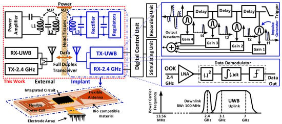
Figure 6.
The implantable neural recording device. Reprinted/adapted with permission from Ref. [39]: Copyright 2023, IEEE.
Using the 350 nm CMOS process, a trimodal neural interface system-on-chip (SoC) is explained in [40] that includes 16-channel neural recording. A conceptual view of the presented SoC is shown in Figure 7, which is installed on the head of a moving rat. In this chip, the stimulus artifact rejection injects a series of ±500 A into the model.
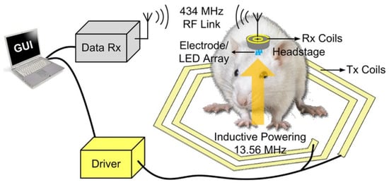
Figure 7.
Practical implementation of SoC on a rat. Reprinted/adapted with permission from Ref. [40]: Copyright 2023, IEEE.
In [41], a chronic implantable device simulated with 180 nm CMOS technology was presented. The general structure is presented in [41], and it includes various blocks such as amplifiers, oscillator, ADC blocks, and so on. This design is a ten-channel peripheral nerve electroneurogram (ENG), and it is validated in vivo for acquisition. Each amplifier channel within the chip is digitized with 10-bit resolution.
For implanted devices, the radio frequency identification (RFID) readers can receive the data, and provide suitable power. In [42], a structure for the RFID reader was presented where it included Class-E/Fodd PAs and incorporated a single-segmented antenna in the receiver and transmitter sections, which operate simultaneously. The typical efficiency of the design is 54%. The transceiver architecture is presented in [42], and the implementation of amplifiers is presented in detail in Figure 8.
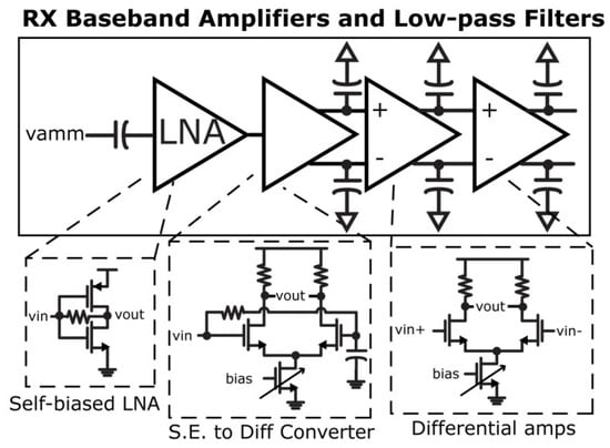
Figure 8.
Designed amplifiers with filters in [42]: Reprinted/adapted with permission. Copyright 2023, IEEE.
An integrated circuit to be used for medical implants is presented in [43], and the related structure includes three subsections (RF powering, transmitter, and signal acquisition) where the amplifier is placed in the transmitter block. The proposed structure includes a parallel-in/serial-out circuit (PISO), an injection-locked frequency divider (ILFD) for data transmission, a PA, and converters. These blocks are used for generating RF power, transmitting, and receiving data. The general structures of ILFD and PA are shown in [43]. The overall circuit generates a low-phase-noise carrier at 402 MHz.
Copani et al. presented a CMOS transceiver that can be used for low-power medical implants [44]. This implementation consists of a super-regenerative oscillator, an LNA, a class AB amplifier, and an injection-locked power oscillator. The general structure of the medical implant communication service (MICS) transceiver is depicted in [44]. Detailed structures of the super-regenerative wake-up oscillator (SRO), LNA, and PA are shown in Figure 9.
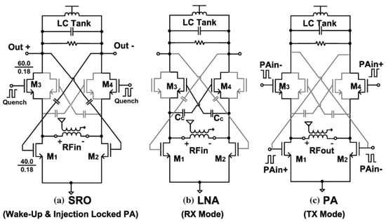
Figure 9.
Detailed structures of SRO, LNA, and PA designs for the MICS transceiver. Reprinted/adapted with permission from Ref. [44]: Copyright 2023, IEEE.
An arranged cloud health care network is presented in [45], where an antenna is employed for teeth implantation and an oscillator is connected to the antenna without any need for an amplifier. The used sampling amplifier with the antenna is presented in [45], where a practical implementation of the antenna in the mouth of patients results in a −6.78 dBi gain in performance. The overall structure presented in this study is able to monitor the temperature and transmit data wirelessly using cloud health care. The general structure of the healthcare-monitoring network is described in Figure 10.
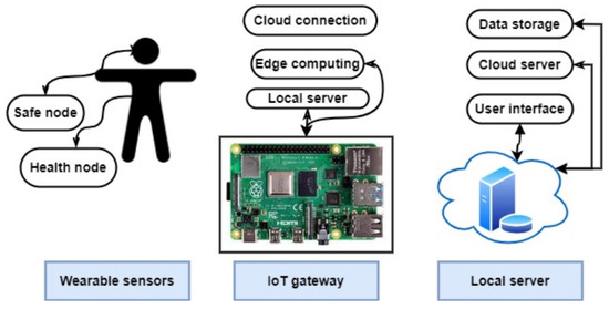
Figure 10.
Presented healthcare-monitoring network in [46].
In another study, a low-energy receiver using the LNA was reported that was designed in 65 nm CMOS technology [47]. This structure results in a noise figure of 8.2 dB and a gain of 49.5 dB.
In medical ultrasound imaging, endoscopic transducers are widely used and studied. A common problem related to this device is the lower signal-to-noise ratio in the image at high-frequency ultrasound waves. To tackle this problem, in [48] a high-sensitivity transducer with an integrated miniature amplifier was presented. The proposed amplifier can reduce the noise results and provide an enhanced potential for visualizing the deeper tissue of the human body. The general structure of the transducer with the micro-amplifier is presented in Figure 11. The achieved noise figure for the frequency band between 0 and 50 MHz demonstrates that the noise is sufficiently small and cannot affect the transducer waveform.
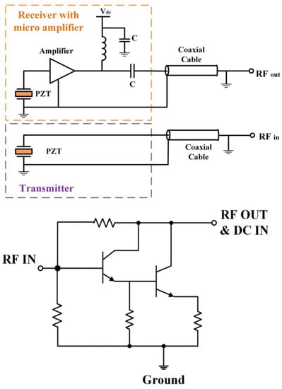
Figure 11.
The general structure of proposed transducer (top) with configuration of proposed amplifier (bottom) [48].
In [25], a brain–computer interface that can be substituted in the ear of human body with reduced noise was presented. The general structure is presented in Figure 12. The presented structure results in a CMRR larger than 95 dB, and a dc offset (EDO) of 350 mV.
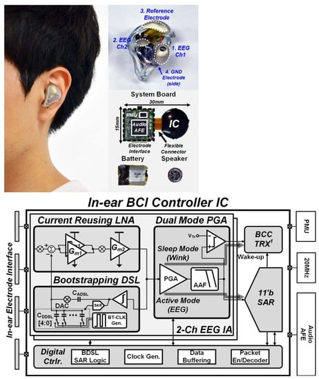
Figure 12.
Practical implementation of IC in the ear of a human (top). Presented IC structure in detail (bottom). Reprinted/adapted with permission from Ref. [25]: Copyright 2023, IEEE.
Liu et al. presented a wireless sensor–brain–machine interface (SBMI) system for joining the various sensors on the body of a human, restoring data through a tactile force sensor, an electro-goniometer, and fully integrated wireless BMI [24]. The main structure consists of an ADC, a receiver, and a transmitter, where the blocks of ultra-wideband (UWB) wireless transceivers [24] are shown.
A programmable electroencephalography monitoring system-on-a-chip (SoC) was presented in [16], where an ultra-low power TRX was implemented. The programmable SoC was generated using four sub-blocks, and a high-performance radio frequency TRX was one of the blocks. Figure 13 shows the general structure of the TRX, where the bias-stimulating circuit, a current-reuse self-mixing voltage control oscillator, a quadruple-transconductance power amplifier, and a matching circuit are used in the transmitter. In the receiver, a single-end input to differential-end output envelope detector, a level shifter, a baseband amplifier, and a hysteresis comparator are employed.

Figure 13.
Presented radio frequency TRX in [16].
In [35], a D-class amplifier was designed to improve the functionality. In this study, the architecture of a wireless power link that can be used for medical implants was presented. This PA was designed and simulated at the 180 nm CMOS technology, results in an efficiency greater than 80%, and operates up to 14 MHz with a 30 V supply voltage. The main part of this D-class PA consists of ML (i.e., n-type low-side DMOS transistor) and MH (p-type high-side DMOS transistor) [35].
To improve low-frequency noise performance, current-feedback instrumentation amplifier (CFIA) was presented in [49], which includes a switched capacitor (SC) integrator for providing a high-pass filter, resulting in offset reduction. This design was simulated in 130 nm CMOS technology with a 1 V supply voltage, 2.3 A current, and 125 dB CMRR specification. The general structure of the current feedback instrumentation amplifier is presented in Figure 14.
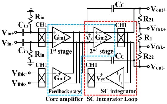
Figure 14.
Presented current feedback instrumentation amplifier in [49].
A general method for transferring power to medical implants is an inductive link that is driven by a Class-E PA. In [34], the simplified structure of an inductive link driven by a Class-E PA is depicted. One of the important schemes for data modulation is FSK, and the general structure of FSK data modulation is shown in Figure 15. This presented structure consists of a 7.1 H transmitter coil with a 1.2 H receiver coil. The actual measured PTE with power delivered to the load (PDL) specifications are 25% and 126 mW.
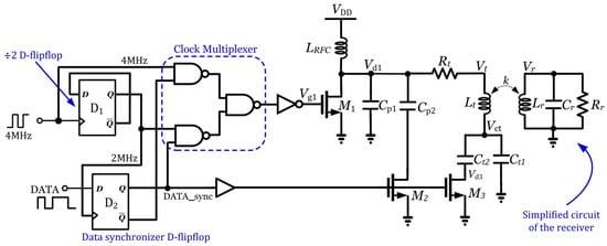
Figure 15.
Structure of the Class-E PA with FSK data modulation presented in [34]. Reprinted/adapted with permission: Copyright 2023, IEEE.
The block diagram of a neural recording system is presented in [50]. For this block, a suitable amplifier is designed that can be used for neural recording systems (see Figure 16). This amplifier is appropriate for bio-potential recording.
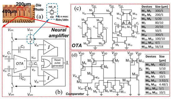
Figure 16.
Presented power system in [50] to be used in neural recording: (a) Rectangle presents the area where the amplifier is fabricated, (b) Just one type of comparator is required, (c) OTA design, (d) Comparator design. Reprinted/adapted with permission. Copyright 2023, IEEE.
The front-end amplifier (FEA) is another useful type of amplifier that can be used for detecting biosignals. For high-density implantable applications, an input impedance booster with current compensation feedback technique was presented in [51]. The presented amplifier was designed and simulated in 180 nm CMOS technology. The simulated results revealed an input impedance of 60 G and a CMRR of 61 dB. The operational transconductance amplifier (OTA) circuit is presented in Figure 17.
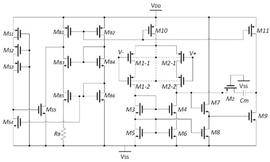
Figure 17.
Presented OTA design in [51].
Luo et al. presented a low total harmonic distortion (THD) chopper amplifier in [52] that is aimed at having a low level of noise. This amplifier was designed and simulated in 180 nm CMOS technology and has a power consumption of 3.24 W/channel, where the supply voltage is 1.8 V. The detailed structure of the very-low transconductance (VLT) OTA is presented in [52], and it results in suitable linearity.
Electrocardiogram (ECG) monitoring requires advanced wearable technologies that require sensors and integrated circuits. In [53], an on-chip integrated ECG signal acquisition system is presented where a OTA with a capacitive-resistive feedback network is employed. The signal-to-noise ratio differs from 35.7 dB to 38.6 dB. The experimental results reveal that the presented circuit can be used in long-term and wearable applications. The structure of the proposed design is provided in Figure 18.
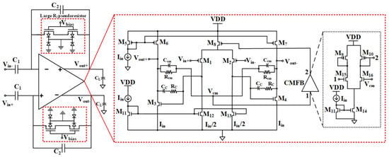
Figure 18.
Presented OTA design in [53]. Reprinted/adapted with permission: Copyright 2023, IEEE.
Song et al. presented a low-voltage current-reuse chopper-stabilized front-end amplifier that can be used for fetal ECG monitoring [54]. In this design, the peak charge-pump efficiency is 90%, and the consumed power is 1.56 W. The system’s concept is presented in Figure 19 with pop-outs to provide details.
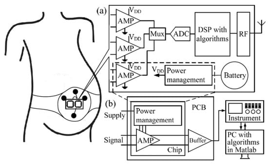
Figure 19.
Fetal ECG monitoring; (a) the overall system scheme, (b) close-up of the measurement setup [54]: Reprinted/adapted with permission: Copyright 2023, IEEE.
For concurrently monitoring EEG signals, in [55] a wearable active concentric electrode was presented, with body-coupled communication (BCC)-based concurrent recording/transmitting (see Figure 20). The presented system achieves 100 dB CMRR with a power consumption of 7.4 W.
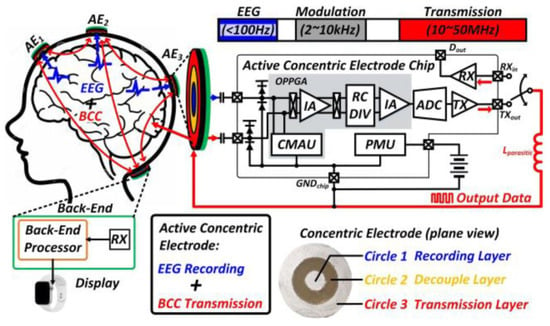
Figure 20.
The overall configuration of a wearable active concentric electrode [55]. Reprinted/adapted with permission: Copyright 2023, IEEE.
In [56], multi-channel biosignal recording systems were recorded to tackle the problems of CMRR reduction due to the impedance mismatch at the input terminals. For this case, an equivalent electrical circuit model of the input interface is provided in the study.
For medical ultrasonic transmitter applications, in [57] a high-voltage linear PA was designed, simulated, and measured. In this design, to reinforce the signal linearity of the amplifier, the digital predistortion (DPD) technique is applied, including a 7-bit digital-to-analog converter (DAC), an analog-to-digital converter, and a digital field-programmable gate array (FPGA). This amplifier achieves a power efficiency of 30%. The structure of PA includes low-voltage amplifier (LV AMP) and high-voltage current-feedback amplifier (HV CFA) is depicted in [57], where the linear amplifier is presented with the help of DPD.
Early detection of diseases can enable treatment to the highest degree. Hence, in [58], a compact electronic module for counting the biological living cells was presented. This design helps in sensing the unbalanced impedance between the sensing microelectrodes. The general measurement setup is provided in [58], which includes the instrumentation amplifier stage for sensing the difference in signals and also a lock-in amplifier stage for demodulating the signals.
In another study, a chopper-stabilized operational amplifier with low noise was presented [59]. The total current consumption is 117.2 A and the power supply is 1.8 V. A summary of the achieved results using this design is as follows: the DC gain is 132 dB, the CMRR is 192 dB, and the bandwidth is 2.69 MHz. The overall structure is presented in Figure 21.
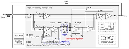
Figure 21.
Structure of chopper-stabilized operational amplifier presented in [59]. Reprinted/adapted with permission: Copyright 2023, IEEE.
For reducing the differential electrode offset, a low-power current feedback instrumentation amplifier is presented in [60]. The presented design is simulated in 180 nm CMOS technology, where the input noise is 3.8 V and the power consumption is 12.7 W.
In [61], optimization methods for designing wireless medical implant devices was presented. This method leads to optimized spiral coil designs for achieving maximum power transfer. For feeding the transmitter coil, a class-E amplifier was designed.
4. Biomedical Amplifiers from IC and Layout Perspectives
When designing amplifiers with CMOS technology, the layout is provided before fabrication, and the layout must pass LVS and DRC specifications in the simulation tool [62,63,64,65]. This section is devoted to the presentation of some examples of generated layouts for biomedical amplifiers.
In [66], based on indirect current feedback, a fully-differential (FD) instrumentation amplifier was designed with 180 nm CMOS technology, where the supply voltage was 1.8 V. The presented bandwidth was 5.83 MHz and the DC current consumption was 266.4 µA. Figure 22 shows the layout of IC with an area of 0.54 mm, and Figure 23 shows the proposed amplifier at the transistor level.
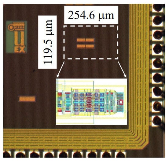
Figure 22.
Layout of presented amplifier in [66].

Figure 23.
Circuit design of generated layout in Figure 22 where the design is captured from [66].
The integrated amplifier presented in [67] includes operational transconductance amplifier, chopper input, folded cascode, inverter-based input, multistage amplifier, and current reuse, and the general layout is presented in Figure 24.
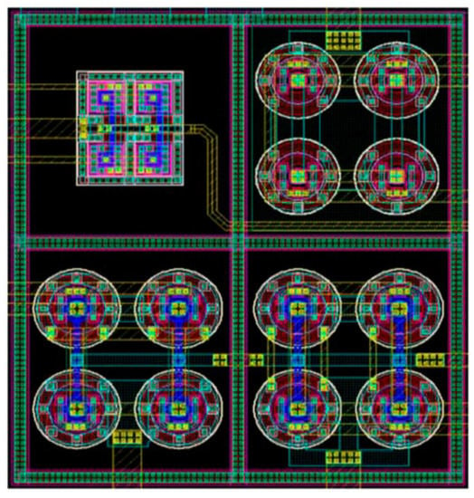
Figure 24.
Layout of amplifier IC presented in [67].
5. Biomedical Applications from the Measurement Perspective
For any of the designs presented above, providing a suitable measurement setup is also an essential task. This section is devoted to the presentation of various aspects of medical measurements such as an integrated analog readout for multi-frequency bioimpedance measurements, an AC instrumentation amplifier for bioimpedance measurements, and an analog realization of a fractional-order skin-electrode model for tetrapolar bioimpedance measurements.
For the measurement aspect, Cheon et al. presented an effective impedance measurement feature for bioimpedance consideration, where it measures the magnitude and the real part of the complex impedance [68]. Figure 25 shows the presented electrochemical impedance spectroscopy system, which measures the impedance over the targeted frequency band. The consumed power is 513 µW, and the accuracy of measurement is improved by 30% in comparison to the conventional measurement methods.

Figure 25.
General structure of electrochemical impedance spectroscopy presented in [68] with a combination of voltage-controlled current source (VCCS), integrated circuit (IC), and instrumentation amplifier (IA).
In another study, an indirect current feedback method was presented for conducting bioimpedance measurements [69]. It uses degeneration resistors where the resistors are low. The design was simulated in 180 nm CMOS technology where the voltage gain is 4 v/v with 1.8 V supply voltage. The general structure of the presented indirect current feedback method is illustrated in Figure 26.
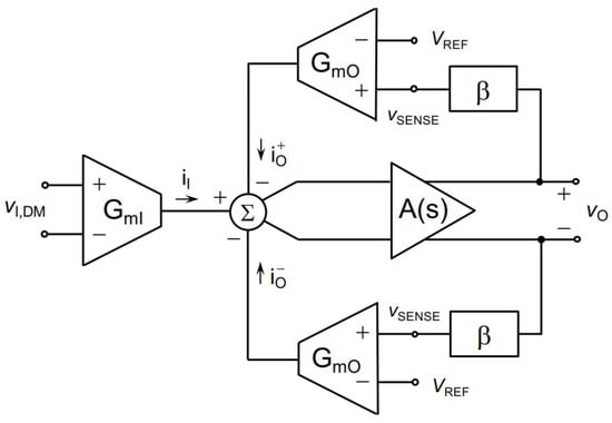
Figure 26.
General structure of indirect current feedback presented in [69].
Another method for bioimpedance measurements was described in [70] and was simulated in 90 nm CMOS technology. The presented method is based on the fractional-order capacitor emulator that is shown in Figure 27. The simulation results demonstrated that the magnitude is low and the phase error is minimal; hence, the presented structure is suitable for bioimpedance measuring situations of up to 10 KHz.
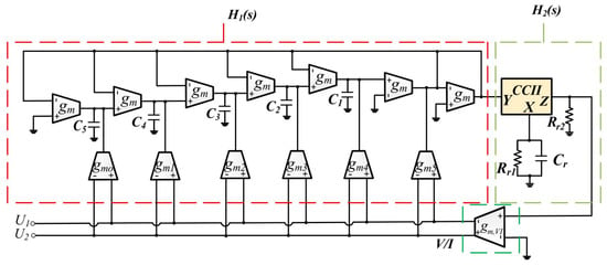
Figure 27.
The general design of fractional-order capacitor emulator presented in [70].
Table 1, at the end of this section summarizes the various contributions and specifications of each reported work in this study.

Table 1.
Summary of some reported biomedical amplifiers with the focuses and output specifications of each one.
6. Conclusions
In healthcare communication systems, providing high-performance biomedical devices is critical, as the recognition of any disease and its treatment depends greatly on the performance of these devices. Typically, the effectiveness of each medical device depends on the application of each one. Amplifiers are the most important part of medical devices, especially for the implanted devices. They are employed for various applications with vastly different topologies and structures. This survey is devoted to the summary of the designed amplifiers in very recently published literature aimed at usage in medical applications. By reading this review, researchers can obtain a general view of the various amplifier designs and can find a suitable design for their problems. In the future, the importance of emerging fifth-generation (5G) and next-generation technologies can be studied in biomedical amplifiers, because these technologies provide a platform for transferring data between the patient and medical doctors.
Author Contributions
Conceptualization, L.K. and I.P.; methodology, L.M.; investigation, L.K. and L.M.; resources, I.P. and L.M.; data curation, L.K.; writing—original draft preparation, L.K.; writing—review and editing, L.M. and I.P.; visualization, L.K.; supervision, L.M.; project administration, I.P.; funding acquisition, I.P. All authors have read and agreed to the published version of the manuscript.
Funding
This work was partially supported by a grant of the Romanian Ministry of Education and Research, CNCS-UEFISCDI, project number PN-III-P4-ID-PCE-2020-0404, within PNCDI III.
Institutional Review Board Statement
Not applicable.
Informed Consent Statement
Not applicable.
Data Availability Statement
Not applicable.
Conflicts of Interest
The authors declare no conflict of interest.
References
- Singh, W.; Deb, S.; Bahubalindruni, P. Low-Noise Energy Efficient Readout Front-End for Wearable Continuous Blood Pressure Monitoring Systems. IEEE Trans. Consum. Electron. 2020, 66, 318–326. [Google Scholar] [CrossRef]
- Neihart, N.; Harrison, R. Micropower circuits for bidirectional wireless telemetry in neural recording applications. IEEE Trans. Biomed. Eng. 2005, 52, 1950–1959. [Google Scholar] [CrossRef] [PubMed]
- Liu, C.; Yang, X.M.; Guo, Y.X.; Liu, X. Design of an integrated on-chip implantable antenna for a neuromicrosystem. In Proceedings of the 2016 IEEE MTT-S International Microwave Workshop Series on Advanced Materials and Processes for RF and THz Applications (IMWS-AMP), Chengdu, China, 20–22 July 2016; pp. 1–3. [Google Scholar] [CrossRef]
- Yakovlev, A.; Kim, S.; Poon, A. Implantable biomedical devices: Wireless powering and communication. IEEE Commun. Mag. 2012, 50, 152–159. [Google Scholar] [CrossRef]
- Xia, Y.; Fan, Y. Security Analysis of Sports Injury Medical System Based on Internet of Health Things Technology. IEEE Access 2020, 8, 211358–211370. [Google Scholar] [CrossRef]
- Chiu, C.Y.; Zhang, Z.C.; Lin, T.H. Design of a 0.6-V, 429-MHz FSK Transceiver Using Q-Enhanced and Direct Power Transfer Techniques in 90-nm CMOS. IEEE J. Solid-State Circuits 2020, 55, 3024–3035. [Google Scholar] [CrossRef]
- Zhang, F.; Miyahara, Y.; Otis, B.P. Design of a 300-mV 2.4-GHz Receiver Using Transformer-Coupled Techniques. IEEE J. Solid-State Circuits 2013, 48, 3190–3205. [Google Scholar] [CrossRef]
- Jiang, D.; Wu, Y.; Demosthenous, A. Hand Gesture Recognition Using Three-Dimensional Electrical Impedance Tomography. IEEE Trans. Circuits Syst. II Express Briefs 2020, 67, 1554–1558. [Google Scholar] [CrossRef]
- Surakitbovorn, K.; Rivas-Davila, J.M. Modular ON/OFF and Phase-Shifting for High-Speed Radio Frequency Power Modulation. IEEE Open J. Power Electron. 2020, 1, 393–406. [Google Scholar] [CrossRef]
- Pavelić, L.; Lacković, I.; Mihić, M.S.; Prlić, I. SiPM-Based Detector for High-Resolution Measurements in Pulsed Radiation Fields. IEEE Trans. Instrum. Meas. 2021, 70, 1–8. [Google Scholar] [CrossRef]
- Byzova, A.; Hekmatmanesh, A.; Roozbahani, H.; Handroos, H.; Hakansson, N.; Lankarani, H.M. Real-Time Human Body and Brain Monitoring During Horseback Riding Simulator by Means of Inertial Motion Capture and EEG Systems. IEEE Access 2020, 8, 162163–162171. [Google Scholar] [CrossRef]
- Ratametha, C.; Tepwimonpetkun, S.; Wattanapanitch, W. A 2.64-μW 71-dB SNDR Discrete-Time Signal-Folding Amplifier for Reducing ADC’s Resolution Requirement in Wearable ECG Acquisition Systems. IEEE Trans. Biomed. Circuits Syst. 2020, 14, 48–64. [Google Scholar] [CrossRef]
- Song, H.S.; Lee, S.H.; Ghergherehchi, M.; Kim, H.S.; Lee, J.C.; Oh, S.Y.; Hur, M.G.; Chai, J.S. Modular 20 kW, 83.2-MHz Solid-State RF Amplifier for a 10-MeV Cyclotron. IEEE Trans. Nucl. Sci. 2019, 66, 1924–1930. [Google Scholar] [CrossRef]
- Al-Atawi, A.A.; Khan, F.; Kim, C.G. Application and Challenges of IoT Healthcare System in COVID-19. Sensors 2022, 22, 7304. [Google Scholar] [CrossRef] [PubMed]
- Miglani, R.; Malhotra, J.S.; Majumdar, A.K.; Tubbal, F.; Raad, R. Multi-Hop Relay Based Free Space Optical Communication Link for Delivering Medical Services in Remote Areas. IEEE Photonics J. 2020, 12, 1–21. [Google Scholar] [CrossRef]
- Lee, S.Y.; Tsou, C.; Liao, Z.X.; Cheng, P.H.; Huang, P.W.; Lee, H.Y.; Lin, C.C.; Shieh, G.S. A Programmable EEG Monitoring SoC With Optical and Electrical Stimulation for Epilepsy Control. IEEE Access 2020, 8, 92196–92211. [Google Scholar] [CrossRef]
- Koo, N.; Cho, S. A 24.8-μW Biopotential Amplifier Tolerant to 15-VPP Common-Mode Interference for Two-Electrode ECG Recording in 180 nm CMOS. IEEE J. Solid-State Circuits 2021, 56, 591–600. [Google Scholar] [CrossRef]
- Cochran, Z.; Ytterdal, T.; Madan, A.; Rizkalla, M. High Speed Terahertz Devices via Emerging Hybrid GNRFET/Josephson Junction Technologies. IEEE Trans. Appl. Supercond. 2020, 30, 1–11. [Google Scholar] [CrossRef]
- Kim, J.; Ko, H. Self-Biased Ultralow Power Current-Reused Neural Amplifier with on-Chip Analog Spike Detections. IEEE Access 2019, 7, 109792–109803. [Google Scholar] [CrossRef]
- Different Parts of Body Suitable for Implanted Devices. Available online: http://technologyandsociety.org/implantable-technology/ (accessed on 25 January 2022).
- Karimi-Bidhendi, A.; Malekzadeh-Arasteh, O.; Lee, M.C.; McCrimmon, C.M.; Wang, P.T.; Mahajan, A.; Liu, C.Y.; Nenadic, Z.; Do, A.H.; Heydari, P. CMOS Ultralow Power Brain Signal Acquisition Front-Ends: Design and Human Testing. IEEE Trans. Biomed. Circuits Syst. 2017, 11, 1111–1122. [Google Scholar] [CrossRef]
- Hannan, M.A.; Hussein, H.A.; Mutashar, S.; Samad, S.A.; Hussain, A. Automatic Frequency Controller for Power Amplifiers Used in Bio-Implanted Applications: Issues and Challenges. Sensors 2014, 14, 23843. [Google Scholar] [CrossRef]
- Kouhalvandi, L.; Matekovits, L.; Peter, I. Magic of 5G Technology and Optimization Methods Applied to Biomedical Devices: A Survey. Appl. Sci. 2022, 12, 7096. [Google Scholar] [CrossRef]
- Liu, X.; Zhu, H.; Zhang, M.; Wu, X.; Richardson, A.G.; Sritharan, S.Y.; Ge, D.; Shu, Y.; Lucas, T.H.; Van der Spiegel, J. A fully integrated wireless sensor-brain interface system to restore finger sensation. In Proceedings of the 2017 IEEE International Symposium on Circuits and Systems (ISCAS), Baltimore, MD, USA, 28–31 May 2017; pp. 1–4. [Google Scholar] [CrossRef]
- Lee, J.; Lee, K.R.; Ha, U.; Kim, J.H.; Lee, K.; Gweon, S.; Jang, J.; Yoo, H.J. A 0.8-V 82.9-μW In-Ear BCI Controller IC With 8.8 PEF EEG Instrumentation Amplifier and Wireless BAN Transceiver. IEEE J. Solid-State Circuits 2019, 54, 1185–1195. [Google Scholar] [CrossRef]
- Stanslaski, S.; Herron, J.; Chouinard, T.; Bourget, D.; Isaacson, B.; Kremen, V.; Opri, E.; Drew, W.; Brinkmann, B.H.; Gunduz, A.; et al. A Chronically Implantable Neural Coprocessor for Investigating the Treatment of Neurological Disorders. IEEE Trans. Biomed. Circuits Syst. 2018, 12, 1230–1245. [Google Scholar] [CrossRef]
- Huang, J.; Laiwalla, F.; Lee, J.; Cui, L.; Leung, V.; Nurmikko, A.; Mercier, P.P. A 0.01-mm2 Mostly Digital Capacitor-Less AFE for Distributed Autonomous Neural Sensor Nodes. IEEE Solid-State Circuits Lett. 2018, 1, 162–165. [Google Scholar] [CrossRef]
- Lyu, L.; Ye, D.; Shi, C.J.R. A 340 nW/Channel 110 dB PSRR Neural Recording Analog Front-End Using Replica-Biasing LNA, Level-Shifter Assisted PGA, and Averaged LFP Servo Loop in 65 nm CMOS. IEEE Trans. Biomed. Circuits Syst. 2020, 14, 811–824. [Google Scholar] [CrossRef]
- Lin, Y.P.; Yeh, C.Y.; Huang, P.Y.; Wang, Z.Y.; Cheng, H.H.; Li, Y.T.; Chuang, C.F.; Huang, P.C.; Tang, K.T.; Ma, H.P.; et al. A Battery-Less, Implantable Neuro-Electronic Interface for Studying the Mechanisms of Deep Brain Stimulation in Rat Models. IEEE Trans. Biomed. Circuits Syst. 2016, 10, 98–112. [Google Scholar] [CrossRef]
- Cruz, H.; Huang, H.Y.; Lee, S.Y.; Luo, C.H. A 1.3 mW low-IF, current-reuse, and current-bleeding RF front-end for the MICS band with sensitivity of -97 dbm. IEEE Trans. Circuits Syst. I Regul. Pap. 2015, 62, 1627–1636. [Google Scholar] [CrossRef]
- Zamani, M.; Rezaeiyan, Y.; Huynh, H.A.; Ronchini, M.; Farkhani, H.; Moradi, F. A 2.3-μW Capacitively Coupled Chopper-Stabilized Neural Amplifier With Input Impedance of 6.7 GΩ. IEEE Solid-State Circuits Lett. 2021, 4, 133–136. [Google Scholar] [CrossRef]
- Lee, S.Y.; Cheng, P.H.; Tsou, C.F.; Lin, C.C.; Shieh, G.S. A 2.4 GHz ISM Band OOK Transceiver With High Energy Efficiency for Biomedical Implantable Applications. IEEE Trans. Biomed. Circuits Syst. 2020, 14, 113–124. [Google Scholar] [CrossRef]
- Ghanad, M.A.; Green, M.M.; Dehollain, C. A 30 μW Remotely Powered Local Temperature Monitoring Implantable System. IEEE Trans. Biomed. Circuits Syst. 2017, 11, 54–63. [Google Scholar] [CrossRef]
- Ahmadi, M.M.; Ghandi, S. A Class-E Power Amplifier With Wideband FSK Modulation for Inductive Power and Data Transmission to Medical Implants. IEEE Sens. J. 2018, 18, 7242–7252. [Google Scholar] [CrossRef]
- Valente, V.; Eder, C.; Donaldson, N.; Demosthenous, A. A High-Power CMOS Class-D Amplifier for Inductive-Link Medical Transmitters. IEEE Trans. Power Electron. 2015, 30, 4477–4488. [Google Scholar] [CrossRef]
- Wang, S.; Garakoui, S.K.; Chun, H.; Salinas, D.G.; Sijbers, W.; Putzeys, J.; Martens, E.; Craninckx, J.; Van Helleputte, N.; Lopez, C.M. A Compact Quad-Shank CMOS Neural Probe with 5120 Addressable Recording Sites and 384 Fully Differential Parallel Channels. IEEE Trans. Biomed. Circuits Syst. 2019, 13, 1625–1634. [Google Scholar] [CrossRef]
- Hansen, S.; Bredendiek, C.; Briese, G.; Pohl, N. A Compact Harmonic Radar System With Active Tags at 61/122 GHz ISM Band in SiGe BiCMOS for Precise Localization. IEEE Trans. Microw. Theory Tech. 2021, 69, 906–915. [Google Scholar] [CrossRef]
- Laurila, M.M.; Matsui, H.; Shiwaku, R.; Peltokangas, M.; Verho, J.; Montero, K.L.; Sekine, T.; Vehkaoja, A.; Oksala, N.; Tokito, S.; et al. A Fully Printed Ultra-Thin Charge Amplifier for On-Skin Biosignal Measurements. IEEE J. Electron Devices Soc. 2019, 7, 566–574. [Google Scholar] [CrossRef]
- Mirbozorgi, S.A.; Bahrami, H.; Sawan, M.; Rusch, L.A.; Gosselin, B. A Single-Chip Full-Duplex High Speed Transceiver for Multi-Site Stimulating and Recording Neural Implants. IEEE Trans. Biomed. Circuits Syst. 2016, 10, 643–653. [Google Scholar] [CrossRef]
- Jia, Y.; Guler, U.; Lai, Y.P.; Gong, Y.; Weber, A.; Li, W.; Ghovanloo, M. A Trimodal Wireless Implantable Neural Interface System-on-Chip. IEEE Trans. Biomed. Circuits Syst. 2020, 14, 1207–1217. [Google Scholar] [CrossRef]
- Ng, K.A.; Yuan, C.; Rusly, A.; Do, A.T.; Zhao, B.; Liu, S.C.; Peh, W.Y.X.; Thow, X.Y.; Voges, K.; Lee, S.; et al. A Wireless Multi-Channel Peripheral Nerve Signal Acquisition System-on-Chip. IEEE J. Solid-State Circuits 2019, 54, 2266–2280. [Google Scholar] [CrossRef]
- Sutardja, C.; Rabaey, J.M. Isolator-Less Near-Field RFID Reader for Sub-Cranial Powering/Data Link of Millimeter-Sized Implants. IEEE J. Solid-State Circuits 2018, 53, 2032–2042. [Google Scholar] [CrossRef]
- Lin, J.Y.; Chen, H.C.; Yen, M.Y. Sensor/Antenna Interface IC for Implantable Biomedical Monitoring System. IEEE Trans. Microw. Theory Tech. 2018, 66, 1660–1667. [Google Scholar] [CrossRef]
- Copani, T.; Min, S.; Shashidharan, S.; Chakraborty, S.; Stevens, M.; Kiaei, S.; Bakkaloglu, B. A CMOS Low-Power Transceiver With Reconfigurable Antenna Interface for Medical Implant Applications. IEEE Trans. Microw. Theory Tech. 2011, 59, 1369–1378. [Google Scholar] [CrossRef]
- Yang, C.L.; Tsai, C.L.; Cheng, K.T.; Chen, S.H. Low-Invasive Implantable Devices of Low-Power Consumption Using High-Efficiency Antennas for Cloud Health Care. IEEE J. Emerg. Sel. Top. Circuits Syst. 2012, 2, 14–23. [Google Scholar] [CrossRef]
- Abdulmalek, S.; Nasir, A.; Jabbar, W.A.; Almuhaya, M.A.M.; Bairagi, A.K.; Khan, M.A.M.; Kee, S.H. IoT-Based Healthcare-Monitoring System towards Improving Quality of Life: A Review. Healthcare 2022, 10, 1993. [Google Scholar] [CrossRef]
- Park, B.; Kwon, K. 2.4-GHz Bluetooth Low Energy Receiver Employing New Quadrature Low-Noise Amplifier for Low-Power Low-Voltage IoT Applications. IEEE Trans. Microw. Theory Tech. 2021, 69, 1887–1895. [Google Scholar] [CrossRef]
- Han, Z.; Xu, J.; Yang, C.; Wang, N.; Li, Z.; Cui, Y.; Jian, X. A High Sensitivity 20-MHz Endoscopic Transducer With Integrated Miniature Amplifier. IEEE Access 2020, 8, 109241–109248. [Google Scholar] [CrossRef]
- Lee, C.J.; Song, J.I. A Chopper Stabilized Current-Feedback Instrumentation Amplifier for EEG Acquisition Applications. IEEE Access 2019, 7, 11565–11569. [Google Scholar] [CrossRef]
- Chen, Y.; Basu, A.; Liu, L.; Zou, X.; Rajkumar, R.; Dawe, G.S.; Je, M. A Digitally Assisted, Signal Folding Neural Recording Amplifier. IEEE Trans. Biomed. Circuits Syst. 2014, 8, 528–542. [Google Scholar] [CrossRef]
- Zhou, Z. A Front-End Amplifier With Current Compensation Feedback Input Impedance Booster for Neural Signal Applications. IEEE Access 2020, 8, 178055–178062. [Google Scholar] [CrossRef]
- Luo, D.; Zhang, M.; Wang, Z. A Low-Noise Chopper Amplifier Designed for Multi-Channel Neural Signal Acquisition. IEEE J. Solid-State Circuits 2019, 54, 2255–2265. [Google Scholar] [CrossRef]
- Tasneem, N.T.; Pullano, S.A.; Critello, C.D.; Fiorillo, A.S.; Mahbub, I. A Low-Power On-Chip ECG Monitoring System Based on MWCNT/PDMS Dry Electrodes. IEEE Sens. J. 2020, 20, 12799–12806. [Google Scholar] [CrossRef]
- Song, S.; Rooijakkers, M.; Harpe, P.; Rabotti, C.; Mischi, M.; van Roermund, A.H.M.; Cantatore, E. A Low-Voltage Chopper-Stabilized Amplifier for Fetal ECG Monitoring With a 1.41 Power Efficiency Factor. IEEE Trans. Biomed. Circuits Syst. 2015, 9, 237–247. [Google Scholar] [CrossRef]
- Tang, T.; Yan, L.; Park, J.H.; Wu, H.; Zhang, L.; Li, J.; Dong, Y.; Lee, B.H.Y.; Yoo, J. An Active Concentric Electrode for Concurrent EEG Recording and Body-Coupled Communication (BCC) Data Transmission. IEEE Trans. Biomed. Circuits Syst. 2020, 14, 1253–1262. [Google Scholar] [CrossRef]
- Malekzadeh-Arasteh, O.; Danesh, A.R.; Do, A.H.; Nenadic, Z.; Heydari, P. An Analysis of CMRR Degradation in Multi-Channel Biosignal Recording Systems. IEEE Trans. Circuits Syst. II Express Briefs 2021, 68, 151–155. [Google Scholar] [CrossRef]
- Gao, Z.; Gui, P.; Jordanger, R. An Integrated High-Voltage Low-Distortion Current-Feedback Linear Power Amplifier for Ultrasound Transmitters Using Digital Predistortion and Dynamic Current Biasing Techniques. IEEE Trans. Circuits Syst. II Express Briefs 2014, 61, 373–377. [Google Scholar] [CrossRef]
- Quang, L.D.; Bui, T.T.; Hoang, B.A.; Nhu, C.N.; Thuy, H.T.T.; Jen, C.P.; Duc, T.C. Biological Living Cell in-Flow Detection Based on Microfluidic Chip and Compact Signal Processing Circuit. IEEE Trans. Biomed. Circuits Syst. 2020, 14, 1371–1380. [Google Scholar] [CrossRef] [PubMed]
- Kim, H.; Han, K.; Kim, J.; You, D.; Heo, H.; Kwon, Y.; Kim, C.Y.; Lee, H.D.; Ko, H. Chopper-Stabilized Low-Noise Multipath Operational Amplifier With Dual Ripple Rejection Loops. IEEE Trans. Circuits Syst. II Express Briefs 2020, 67, 2427–2431. [Google Scholar] [CrossRef]
- Hoseini, Z.; Nazari, M.; Lee, K.S.; Chung, H. Current Feedback Instrumentation Amplifier With Built-In Differential Electrode Offset Cancellation Loop for ECG/EEG Sensing Frontend. IEEE Trans. Instrum. Meas. 2021, 70, 1–11. [Google Scholar] [CrossRef]
- Nguyen, M.Q.; Hughes, Z.; Woods, P.; Seo, Y.S.; Rao, S.; Chiao, J.C. Field Distribution Models of Spiral Coil for Misalignment Analysis in Wireless Power Transfer Systems. IEEE Trans. Microw. Theory Tech. 2014, 62, 920–930. [Google Scholar] [CrossRef]
- Kim, H.R.; An, C.H.; Kong, B.S. High-Speed Column Driver IC Having Buffer Amplifier with Embedded Isolation Switch and Compact Adaptive Biasing for Flat-Panel Displays. Electronics 2021, 10, 2309. [Google Scholar] [CrossRef]
- Sajedin, M.; Elfergani, I.; Rodriguez, J.; Abd-Alhameed, R.; Fernandez-Barciela, M.; Violas, M. Ultra-Compact mm-Wave Monolithic IC Doherty Power Amplifier for Mobile Handsets. Electronics 2021, 10, 2131. [Google Scholar] [CrossRef]
- Alonso Rivas, E.; Scandurra, G.; Ciofi, C.; Rodríguez-Morcillo García, C.; Giannetti, R. A Novel Approach for the Design of Fast-Settling Amplifiers for Biosignal Detection. Electronics 2021, 10, 2631. [Google Scholar] [CrossRef]
- Jaikla, W.; Buakhong, U.; Siripongdee, S.; Khateb, F.; Sotner, R.; Silapan, P.; Suwanjan, P.; Chaichana, A. Single Commercially Available IC-Based Electronically Controllable Voltage-Mode First-Order Multifunction Filter with Complete Standard Functions and Low Output Impedance. Sensors 2021, 21, 7376. [Google Scholar] [CrossRef] [PubMed]
- Corbacho, I.; Carrillo, J.M.; Ausín, J.L.; Domínguez, M.Á.; Pérez-Aloe, R.; Duque-Carrillo, J.F. A Fully-Differential CMOS Instrumentation Amplifier for Bioimpedance-Based IoT Medical Devices. J. Low Power Electron. Appl. 2023, 13, 3. [Google Scholar] [CrossRef]
- Simmich, S.; Bahr, A.; Rieger, R. Noise Efficient Integrated Amplifier Designs for Biomedical Applications. Electronics 2021, 10, 1522. [Google Scholar] [CrossRef]
- Cheon, S.I.; Kweon, S.J.; Kim, Y.; Koo, J.; Ha, S.; Je, M. An Impedance Readout IC with Ratio-Based Measurement Techniques for Electrical Impedance Spectroscopy. Sensors 2022, 22, 1563. [Google Scholar] [CrossRef]
- Corbacho, I.; Carrillo, J.M.; Ausín, J.L.; Domínguez, M.Á.; Pérez-Aloe, R.; Duque-Carrillo, J.F. Compact CMOS Wideband Instrumentation Amplifiers for Multi-Frequency Bioimpedance Measurement: A Design Procedure. Electronics 2022, 11, 1668. [Google Scholar] [CrossRef]
- Alimisis, V.; Dimas, C.; Pappas, G.; Sotiriadis, P.P. Analog Realization of Fractional-Order Skin-Electrode Model for Tetrapolar Bio-Impedance Measurements. Technologies 2020, 8, 61. [Google Scholar] [CrossRef]
Disclaimer/Publisher’s Note: The statements, opinions and data contained in all publications are solely those of the individual author(s) and contributor(s) and not of MDPI and/or the editor(s). MDPI and/or the editor(s) disclaim responsibility for any injury to people or property resulting from any ideas, methods, instructions or products referred to in the content. |
© 2023 by the authors. Licensee MDPI, Basel, Switzerland. This article is an open access article distributed under the terms and conditions of the Creative Commons Attribution (CC BY) license (https://creativecommons.org/licenses/by/4.0/).
